Group Assignment:
- Use the test equipment in your lab to observe the operation of a microcontroller circuit board (as a minimum, you should demonstrate the use of a multimeter and oscilloscope)
- Document your work on the group work page and reflect what you learned on your individual page
Individual Assignment:
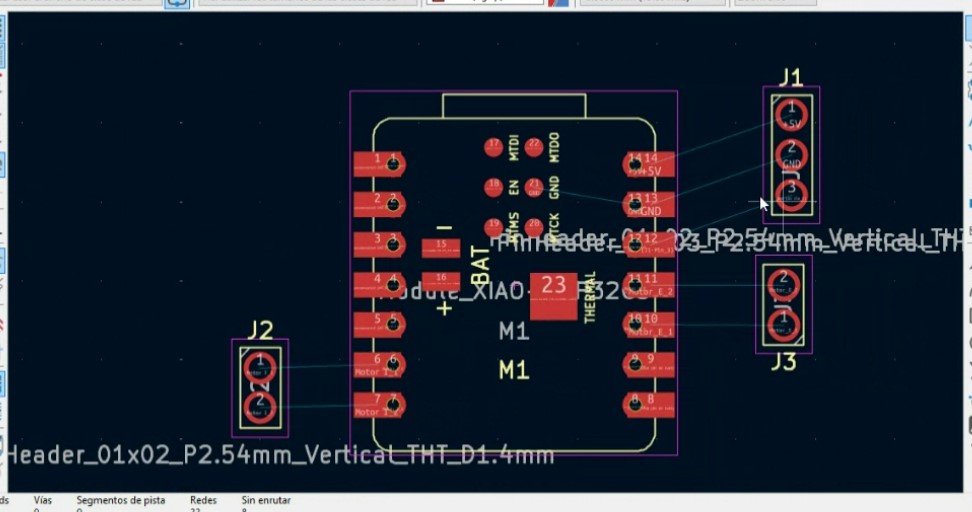
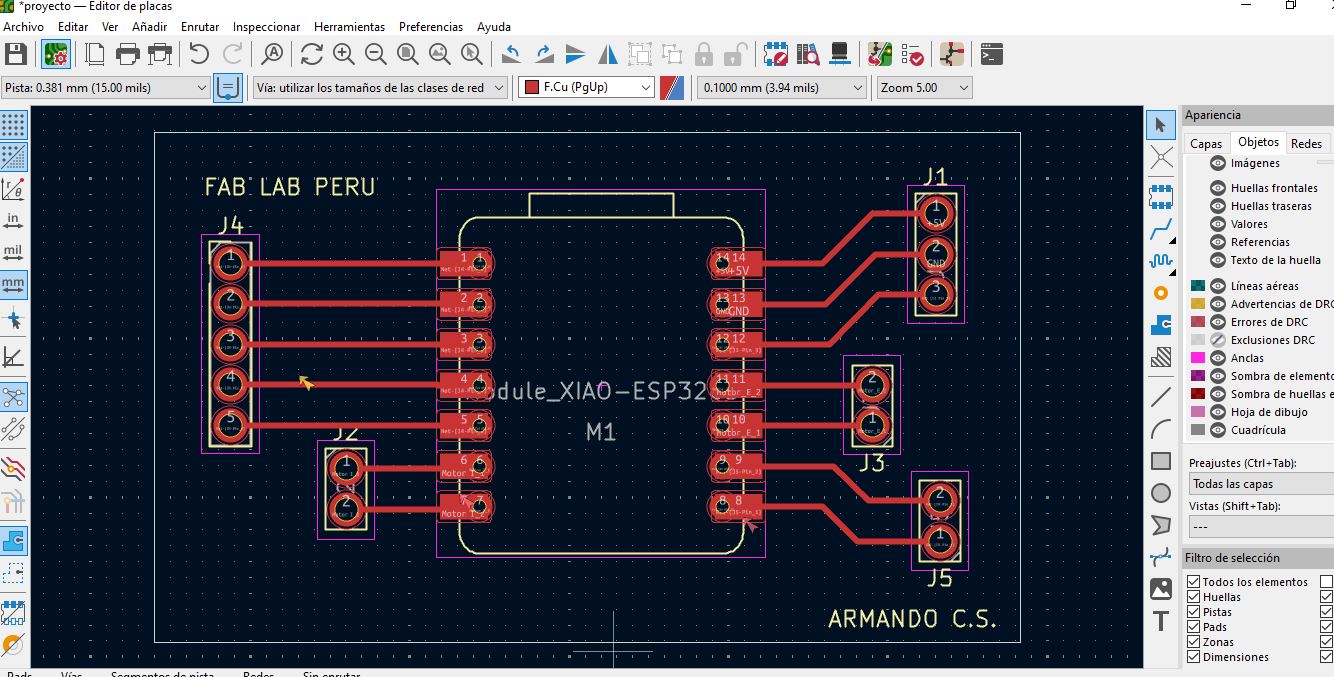
- Use an EDA tool to design a development board that uses parts from the inventory to interact and communicate with an embedded microcontroller.
- extra credit: try another design workflow
- extra credit: simulate your design
- extra credit: design a case around your design
Have you answered these questions?
- Linked to the group assignment page. ✅
- Documented what you have learned in electronics design. ✅
- Checked your board can be fabricated. ✅
- Explained problems and how you fixed them. ✅
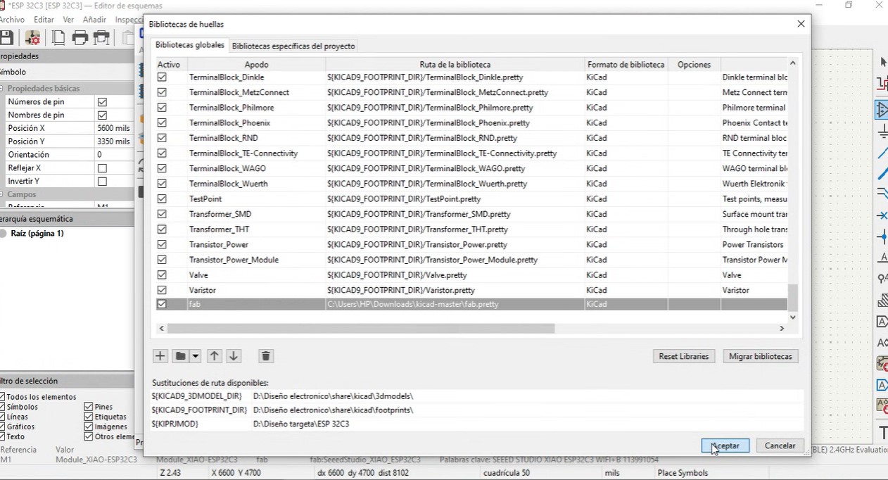
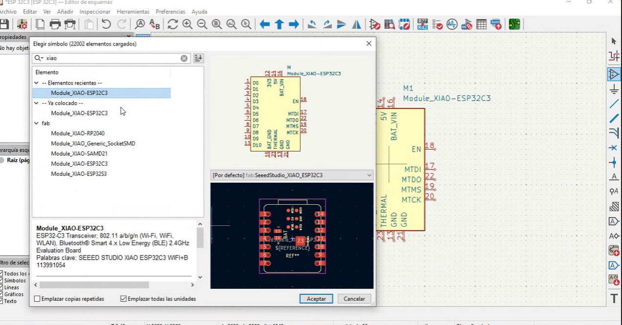
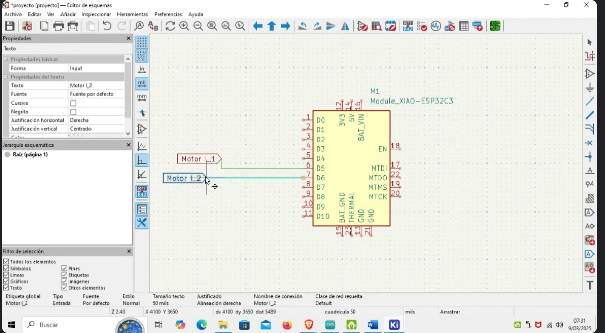
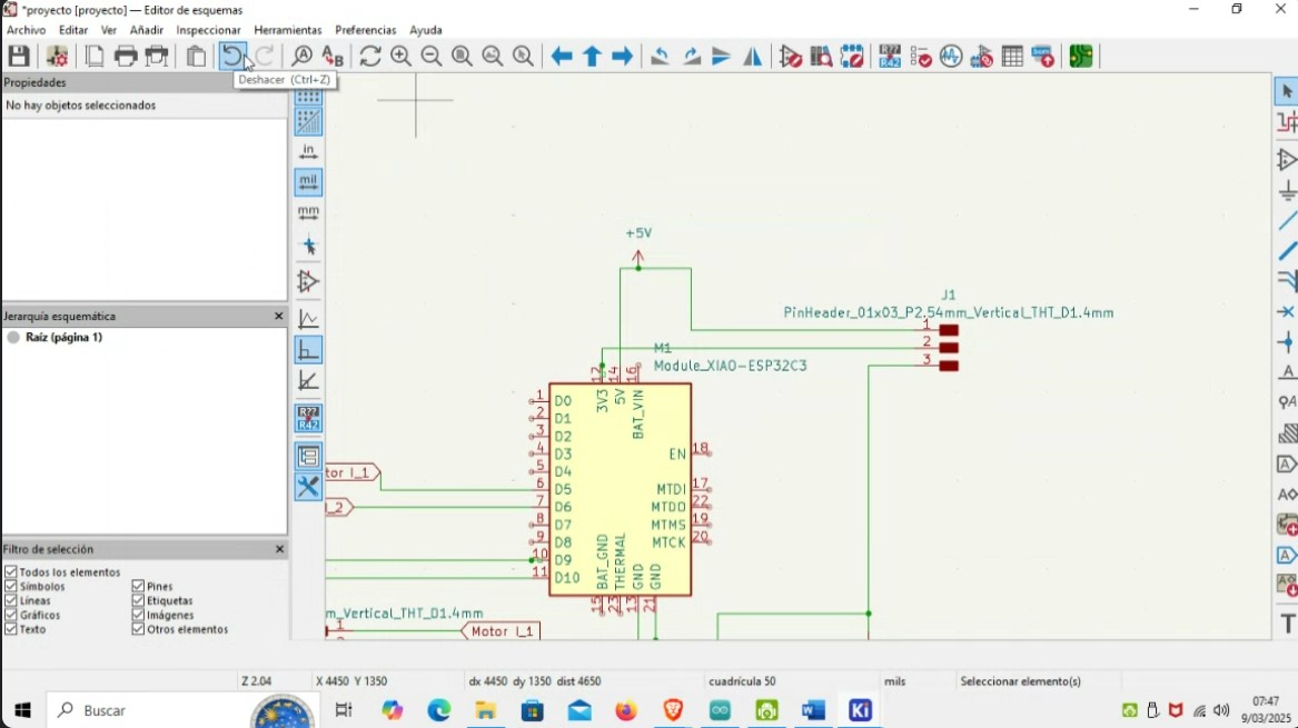
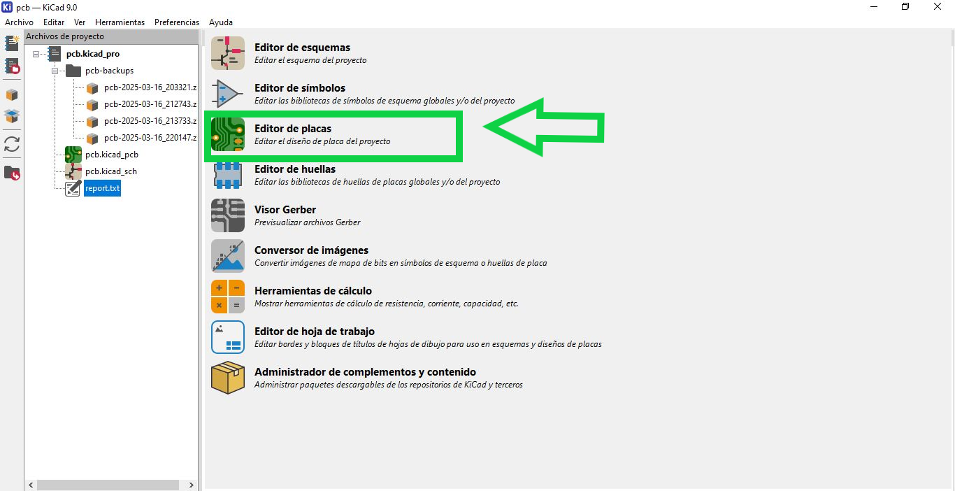
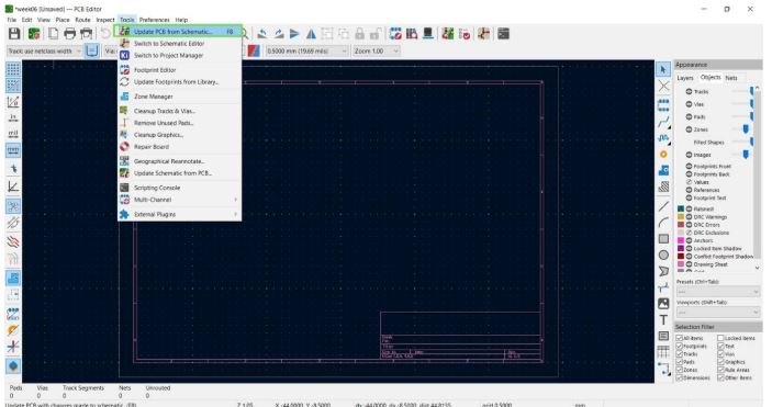
- Included original design files (Eagle, KiCad, etc.) ✅
- Included a ‘hero shot’ ✅
Group Assignment
- Use the test equipment in your lab to observe the operation of a microcontroller circuit board (as a minimum, you should demonstrate the use of a multimeter and oscilloscope)
- Document your work on the group work page and reflect what you learned on your individual page
Teamwork
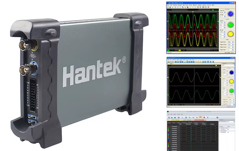
For this task, I used my personal oscilloscope, since the UNCP Fab Lab where I work doesn't currently have this testing instrument. So, I made the most of this instrument, as it's a PC oscilloscope with a good bandwidth (20 MHz). The software is intuitive.
In addition, it allowed me to better understand the concepts of measuring different signals. This measuring instrument is very similar to a bench oscilloscope.
The oscilloscope I worked with is the Hantek 6022BE, a 2-channel digital oscilloscope that connects via USB to a PC or laptop. Below are its technical specifications.
On the other hand, for electrical measurements, use the Mestek DM90E multimeter, a compact and portable digital multimeter, a reliable and versatile tool for those who need to take accurate electrical measurements in a variety of environments. Its combination of advanced features and affordable price makes it an attractive option for professionals and amateurs alike; it is a versatile and accurate tool for electrical measurements. Its main features are detailed below:
Hantek 6022BE Digital Oscilloscope
📊 Technical Specifications
- Channels: 2 analog
- Bandwidth: 20 MHz
- Sampling rate: Up to 48 MSa/s
- Vertical resolution: 8 bits
- Input impedance: 1 MΩ // 25 pF
- Input sensitivity: 20 mV/div to 5 V/div
- DC accuracy: ±3%
- Time base range: 1 ns/div to 5 ks/div
- Memory depth: Up to 1 Mpts
- Input coupling: AC/DC/GND
- Input protection: Diode clamping
- Interface: USB 2.0
Mestek DM90E Digital Multimeter
📊 Technical Specifications
- DC Voltage: 600 mV / 6 V / 60 V / 600 V
- AC Voltage: 6 V / 60 V / 600 V
- DC Current: 60 mA / 600 mA / 10 A
- AC Current: 60 mA / 600 mA / 10 A
- Resistance: 600 Ω / 6 kΩ / 60 kΩ / 600 kΩ / 6 MΩ / 60 MΩ
- Capacitance: 60 nF / 600 nF / 6 µF / 60 µF / 600 µF / 6 mF / 100 mF
- Frequency: 60 Hz / 600 Hz / 6 kHz / 60 kHz / 600 kHz / 10 MHz
- Temperature Range: -20°C to 1000°C (with K-type thermocouple)
- Non-contact Voltage Detection (NCV): 90 ~ 1000 V AC
- Display: 1999-count LCD with backlight
- Sampling Rate: 3 times per second
- Power Supply: 3 x AAA 1.5 V batteries
Reflections
- While performing the measurements, I understood several fundamental concepts, since measurements with an oscilloscope and multimeter are essential in electronics, electricity, and engineering because they allow us to verify, diagnose, and validate the behavior of circuits and components. With the multimeter, we can measure current, voltage, resistance, among others, and with the oscilloscope, we can visualize the signals, measure frequency, amplitude, and period. In addition, we can compare two signals. These tools are essential for both electronic diagnosis and repair.