Electronics Production
Group Assignment
- Characterize the design rules for your in-house PCB production process.
- Submit a PCB design to a board house
Individual Assignment
- Make and test a microcontroller development board that you designed.
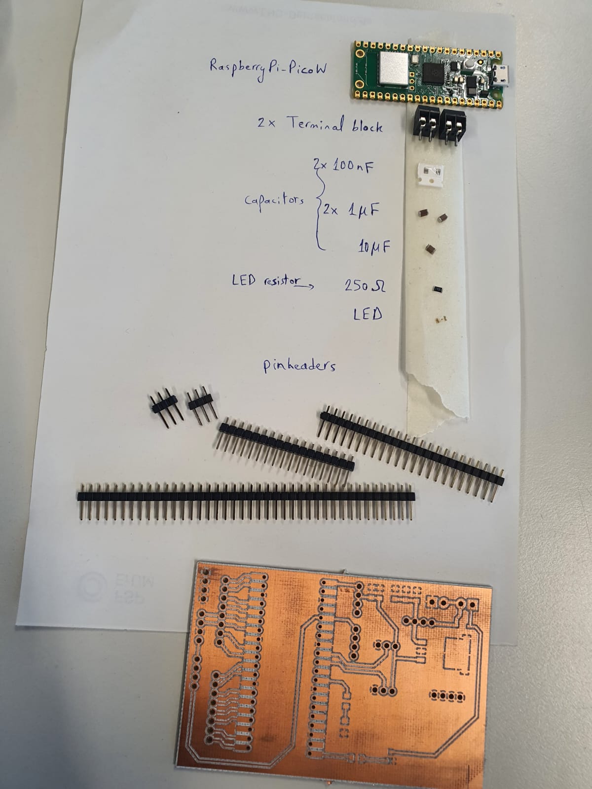
For this week, I started polishing Pi Pico–based PCB that can read a temperature sensor and drive a small DC fan via PWM for my Final Project
Datasheets for the hardware
PCB Design Modifications
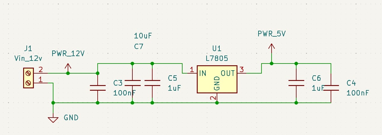
For this task, I modified alittle the board I desgined in Week
6 -Electronics Design. I added voltage regulator L7805 and I assigned footprint from
the TO-252 package existing in Fab library. Addiotnall, five capacitors are
added in parallel to filter out the voltage fluctuations (input = 12V and output = 5V).
Their values are 2 * 100nF, 2* 1uF and 1* 10uF.
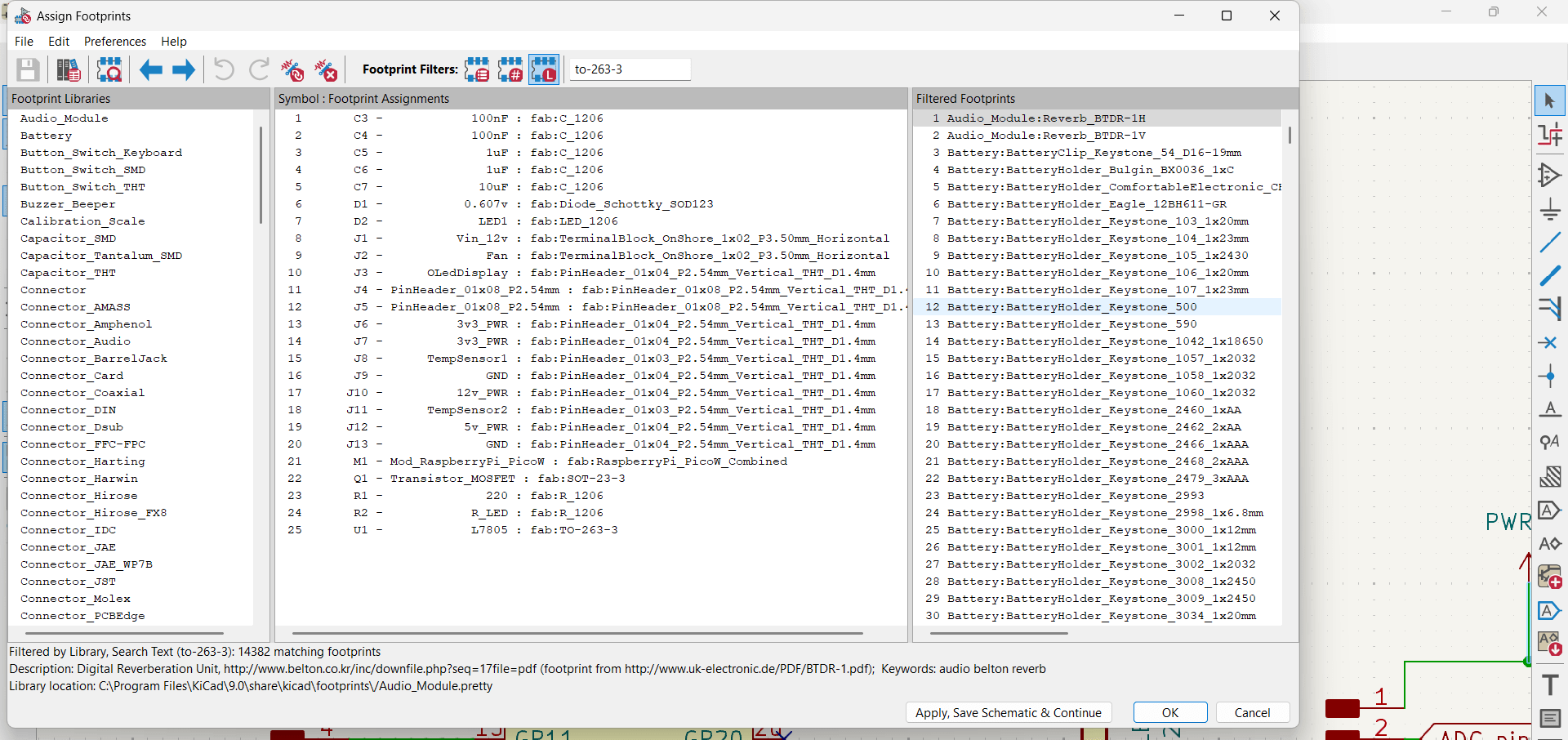
To ensure we order the right components, we check Assign Footprints. All
components we want to import their foorprints from our fab library
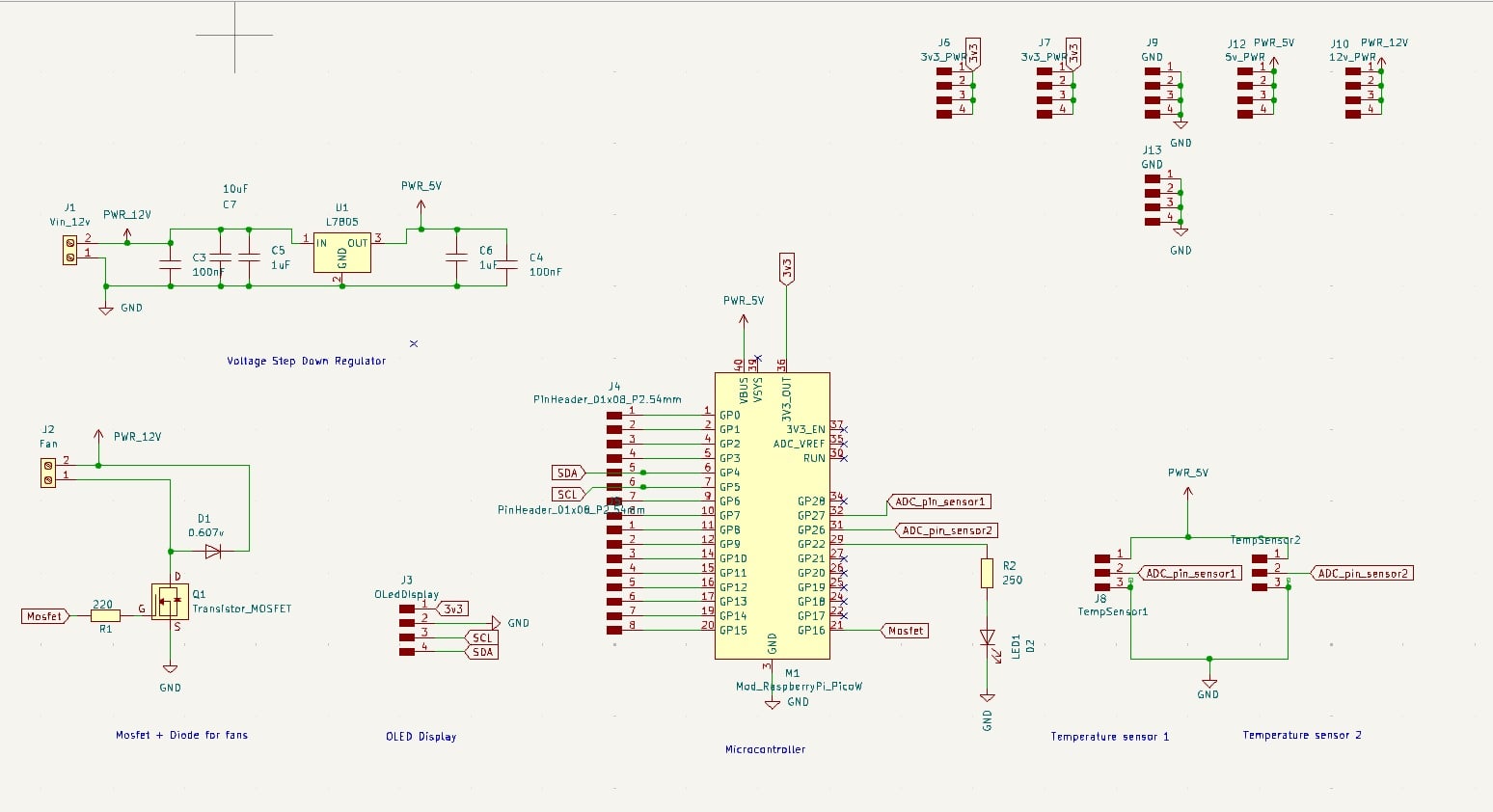
 After finalizing schematic, we switch to the PCB editor window to update
the wiring of the PCB.
After finalizing schematic, we switch to the PCB editor window to update
the wiring of the PCB.
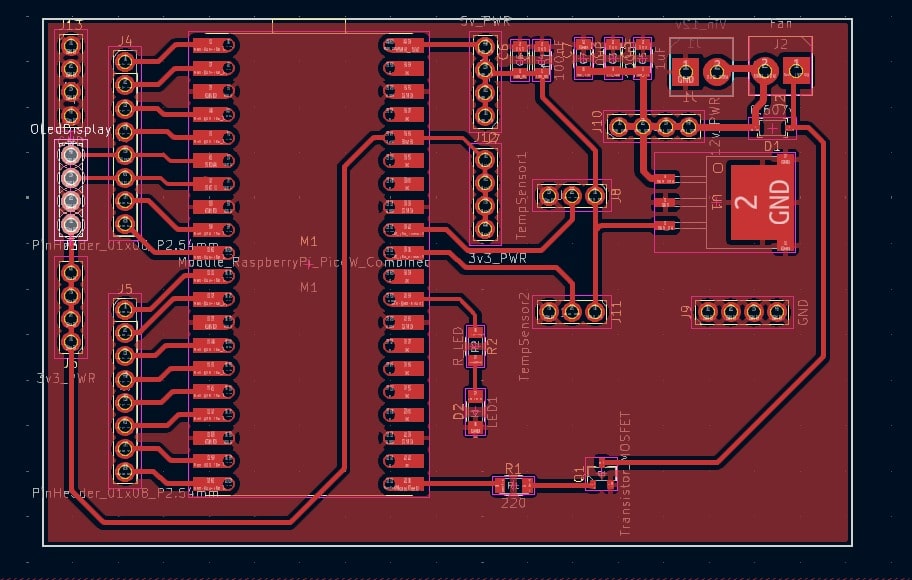 Afterwards, click on Draw Filled Zones and select GND for
layer then draw a rectangle around the PCB components. Once you are satisfied with the
draawing press b to generate the copper filled zone.
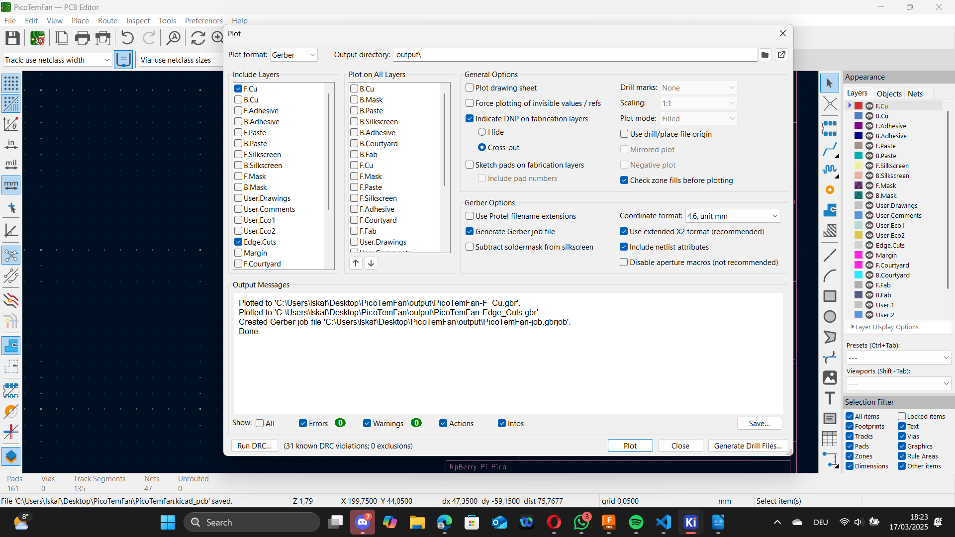
To generate Gerber files used for manufacturing PCB, go to Files > Fabrication
Output > Gerbers (.gbr). To mill the PCB later, click on
F.Cu and cut edges are sufficient. Now, set Drill Origin
to Absolute and Drill Units to Millimeter and click
generate drill files to generate files. This creates one .drill file, two
Gerber files (Edge-Cuts.gbr and F-Cu.gbr) and one Gerber Job file with a (.gbrjob).
After saving the Gerbers .zip files, they can be viewed using the Gerber
Viewer to check integrity and accuracy before sending it to the manufacturer.
Afterwards, click on Draw Filled Zones and select GND for
layer then draw a rectangle around the PCB components. Once you are satisfied with the
draawing press b to generate the copper filled zone.
To generate Gerber files used for manufacturing PCB, go to Files > Fabrication
Output > Gerbers (.gbr). To mill the PCB later, click on
F.Cu and cut edges are sufficient. Now, set Drill Origin
to Absolute and Drill Units to Millimeter and click
generate drill files to generate files. This creates one .drill file, two
Gerber files (Edge-Cuts.gbr and F-Cu.gbr) and one Gerber Job file with a (.gbrjob).
After saving the Gerbers .zip files, they can be viewed using the Gerber
Viewer to check integrity and accuracy before sending it to the manufacturer.
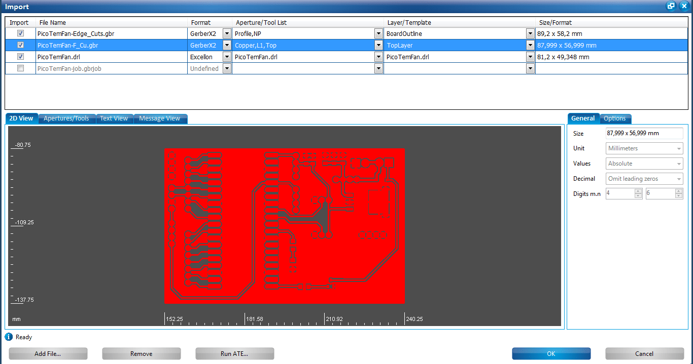
 Now, the Gerber files are ready to be sent to the PCB producer.
CAM Processing
For CAM processing, I used software called LPKF
Circuit Pro to convert the Gerber files into toolpaths.
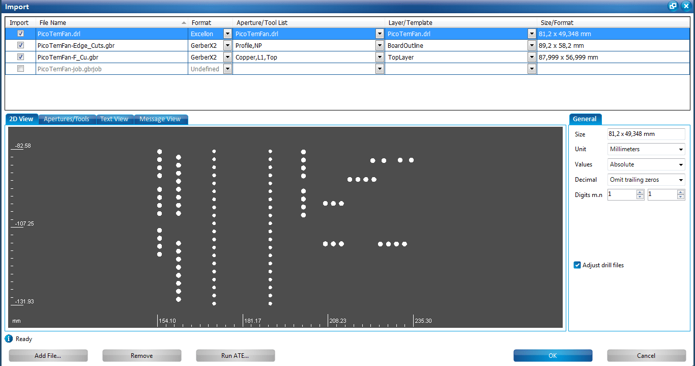
First, I opened the software and clicked on New Document and selected
Single-sided Top. Then, imported the drill and gerber files generated from
KiCad, then setting the correct parameters for
the machine starts.
To preview the traces and the drill, I pressed on the 2D view to confirm
eveyrthing is as expected from KiCAD.
Once confirmed, I was directed to the main window will show all the layers. I clicked on
Hide Empty to view only the layers relevant to my PCB.
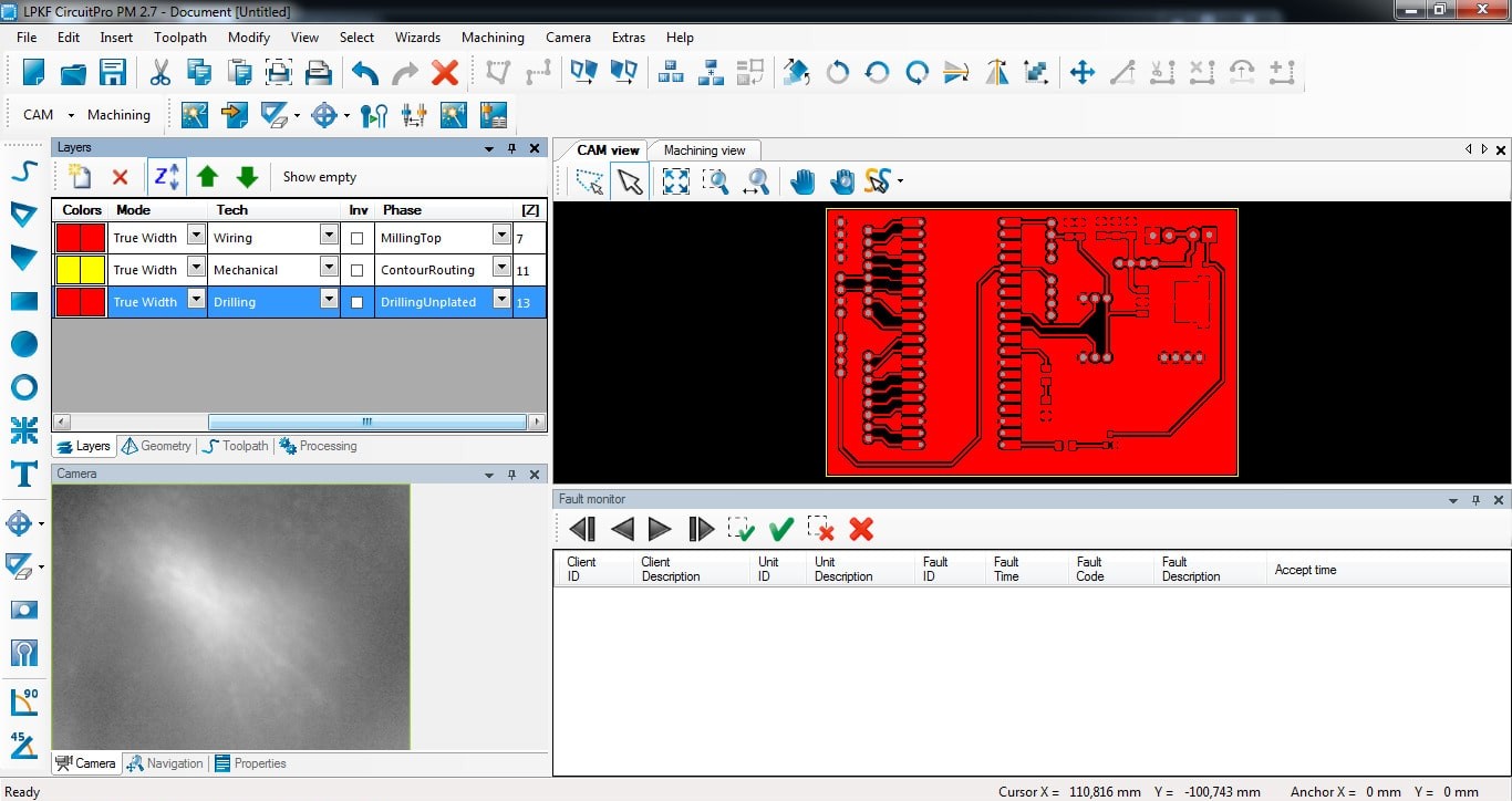
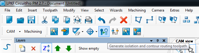
Now, I moved on to generating the toolpaths by clicking on Generate Isolation and
contouring toolpath.
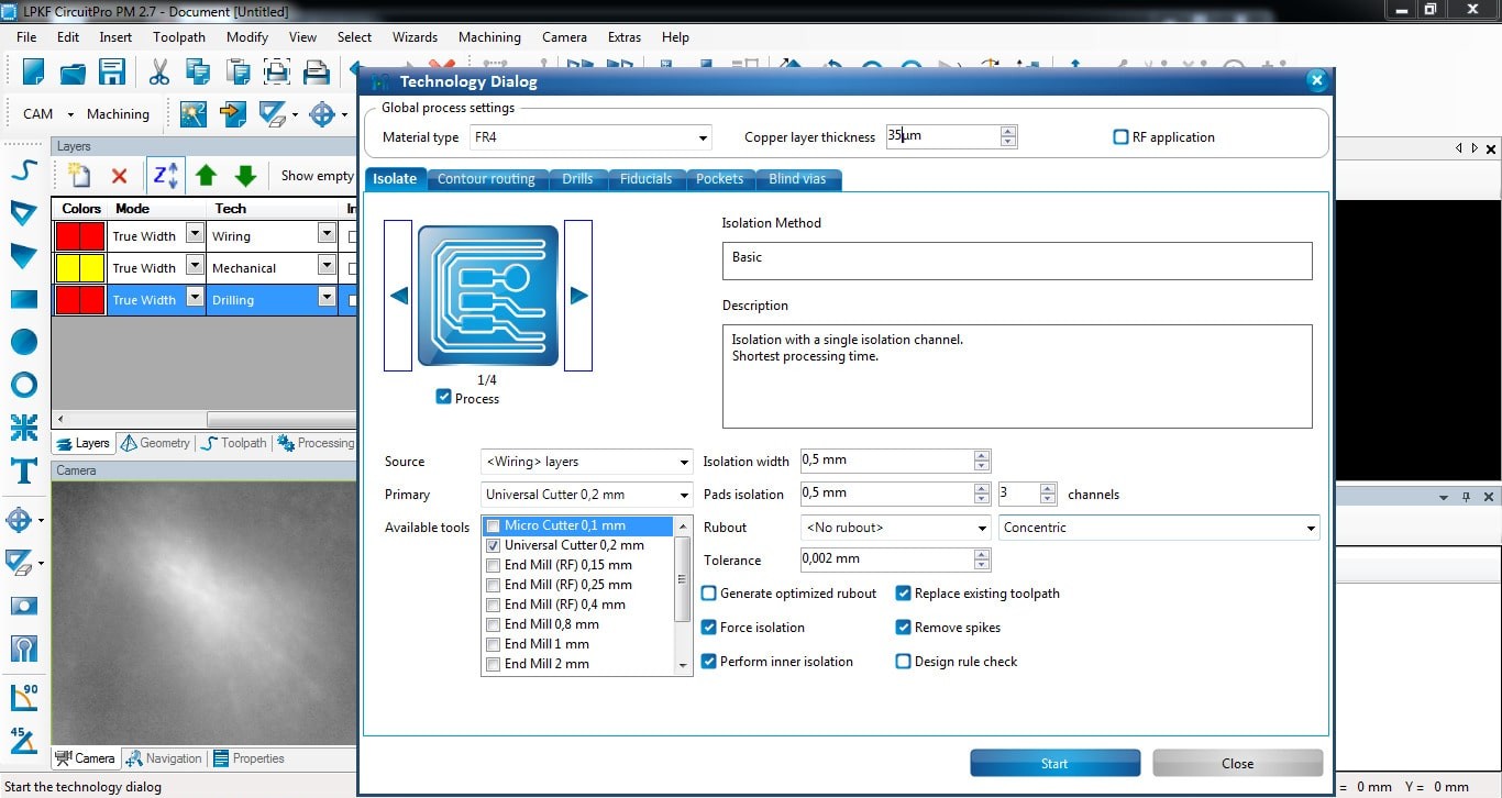
In the Isolate tab, I selected FR4 as the material type and a copper layser
thickness of 0.35 mm
For the main tool, I selected only the Universal Cutter 0.2 mm. Moreover, I
set the isolation width and pad isolation to 0.5 mm.
Next, in the Contour Routing tab, the type of the edge was adjusted to 2/6
so that the PCB stays attached on two points on each side so it does not move during the
millind process by accident on opposite ends.
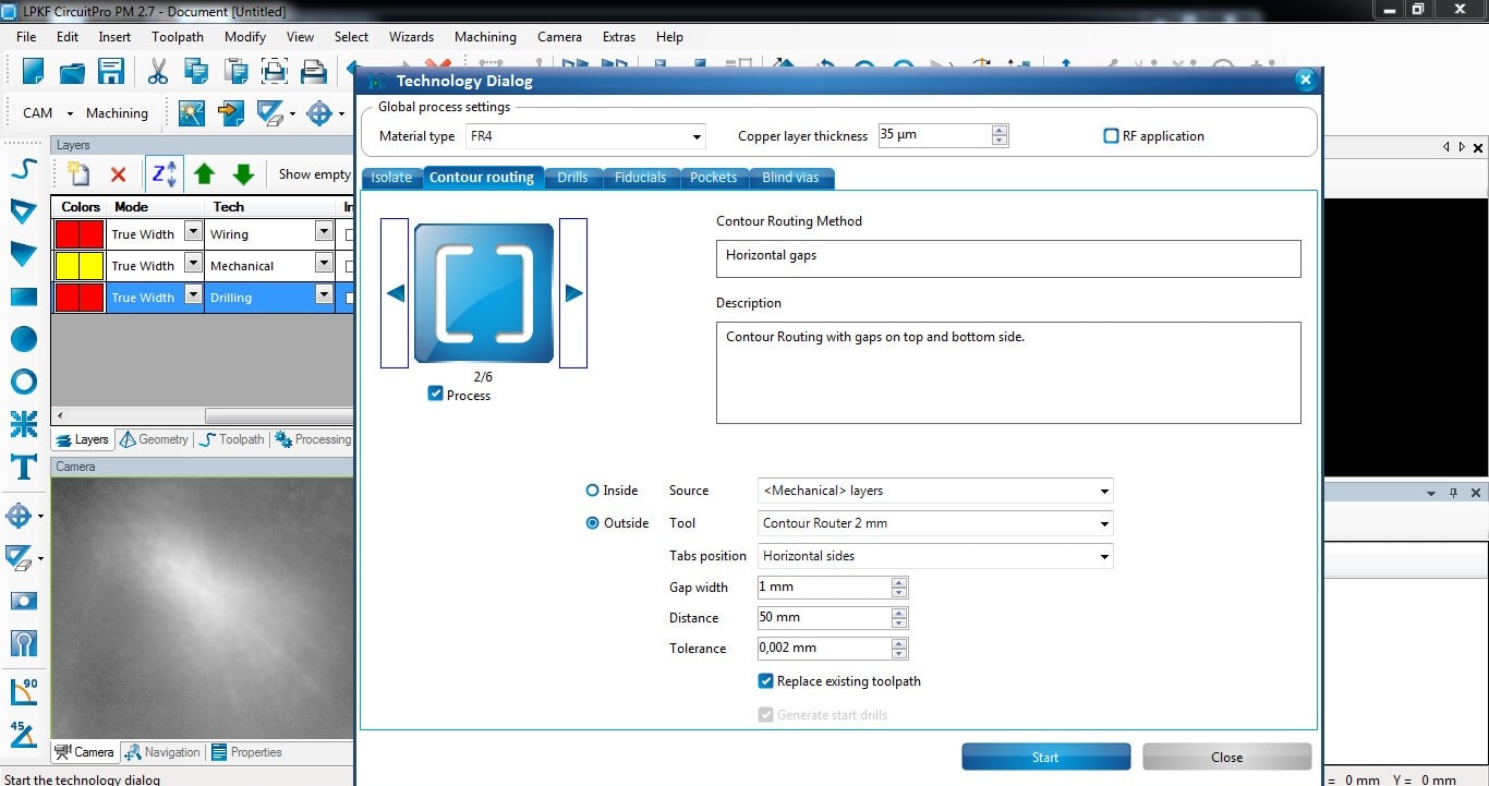
Finally, I pressed Start to determine the tools the machine should use.
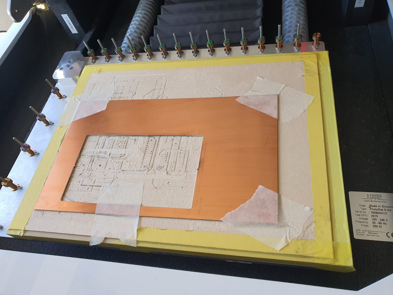
PCB Milling
The PCB milling machine I used was
LPKF ProtoMat S104 .
The same software for the processing in the previous section can also be used for the
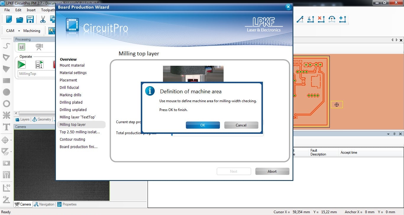
milling process. To do so, I clicked on Board Production Wizard. This
feature makes the process straightforward by automating zeroing the z-axis.
After pressing Start, I placed the copper material on top of a sacrificial
layer of dense cardboard on the bed and fixed with spaper tape.
Next, the material setting was adjusted again. The material type was set to FR4, copper
thickness to 35um and material thickness to 1.5 mm.
Moreover, the location of the material was set by clicking on the proposed bottom left
corner from the view, which moved the head of the mill accordingly. Afterwards, I pressed
the button P1. This step was repeated for the top right corner of the
material and the P2 button.
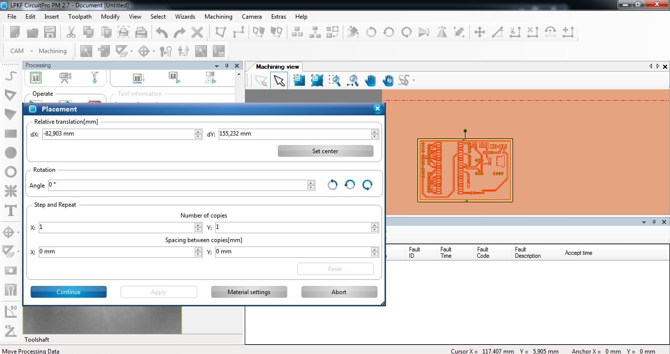
Now, the board can be placed by manipulating the Placement dialog by
dragging the PCB in the machine area view to the desired position.
Lastly, I saved the file and let the spindle heat up for few minutes to start milling the
PCB. Nevertheless, to set the depth of the milling bit, the machine is automated to do a
test cut.
Therefore, I specified in the software where it can cut the test line.
Afterwards, the software asks weather the cut is in focus. Using the camera mounted near the
head of the CNC, it can automatically adjust the depth of the V-bit.
When everything is set, milling process starts.
After the milling process, I removed the PCB from the copper material by twisting. I
furthermore used a sanding sponge to sand the copper and a fine file to round the cut edges
of PCB.
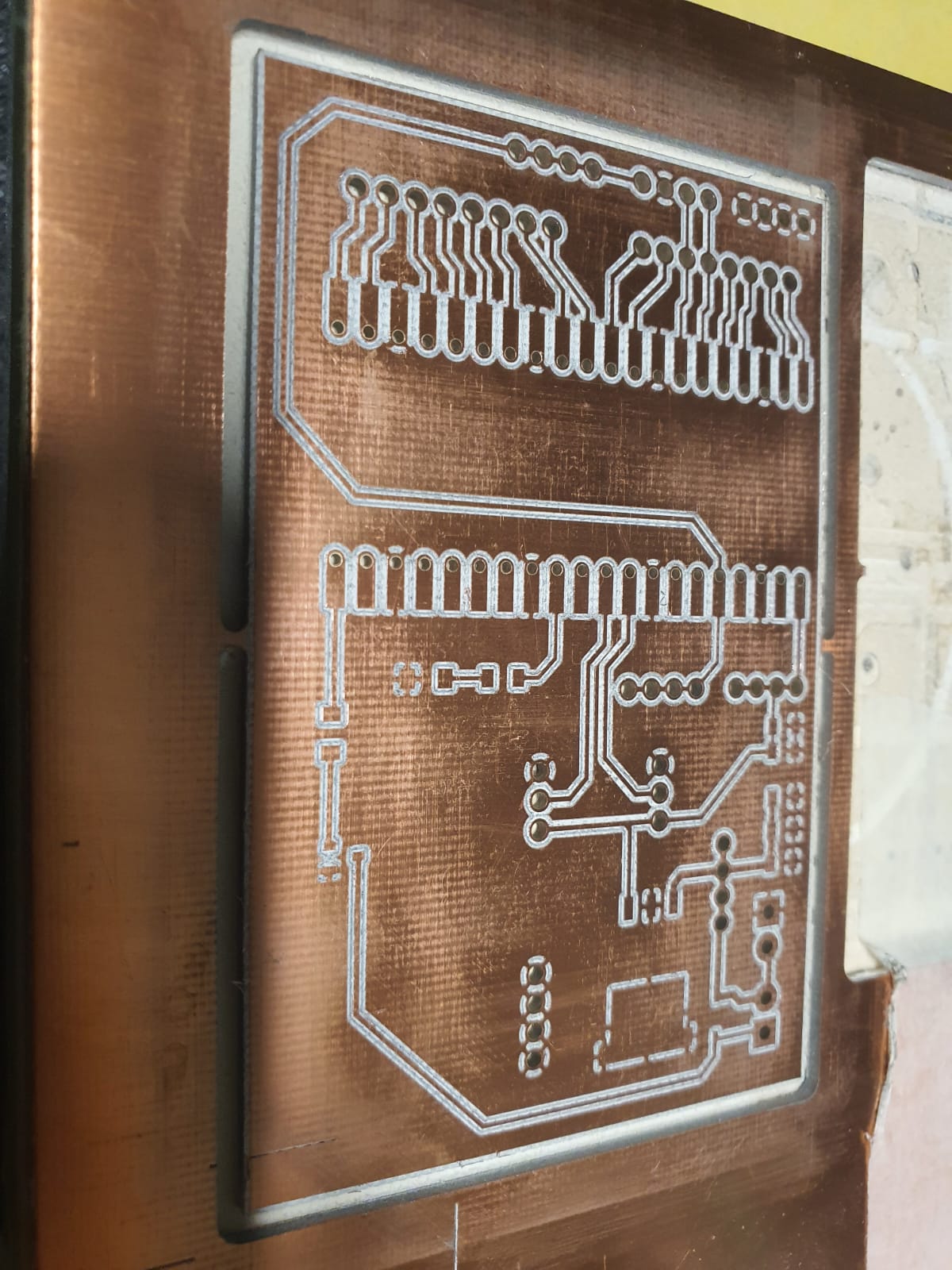
Once done, remove the tape and twist the tabs to take the PCB put of the coppoer material.
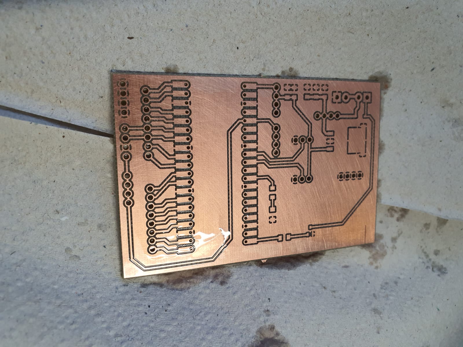
Since the copper has a UV-protective coat, cleaning it before soldering the hardware is
advised. Clean gently with a soft sponge and water to remove all the debris until it looks
shiny.
Finally, next step comes, which is soldering the hardware components. However, diode and
mosfet were ordered today and still need to arrive to solder them for the Final
Project.
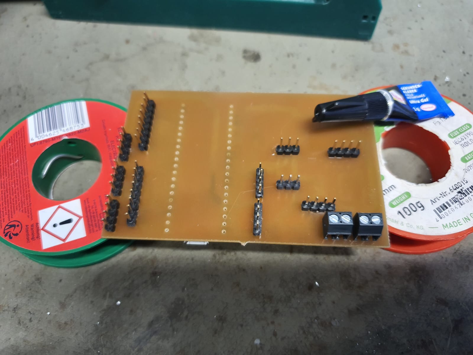
PCB Soldering
Before moving on the soldering, we went and collected all the components that I need to
solder and taped them on a paper tape and annotated them accordingly. This makes the
soldering process more straightforward.
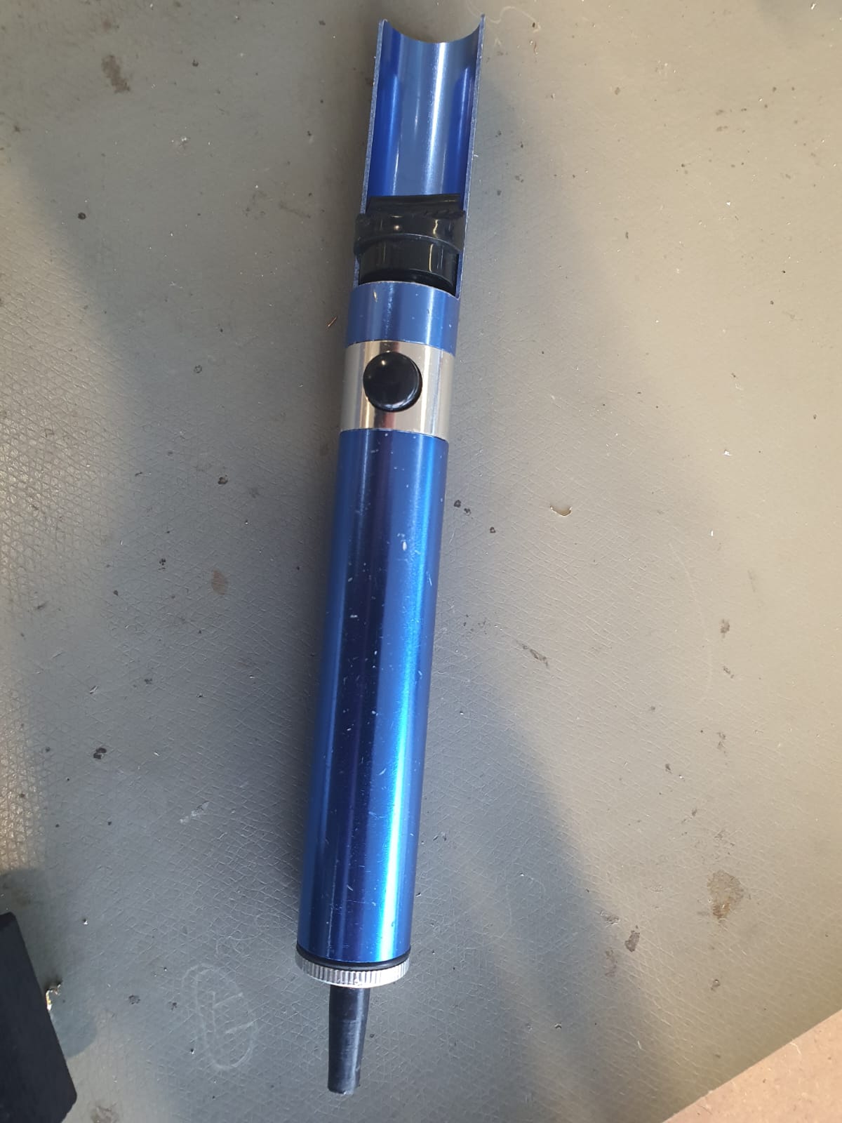
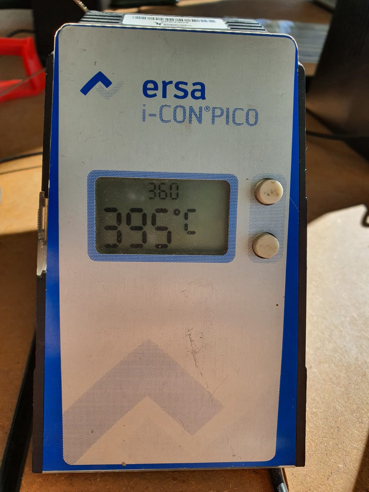
 For PCB soldering, I used a manual soldering station. The station is composed of soldering
iron, with a handle and a stand, and a soldering base that is used to manipulate the
temperature. To clean the tip of the soldering iron between each time, metal wool is
typically used.
For PCB soldering, I used a manual soldering station. The station is composed of soldering
iron, with a handle and a stand, and a soldering base that is used to manipulate the
temperature. To clean the tip of the soldering iron between each time, metal wool is
typically used.
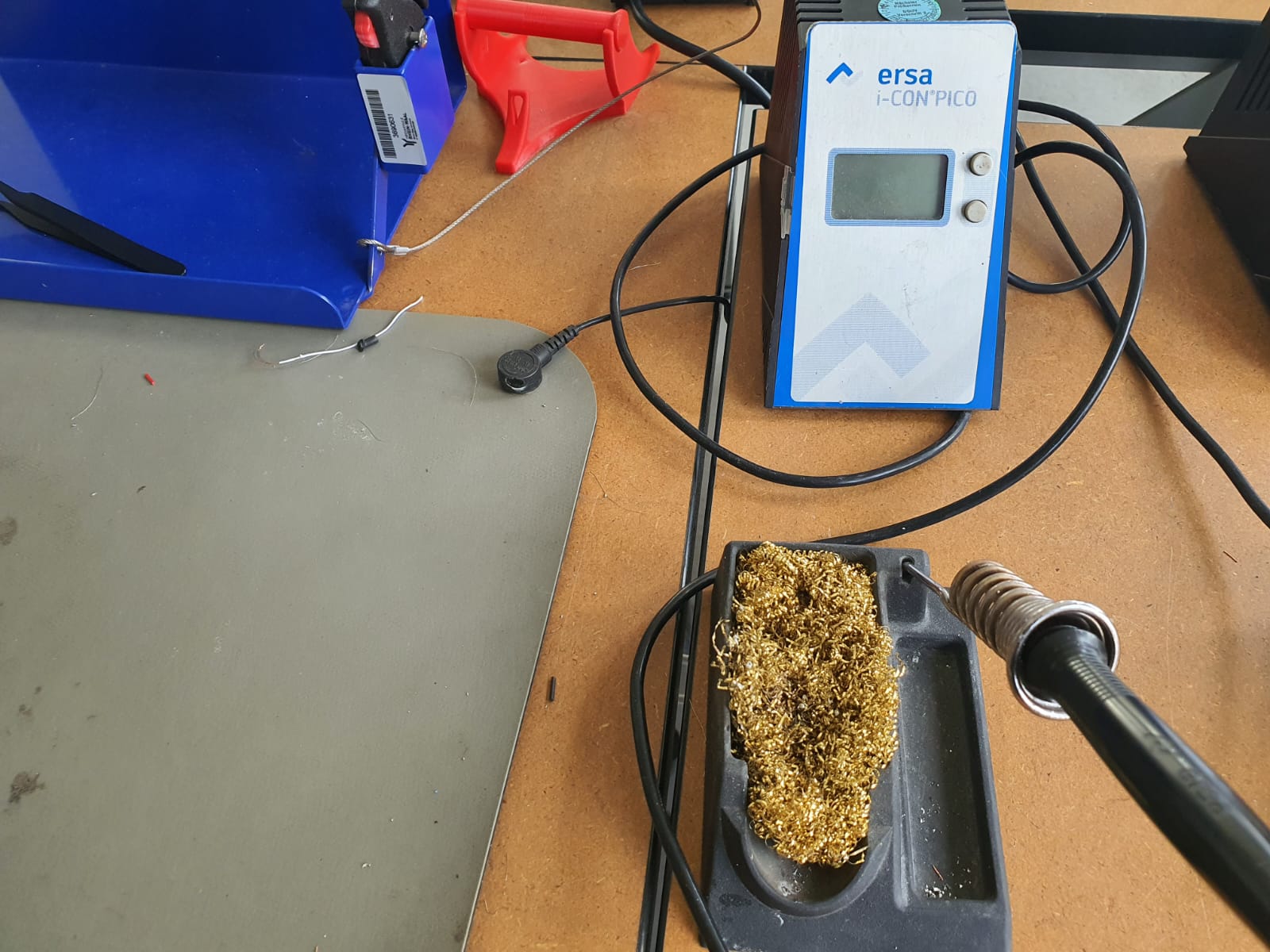
Nevertheless, since we did not know who used it first, we cleaned it with some solder
tip cleaning paste before starting to solder to make sure evrything melts and forms
joints properly
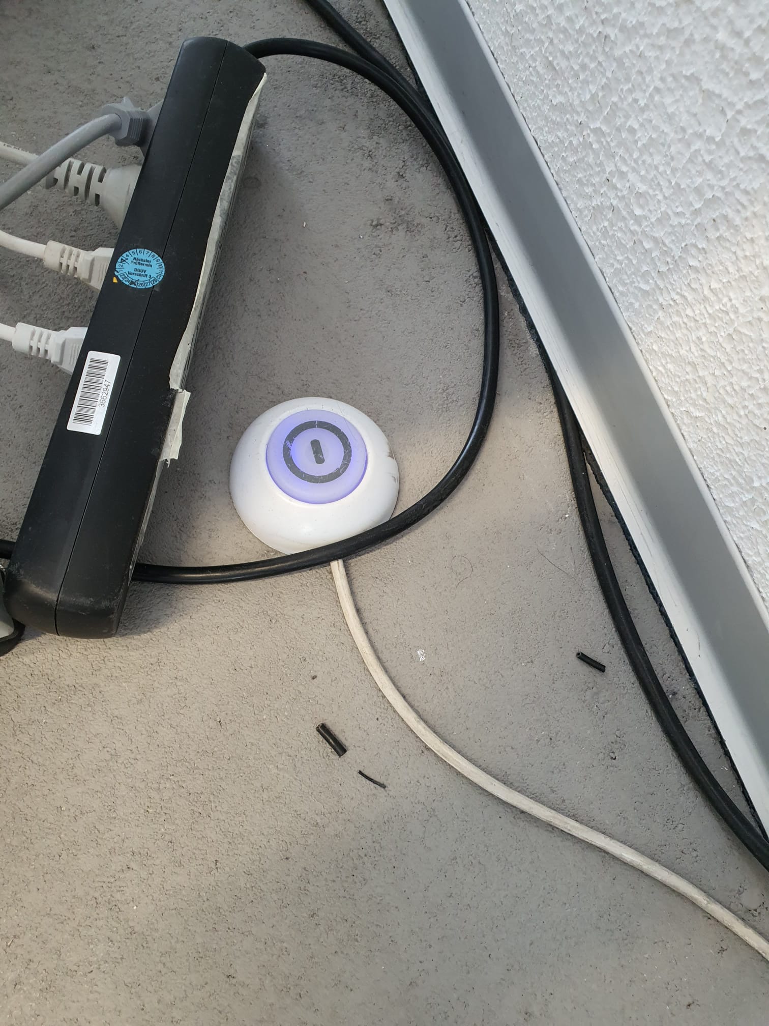
For safety purposes, a fume extractor should always be placed close to the soldering
location, since melting the solder material can emit toxicant fumes that are dangerous
to humans' health.
To start the extraction, step on this button!
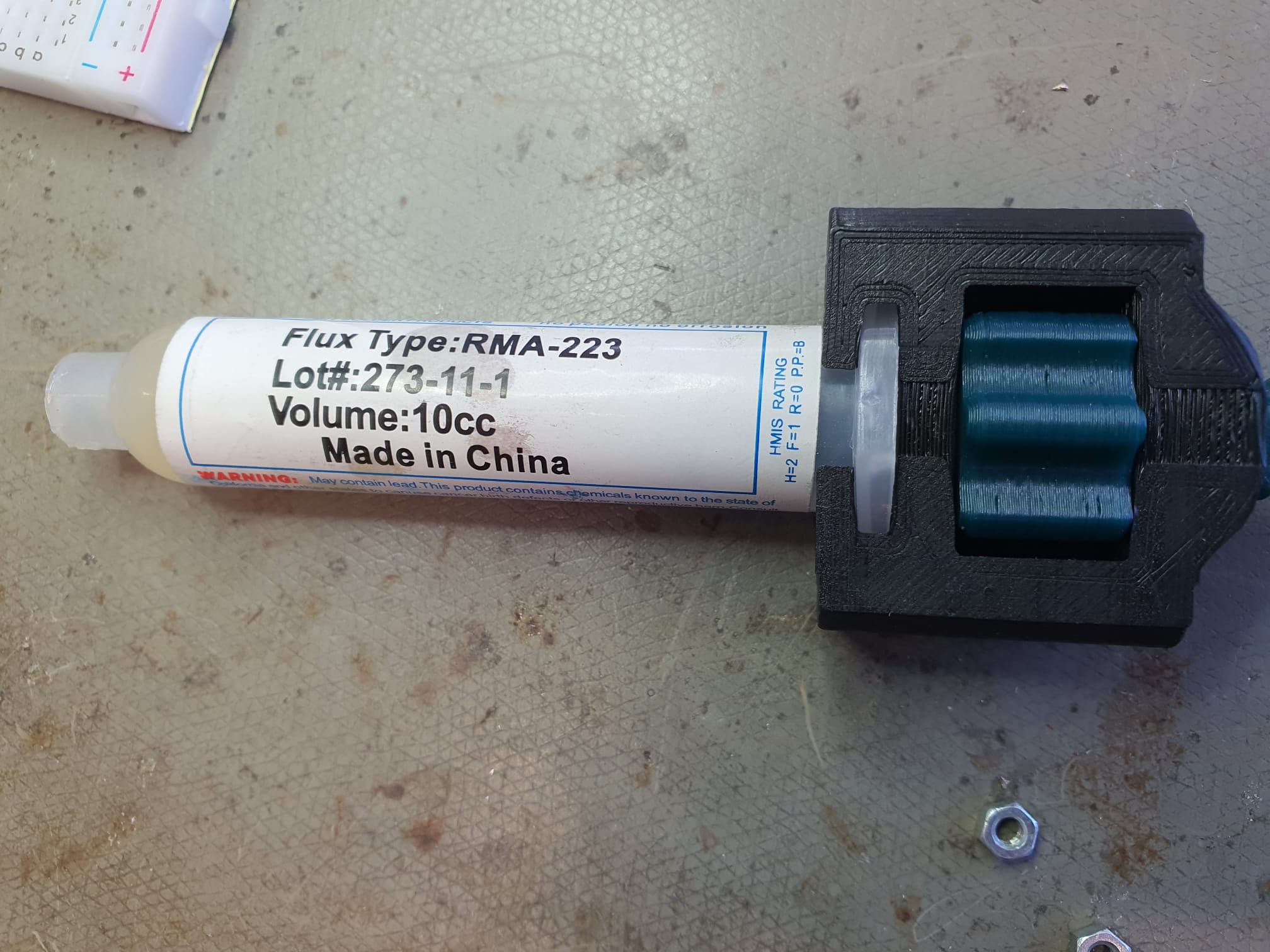
To make sure that the joints are properly established, adding flux using this flux
injector is recommended.
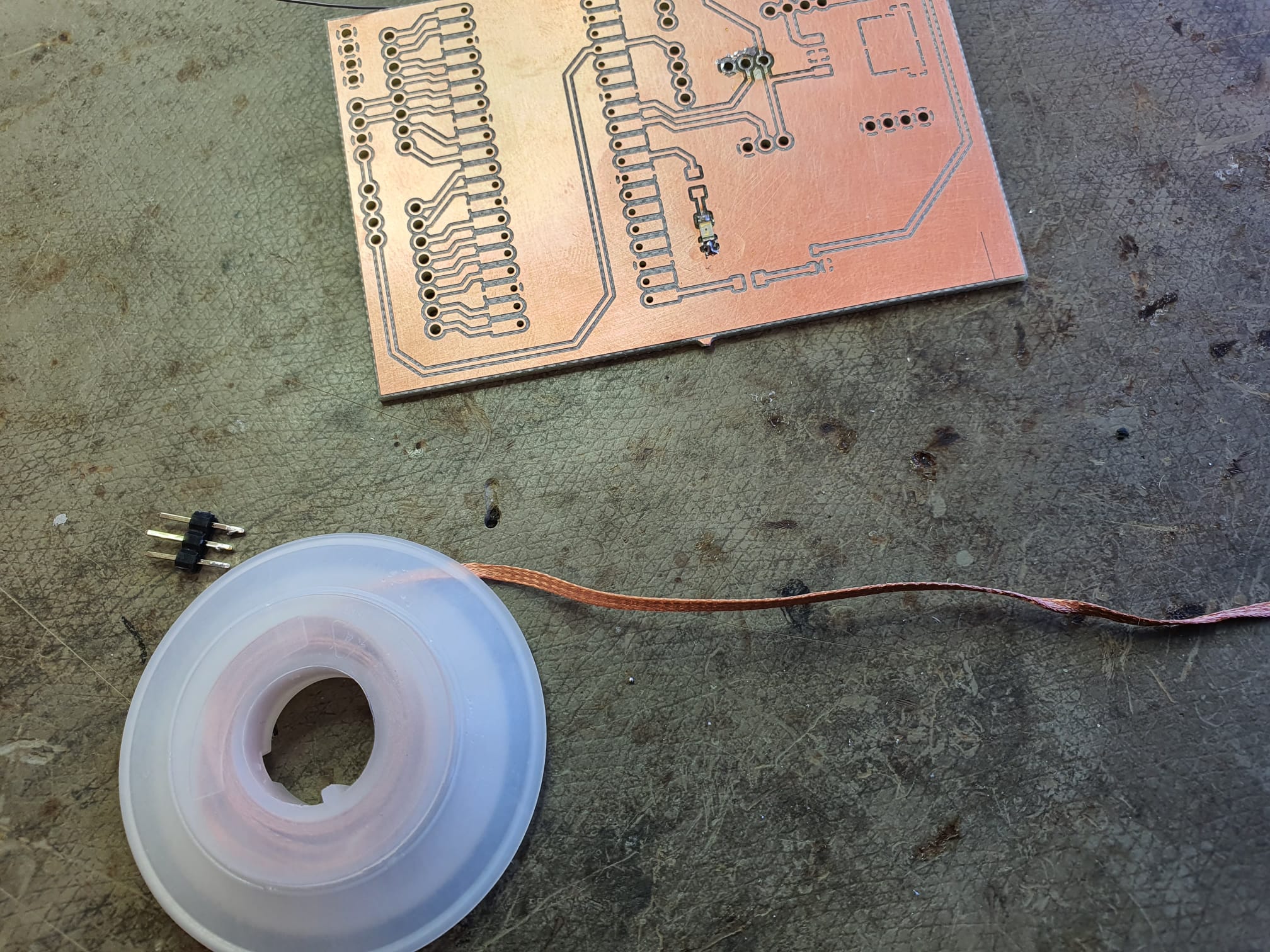
Moreover, solder material suction or solder removing tape mecahnism can be used to fix
bridging between points that shoul not be connected or to restart the soldering freshly.
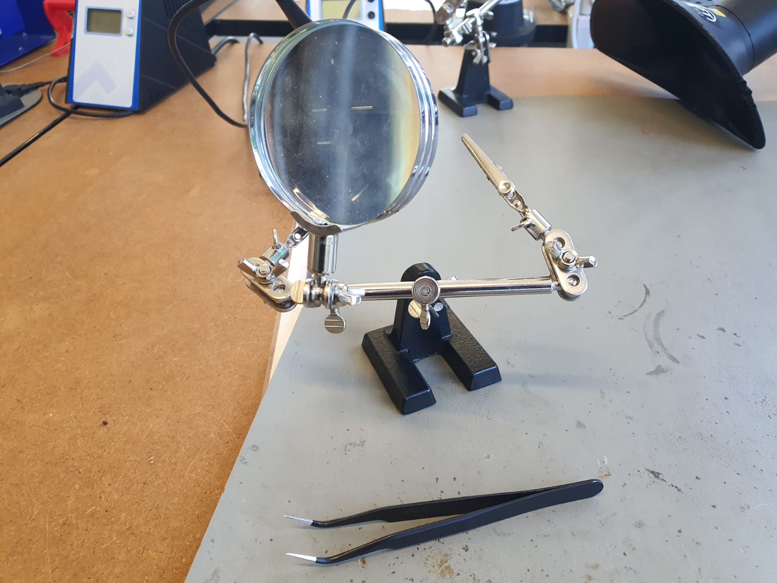
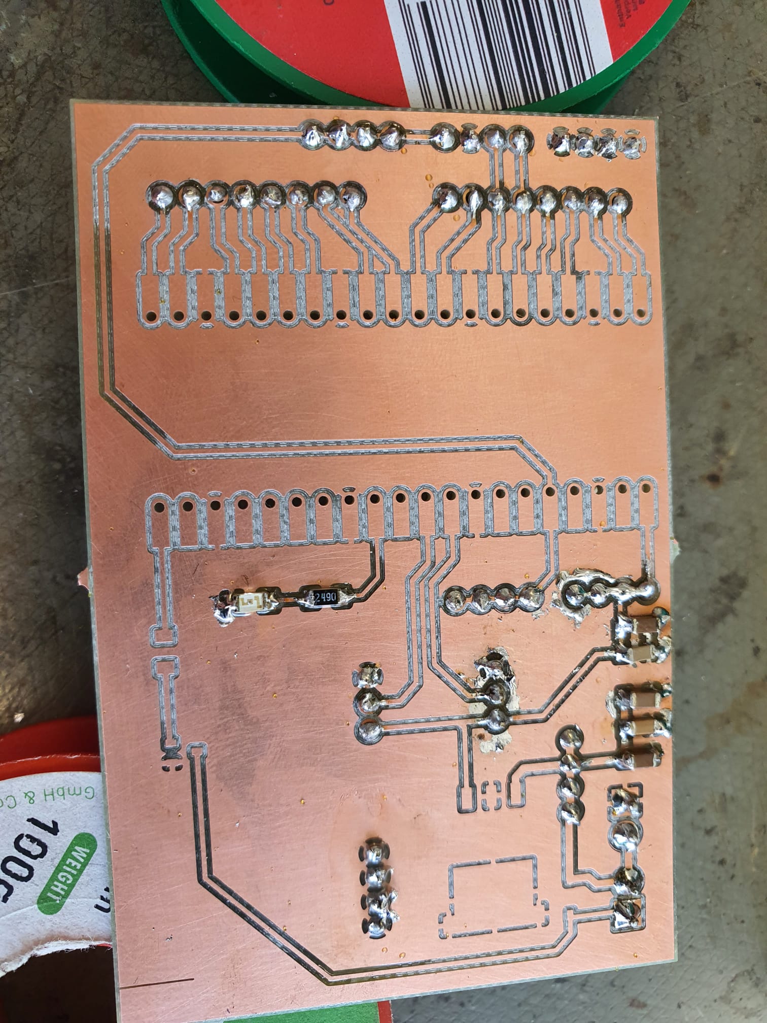
All of the components I soldered were surface mount technology (SMT), except for the pin
headers, which were through-hole technology (THT). Mounting components to the surface is
relatively easy.
To connect easier, I first melted some solder onto the pad. Then, the component was
pushed gently in position using a tweezer. Iron solder temperature is very important; if
too high then it might leave a burn mark on the electronics, if it is too low, it might
not even melt the solder tin. Thus, few attempts have to be made in order to get the
feeling of which temperature works best for your own pace.
Sometimes placement adjustments have to be made to align components properly. This was
done by heating the solder tin to be melted again, and this, enables re-positioning.
Once the component is fixed in the desired position on the first solder pad, the
remaining pins can be soldered.
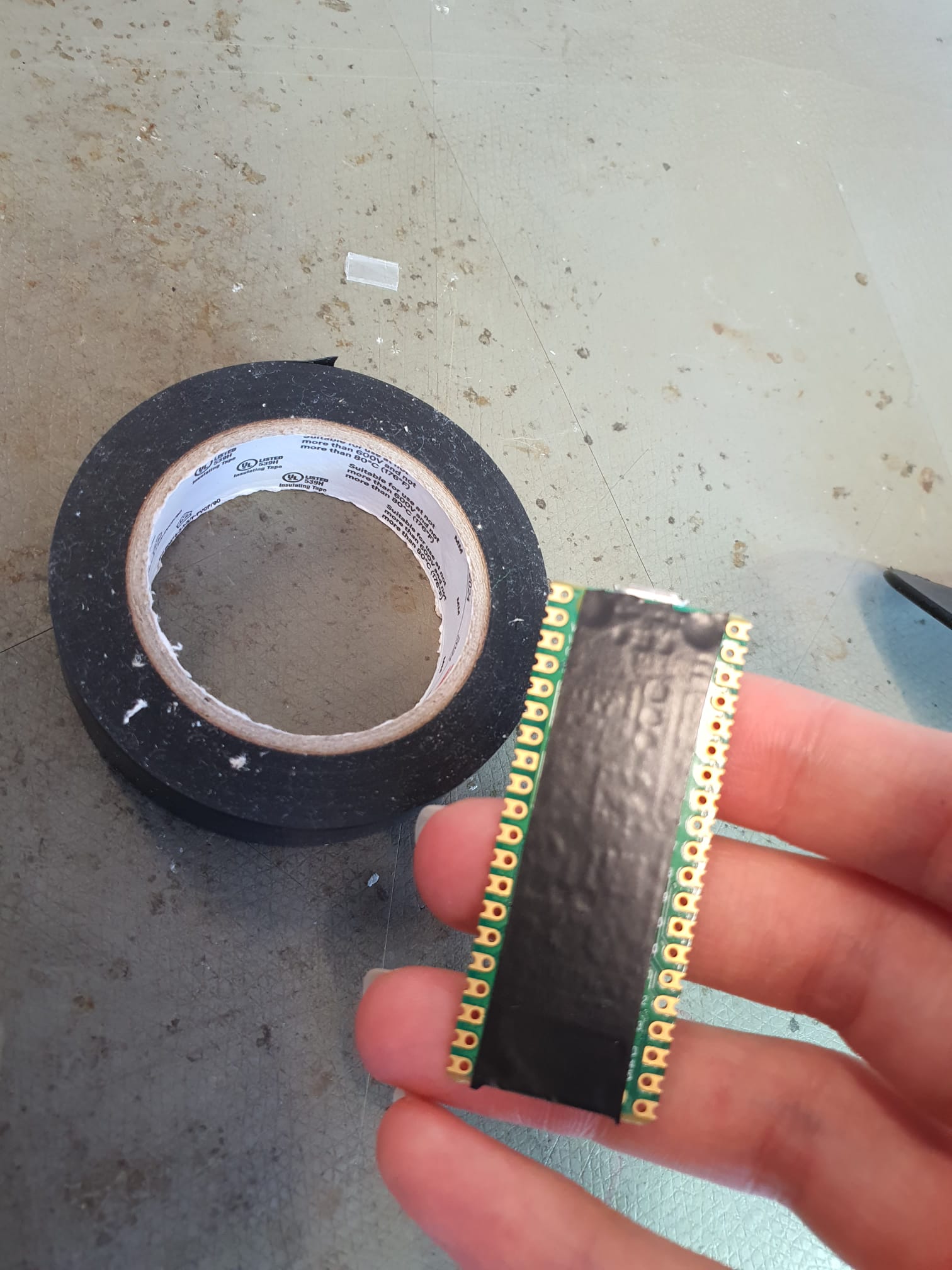
For THT components (pinheaders), they are inserted through muliple holes and solder is
applied on the other side. This was quite tricky because the PCB had to be positioned
alittle elevated to be able to fit the other side of the headers. Moreover, making sure
that they are perpendicular was quite challenging because they were first soldered
inclined and had to be readjusted every single time.
To solve this I improvised a stand made of to tapes, then I flipped the board and add
tiny spot of glue to fix the pinheaders as flat and vertical as possible relative to the
PCB itself. Aftey drying, I flipped the board again and managed to solder the pinheaders
straightforward afterwards!
With time passing by and having soldered more and more components, my technique of
synchronizing the component-solder tin- solder iron sequence and timbing was improving.
The best practice is to create a cone-shaped and shiny solder joints. Additionally, if
when the joints are dull, the solder iron should heat up the tin again to head the
solder up once more.
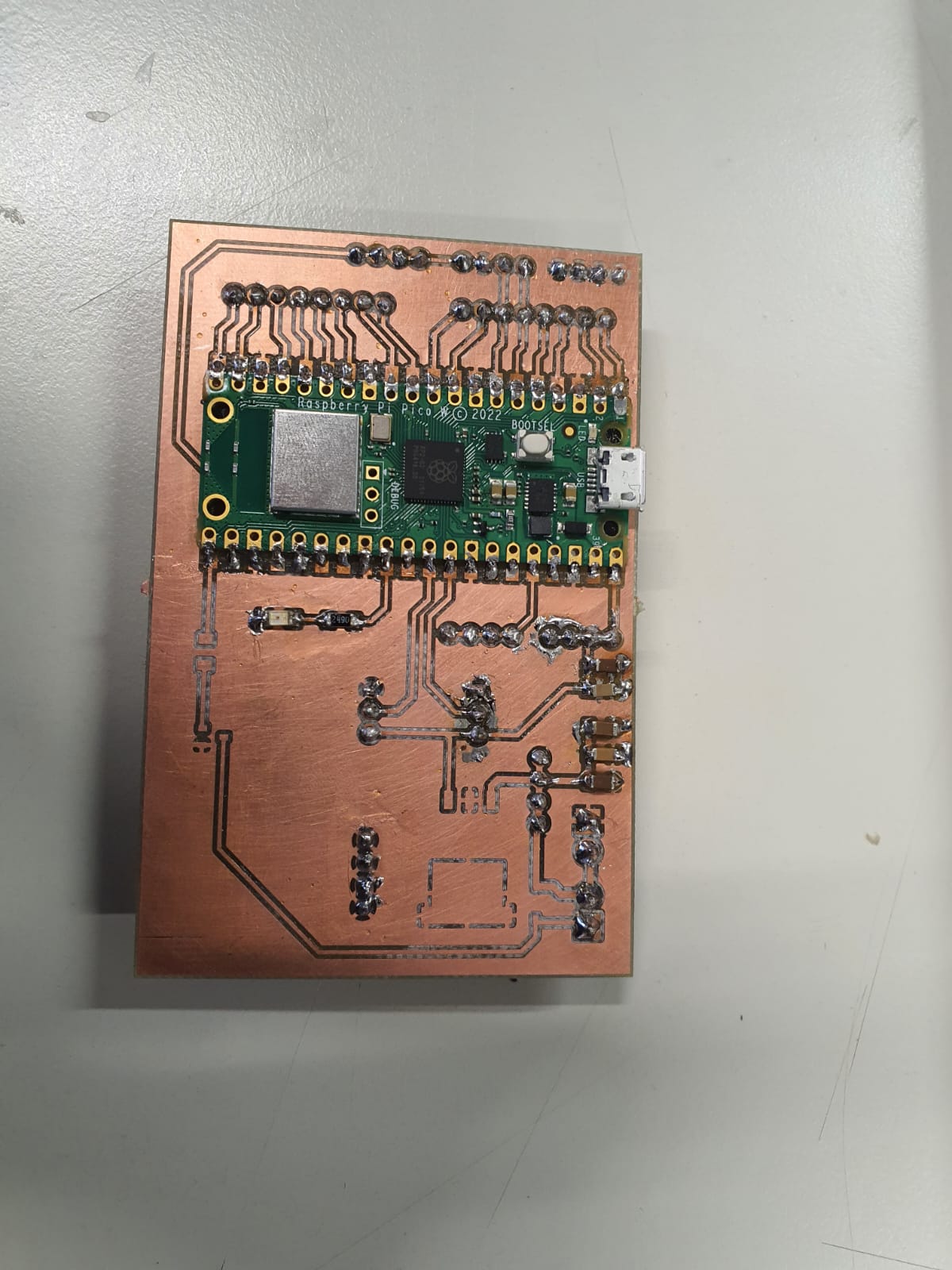
To solder the microcontroller at the end, I added an insulation tape to protect all of
the tiny components the Pico has and insulate them from GND.
Then I had to make sure it aligned with the holes properly by pushing and maneouvering
with the tweezrer, starting from the upper right pin pad, moving down, then soldering
the other side.
You can see that I started soldering process with the capacitors at the upper right
corner of the PCB, then moved to resistor and pinderheard, and lastly the
microcontrollers. My skills got visibly better by the end of the process.
Nevertheless, few times I had to resolder certain spots because I created by mistake
bridging to GND where it should not bridge, which was alittle tougha t the beginning,
but it became more straightforward once I managed to hold the solder tip in the right
way and I heated up properly the pad and the component before inserting the tin in
between.
Tip: your solder tip must be horizontal, so you get
the maximum surface contact area and the point you are trying to solder is heated
properly!
All in all I was quite content with how the PCB turned out. Few components are missing
but now I can solder components more efficiently and quickly with this practice.
PCB Testing
Following the steps presented in this link,
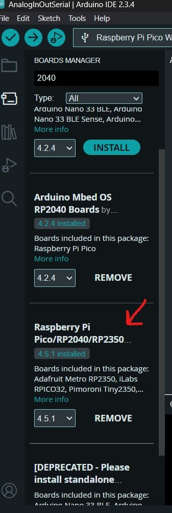
I downloaded the right library manager for the micrcontroller (RpBerry Pi Pico W).
Blink LED example:
From the video below, we can see that the on-board LED is turning on and off at regular
intervals of one second. This proves that the microcontroller's Blink LED code is
working as intended. The steady blinking and the time interval show that the PCB's
digital output is undamaged and the delay is accurate.
Therefore, we can indirectly confirm that the PCB layout and component soldering are
properly done.
                        /*
                          Blink Modified

                          Turns an LED on for one second, then off for one second, repeatedly.

                          Most Arduinos have an on-board LED you can control. On the UNO, MEGA and ZERO
                          it is attached to digital pin 13, on MKR1000 on pin 6. LED_BUILTIN is set to
                          the correct LED pin independent of which board is used.
                          If you want to know what pin the on-board LED is connected to on your Arduino
                          model, check the Technical Specs of your board at:
                          https://www.arduino.cc/en/Main/Products

                          modified 8 May 2014
                          by Scott Fitzgerald
                          modified 2 Sep 2016
                          by Arturo Guadalupi
                          modified 8 Sep 2016
                          by Colby Newman

                          This example code is in the public domain.

                          https://www.arduino.cc/en/Tutorial/BuiltInExamples/Blink
                        */

                        // the setup function runs once when you press reset or power the board
                        void setup() {
                          // initialize digital pin LED_BUILTIN as an output.
                          pinMode(22, OUTPUT);
                        }

                        // the loop function runs over and over again forever
                        void loop() {
                          digitalWrite(22, HIGH);  // turn the LED on (HIGH is the voltage level)
                          delay(1000);                      // wait for a second
                          digitalWrite(22, LOW);   // turn the LED off by making the voltage LOW
                          delay(1000);                      // wait for a second
                        }
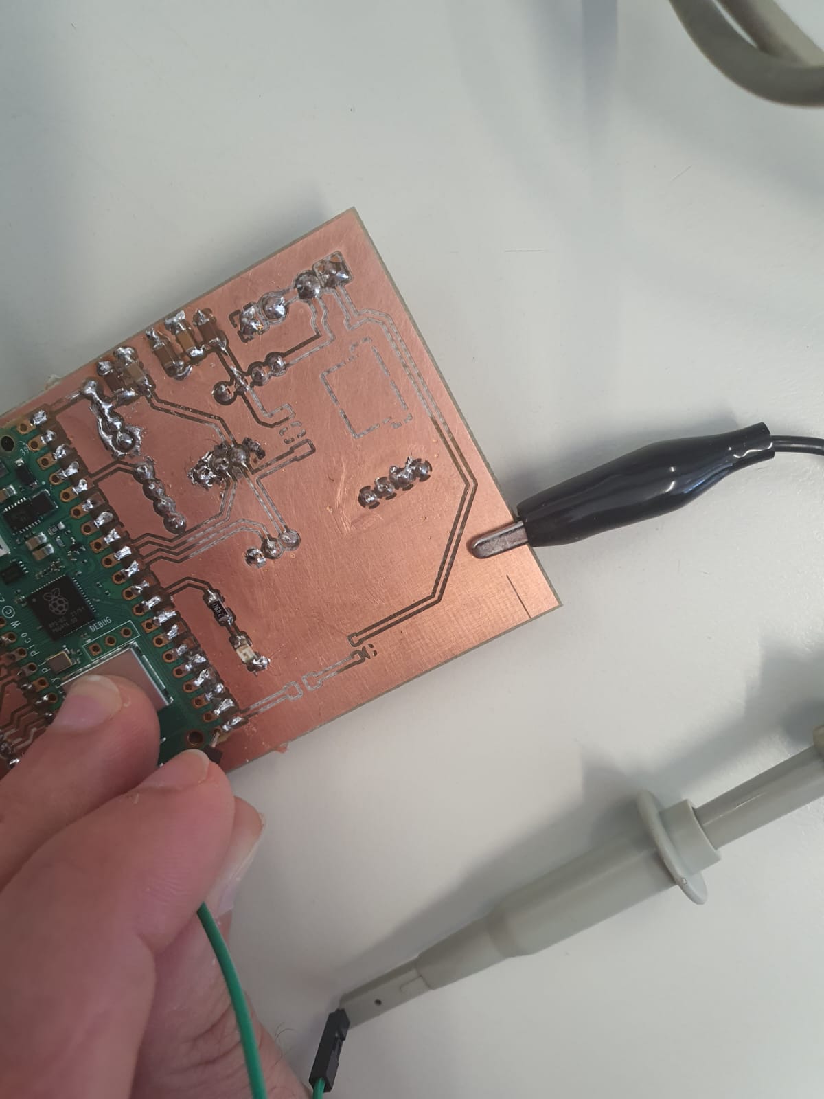
Multimeter Test for the Mosfet pin (pin 22):
In the video below, we used a multimeter to test voltage levels at different points on
the PCB.
This can help us check if there is any bridging between two pins that should not be. GNG
should be basically everywhere on the material and the multimeter should beep when
touching it with its negative (black) side.
To check the voltage end, we can connect and uplaod the code that writing analog output
into the mosfet-to-be pin (pin 16). Reading 3.3v on the multimeter also confirms for us
that voltage measurement is accurate and stable where it is supposed to be.
Oscilloscop Test for the Mosfet pin (pin 22):
One last test to perform was with the oscilloscope we used in our Group
Assignment-week 6. This device can record the PCB's output in a waveform .
High (3.3v) and low (0v) voltage levels are clearly transitioned in the waveform in the
the form of the duty cycle.
Applying the same code as for the multimeter test and varying the output from 0 to 255
could should us different duty cycles that will be controlled by the mosfet to drive the
fan in different speeds, which is what we call Pulse Width Modulation PWM.
This is a technique where the digital signal controls the average power delivered to a
device (in our case fan) by varying the width of pulses in a fixed period.
The results shown in the video confirm that the pin actually can drive PWM, so we
selected the right pin for the mosfet-fan components.
        /*
        PWM - Mosfet Pin Test- modified from Blink Example


      // the setup function runs once when you press reset or power the board
      void setup() {
        // initialize analog pin as an output.
        pinMode(16, OUTPUT);
      }

      // the loop function runs over and over again forever
      void loop() {
        analogWrite(16, 200);  // Range from 0 to 255 to show varying voltages and duty cycles
                           // wait for a second
      }
Conclusion and Reflection
In summary, I learned how to characterize design rules, generate toolpaths, mill a PCB,
solder hardware components. Moreover, I tested my own PCB using a test code I am
developing slowly for my Final
Project.
My technical skills and problem-solving abilities have improved as a result of
overcoming obstacles, especially when it came to soldering.
However, I can say that I am now more comfortable managing PCB fabrication tasks, and I
am looking forward to complete my PCB for my Final Project because this assignment
overall was very fun :D
Files
- PCB Design
- PCBDesign.zip
- PCB Test Code - LED Blink
- BlinkPCBTest.ino
- PCB Test Code - PWM Mosfet Pin
- PWMPinPCBTest.ino