Electronics Production
Electronics Production refers to the process of developing, assembling, and manufacturing electronic
devices and components. Electronic design and production, material procurement, assembly, testing, and final
packaging are some of the steps in this process.
Electronic manufacturing services (EMS) companies are businesses that specialize in providing these services.
The Printed Circuit Board (PCB) is the building block of the majority of electronic devices. Moreover, crucial
parts like resistors, capacitors, and microprocessors are connected by the PCB. These components are installed
utilizing methods like Surface Mount Technology (SMT) or Through-Hole Technology (THT). Before the finished
product is sent to customers, these parts are assembled and put through a rigorous testing process to
guarantee high quality and dependability.
- Characterize the design rules for your in-house PCB production process
- Send a PCB out to a board house
LPKF ProtoMat S104
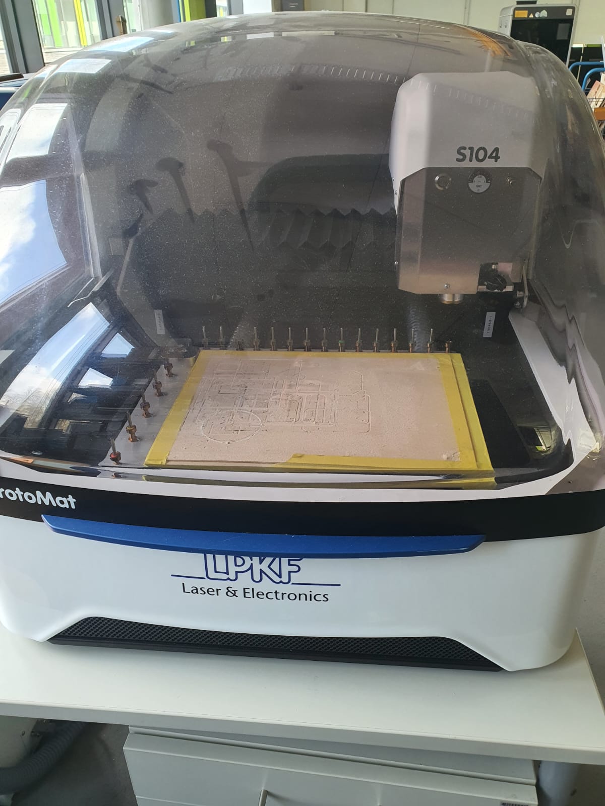
In our Fablab in Kamp-Lintfort, there is an operating CNC milling machine for milling PCBs called LPKF ProtoMat S104 and we selected this one to characterize the PCB manufacturing process
LPKF ProtoMat S104 Test
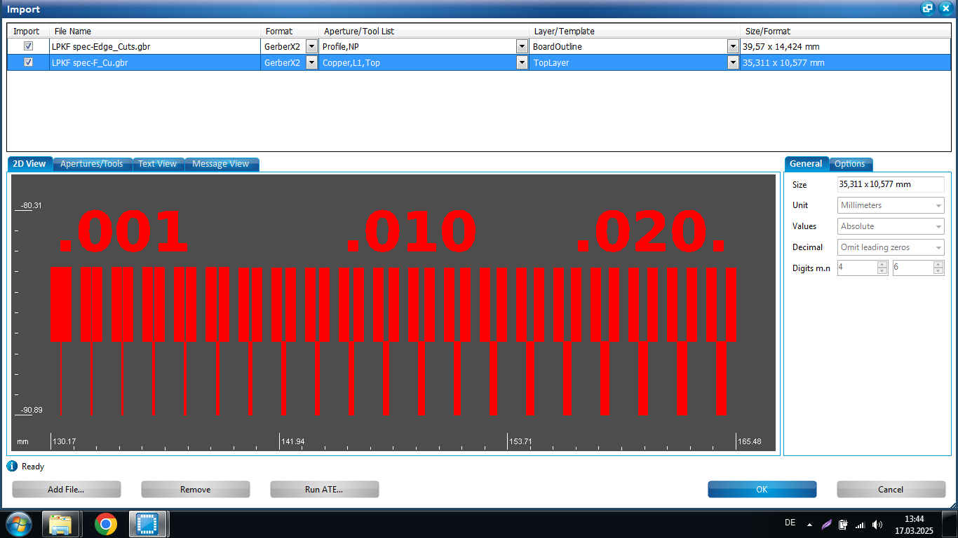
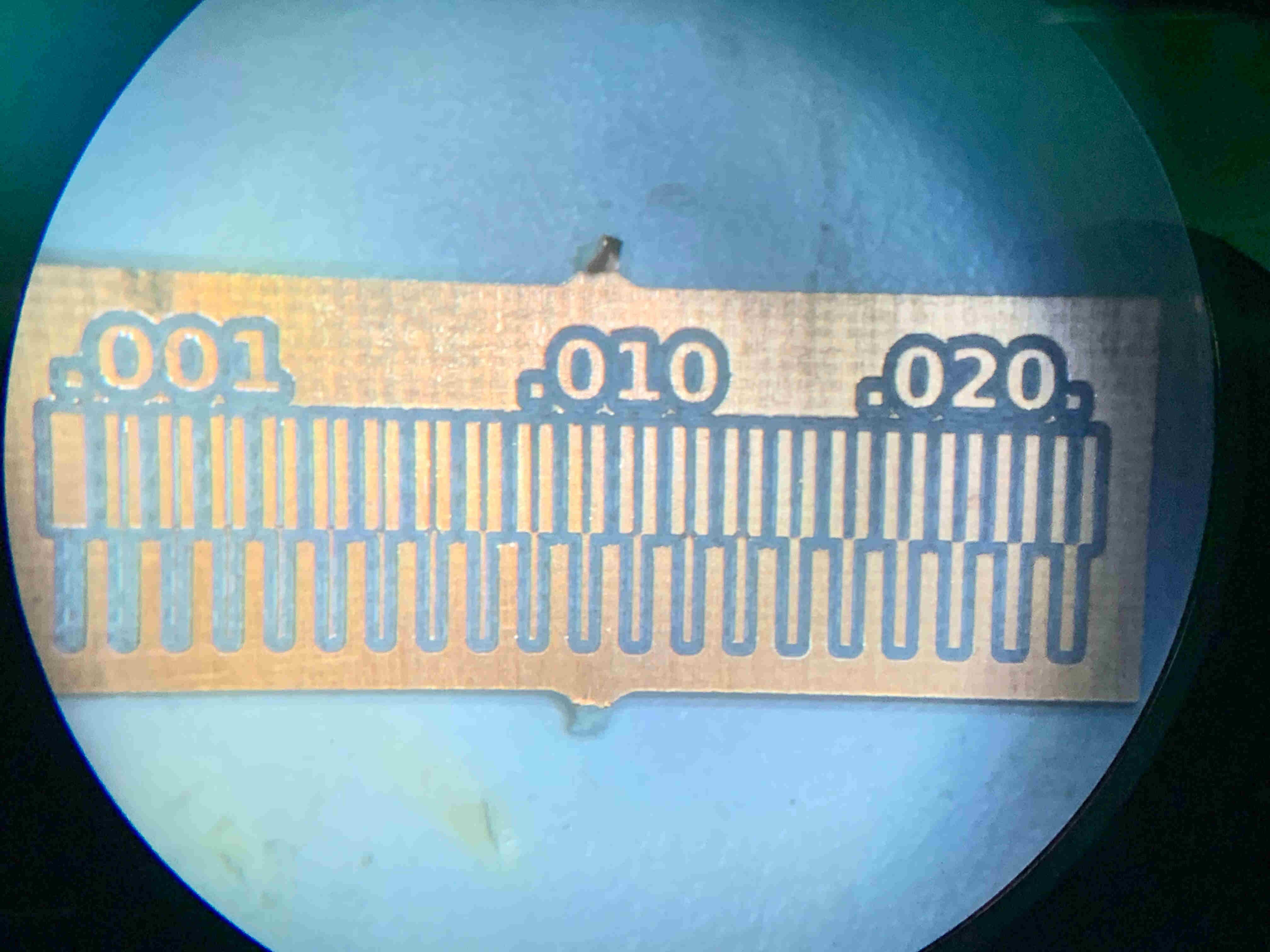
To test the thinnest trace and the clearance that the LPKF can make, we imported two Gerber test files for a comb-like PCB with varying isolation widths.
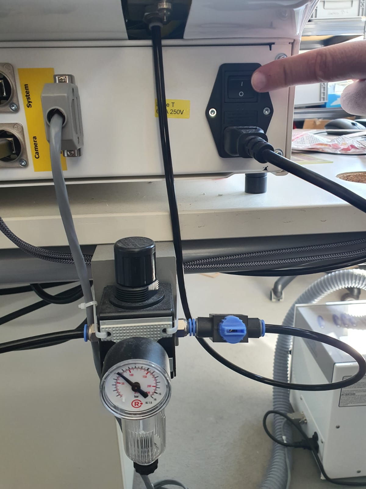
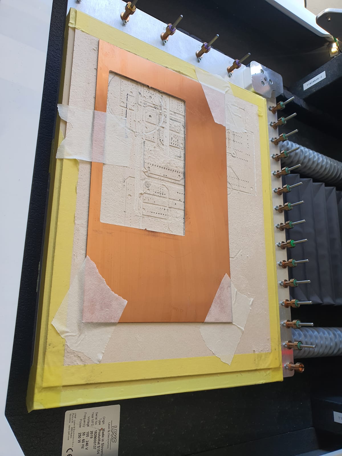
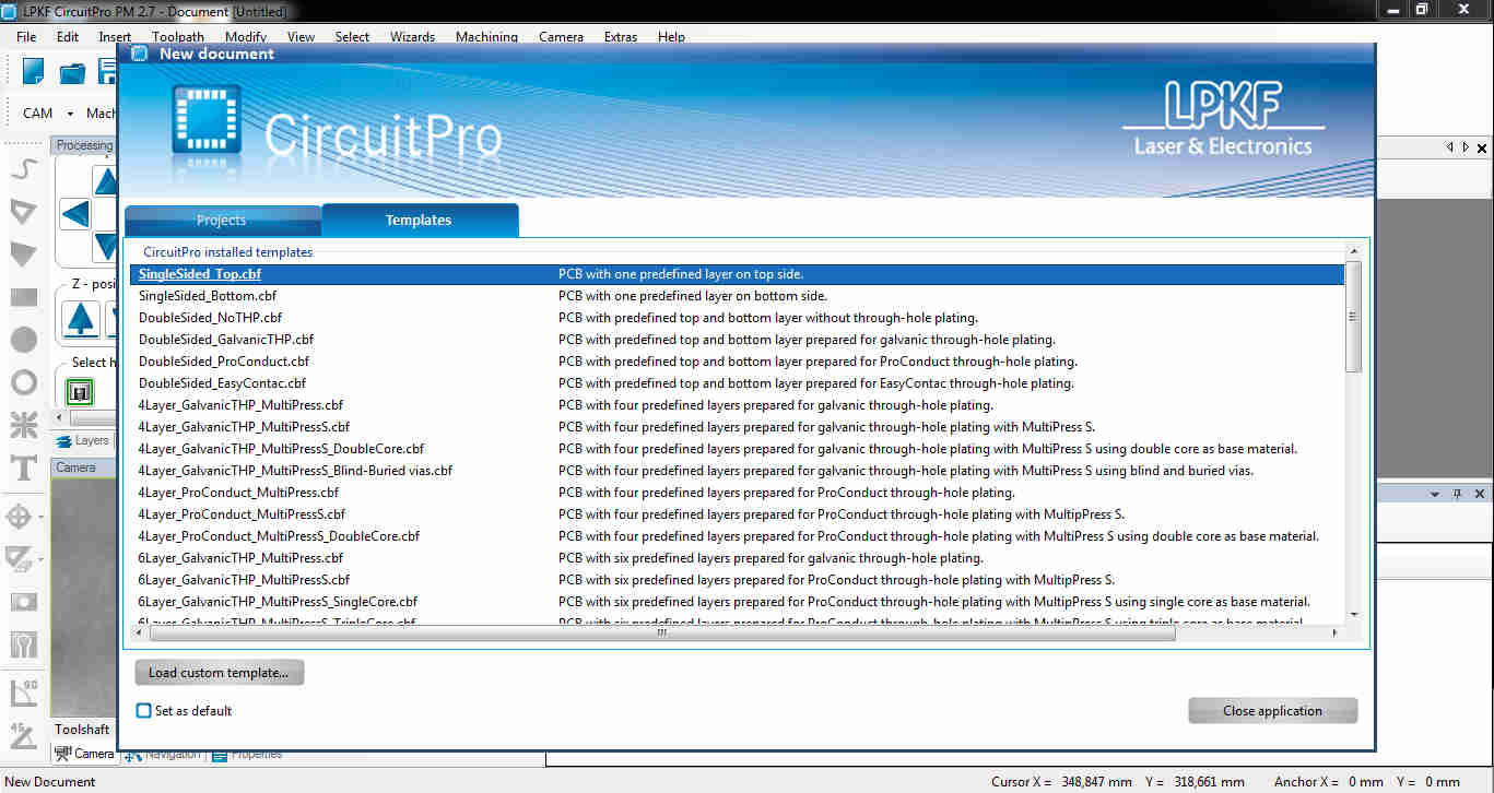
To start the machine, first open the compressed air (~5-6 bar of pressure) and turn on the main switch on the back of the machine. Followed by starting CircuitPro. The Machine will then go through a Startup process including homing for referencing. Also the the programm asked what project should be opened. We used the standard template
Now, you can place the copper material on the bed and use paper tape to keep it in place. It also has a vacuum table but the tape prevent the material from moving bevor and after the vacuum is on.
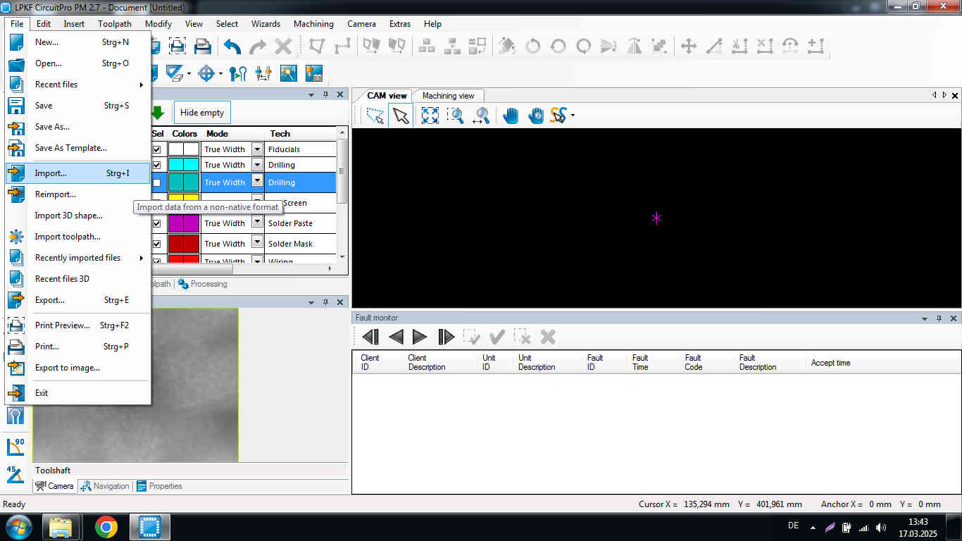
Importing Gerberfiles
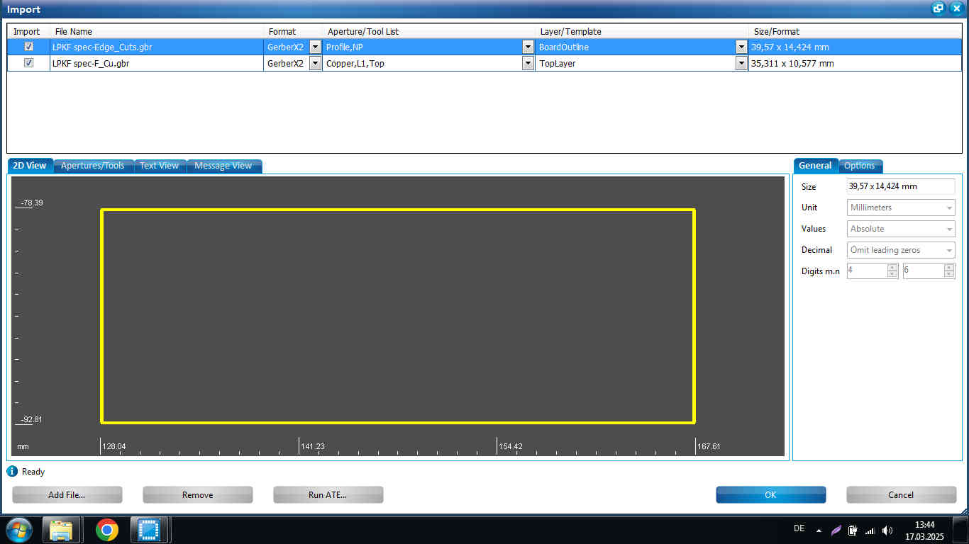
- import Gerber files (cut edges and F.Cu)
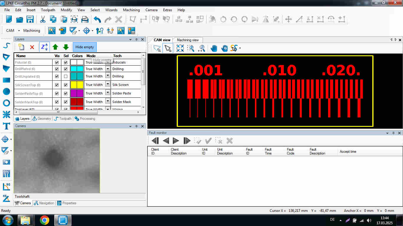
- Always check “hide empty” to
- Mode: Machine tries to capture the True Width of the PCB
- Tech: Wiring means traces, which is based mechanical cutting all the way through the copper layer.
- Phase: milling top → control routing: cutting it out
Trace Generation Settings
- To generate the traces, set parameters:
- Material Type: FR4 (Possible packing material: cupboard, fiber glass, aluminum when you want to dissipate heat, ..etc)
- Cu thickness: 35 μm
- Process: There are four options:
- 4/4: full rub out → all material gets removed or “rubbed off”
- ¾ partial rub out: focus on the traces close together where you need to solder
- ¼ basic: very small isolation lines
- We selected option ¼ basic and modified further settings.
- Available tools: Universal Cutter 0.2 mm (tip is 0.2 and the thickest is 0.5mm)
- Isolation Width: 0.45 mm (how far is the distance between the traces)
- Pads isolation: 0.45 mm
- Channels: determines how many times you want to mill over the material. Set it to 3.
- Rubout: Concentric (in circular)
Contour Routing Settings
-
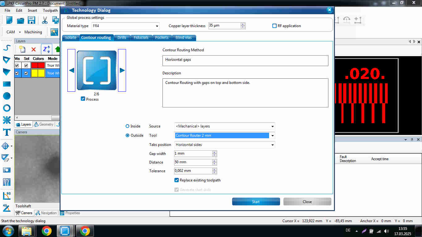
- Contour Routing tab
- Process: select 2/6 tab to fix the cutout PCB into the material so it does not fly or shift during the milling process
- Tool width: 2 mm
- Pockets is when you want something to sit deeper onto the PCB or pass a cable
- Contour Routing tab
Drill Settings
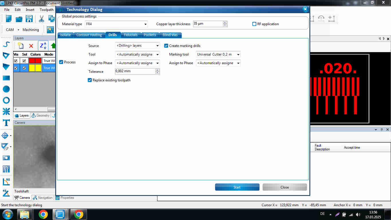
Check on create marking drills; this helps guide the drill to be perpendicular onto the material
Board Production Process
- Start the board production wizard
- Material Settings window pops
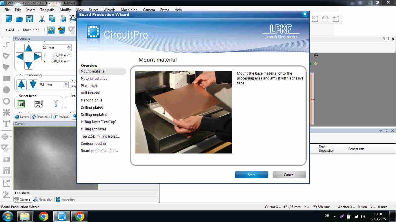
- Material Thickness: 1.5 mm
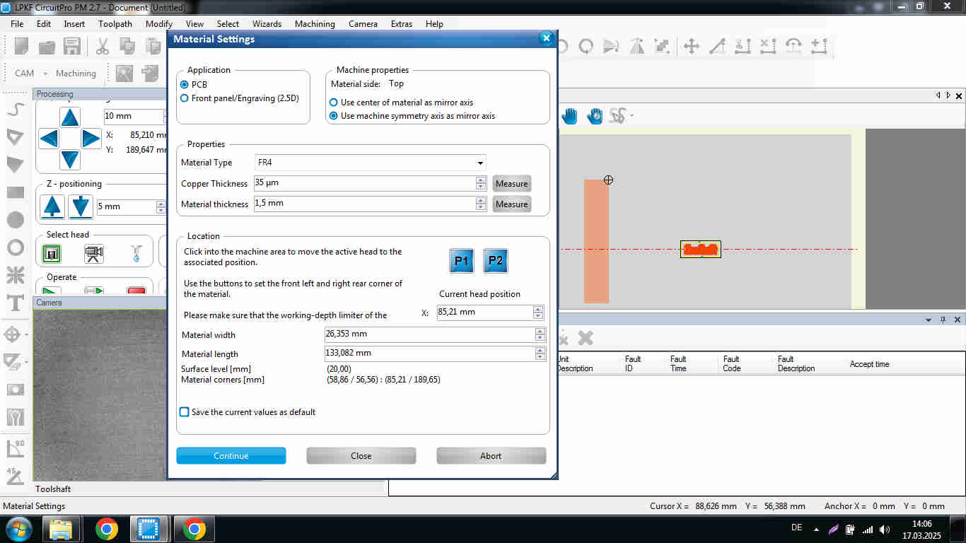
- Board location: specifying P1 and P2
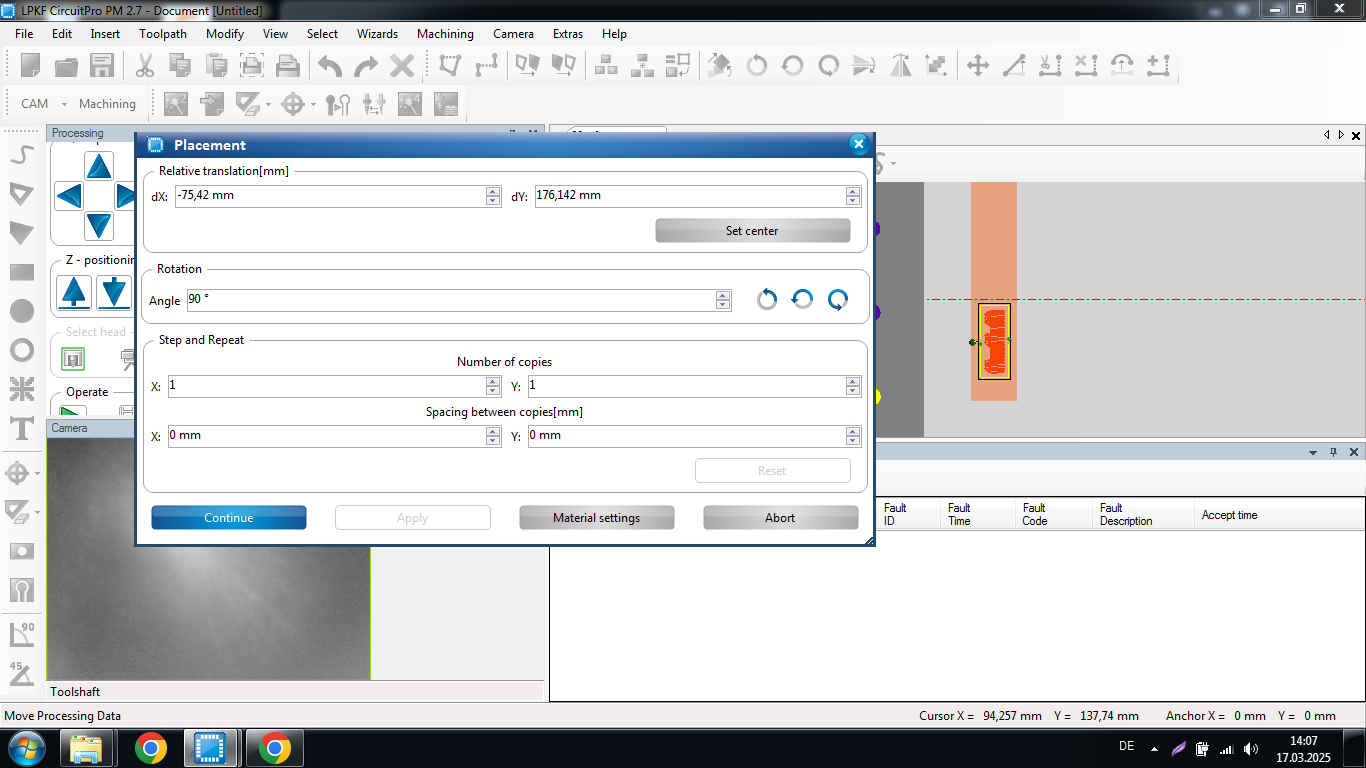
- Placement window pops and alright you PCB into the desired location on the material
- It will prompt you to select the area where to make a test for the depth (z dimension) (since the tip is V-bit, it can easily automate the zero point and it adjust according the head accordingly)
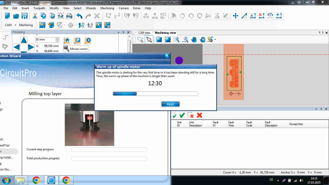
- Since the machine is a professional high end machine and it has not been used for quite some time, it took about 17 min to warm up the spindle motor.
- Finally, the milling and cutting of PCB start and it is just a waiting game.
Characterization
The LPKF uses gerber files that our instructor provided. After milling the traces as already described, we acquired a very precise milling. No trace failed. The LPFK was able to mill out clearances as small as 0.02mm. This demonstrates a highly precise machining and automated processing of the LPKF.
In conclusion, LPKF is a smart machine; it can automatically calibrate the Z-axis and change the tools. Although the smallest clearance was incomplete, indicating the necessity for repeated passes or an other tool, it cut the majority of widths and clearances cleanly.
Final Result
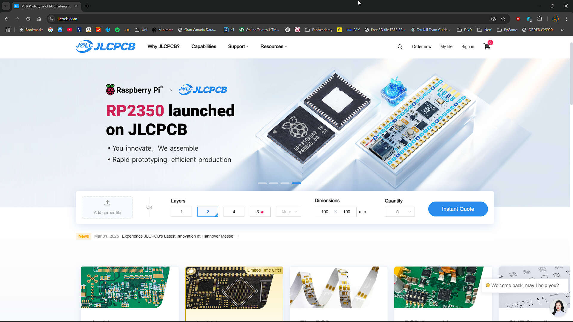
JLCPCB
The second Assignment was to send a board to an Boardhouse. We now simulated the process or show how we would do it. Our problem is, that we are bound to the restrictions of ordering like a university in Germany. We are not allowed to directly oreder from China and German manufacturas are realy expensiv.
Gerber-files
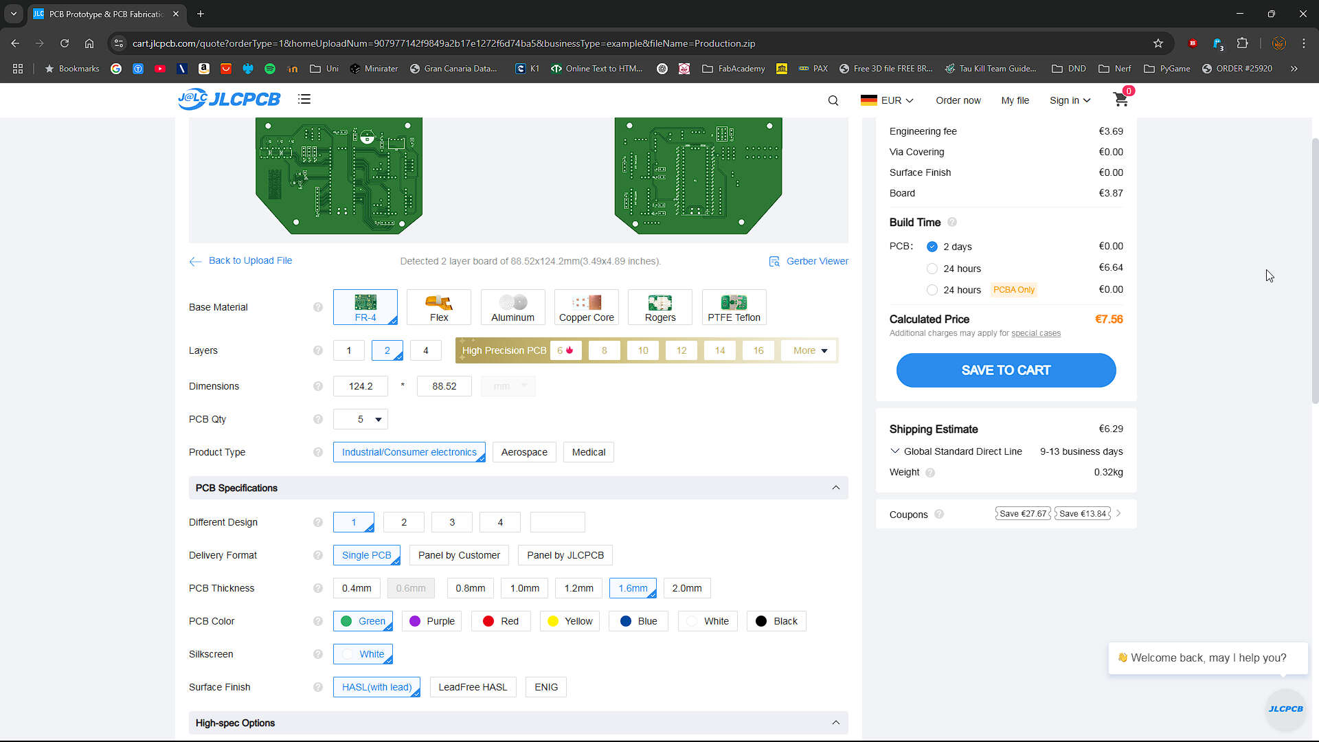
With the Gerber and Drill-files zipped, we uploaded these files to JLCPCB.
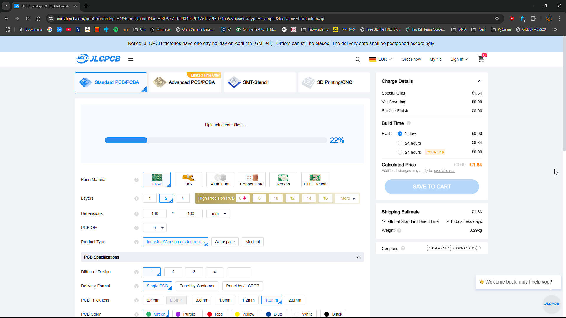
Settings
Base Specifications
- Base Material: FR4
- The standard Material to order, the rest is too expensive and too excessive for most applications.
- Dimensions: auto
- JLCPCB gets the dimensions from the gerber files
- PCB Qt: 5
- Standard and smallest amount.
- Producttype: industrial/Consumer
- Describes the Quality which is required
PCB Specifications
- Different Design: 1
- amount of different Boards in your Files
- Delivery Format: Single PCB
- Already cut. Panel means that the pcbs are nested and connected to each other. Normally used with a pick and place machine
- PCB Thickness: 1.6mm
- Standard. thickness Depends on your Requirements. Higher Thickness means more stability
- PCB Color: green
- Color of the Solder Mask. Switching Color is just for the appearance
- Silkscreen: White
- The Color all the marks and writings on your Silkscreen layer
- Surface finish : LeadFree HASL
- Pre-tinned Pads. Go with LeadFree to prevent lead vapour while soldering. ENIG means Gold plated.
High-Specs Options
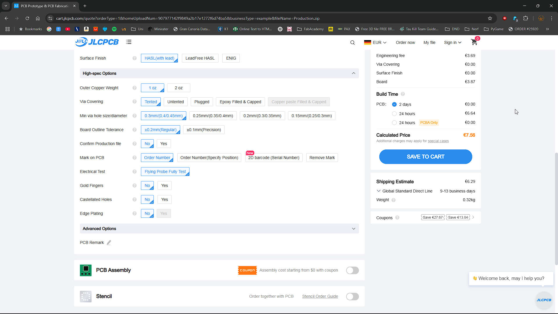
- Outer Copper Weight: 1 oz
- Standard. More means we can use higher power
- Via Covering: Tented
- Tented means covered. Untented means that the Soldermask was removed to expose the vias and their pads
- Min via hole size/diameter: 0.3mm(0.4/0.45mm)
- That means, that in our design, the holes of the via needed to be at least 0.3mm large and the vias itself 0.4/0.45mm
- Board Outline Tolerance : +-0.2mm
- Standard. That means that our Board can be smaller or larger within the tolerances.
- Confirm Production Files : No
- If you say yes, then the Production files will be sent to you and you have 48h to review them and confirm them or to add changes.
- Mark on PCB: Order Number
- JLCPCB will add the Order Number on the Silkscreen somewhere on the Board
- Electrical Test: Flying Probe Fully Test.
- The only option for 2 Layer PCB. It tests if the Vias for example are working.
- Gold Fingers: NO
- If you want to plug your Board for example in an USB Port or you are making your own PCI-E Cards or RAM Sticks
- Castellated Holes: No
- These Holes are Half and the edge of a board for soldering the board to another board. See the PI Pico as Example.
- Edge Plating: No
- Plating the edges to Prevent for example the exposure of the Fibers of the Board Material to the air and preventing fibers infusing the air.
