Microcontroller development board
- Measure something: add a sensor to a microcontroller board that you have designed and read it
Some circuit boards is designed in Fusion360 in the week 6 assignment, and I will try to make them as the assignment development board. In the week 6 assignment, after the design is completed, I export the file in grb format(for top copper layer and profile) and xln format (for drill)
Making the development board
The next step is finding a way to manufacture the development board. The machine I can find to make the development board in the FABLAB Macao Science Center is CNC milling machine.
In the week 7 assignment, I'd learnt and tried to use the CNC machine, and this time the same technology can be used to make the development board with single-sided PCB board.
Single-sided PCB board is a type of board basically make with glass fiber(insulation material), and has a thin copper layer on only one side of board(conductive material). We can make the development board by milling the extra part of the thin copper layer, and let the remind copper to form the circuit.
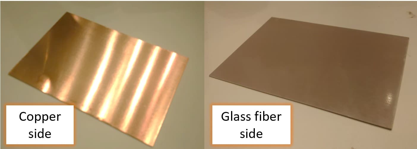 A raw single-sided PCB board
Before the process started, we need to know the format of the machine needed. The model of the machine in our LAB is MDX-50, by the instructions from the FABLAB BRIGHTON 2018, the format it need is RML.
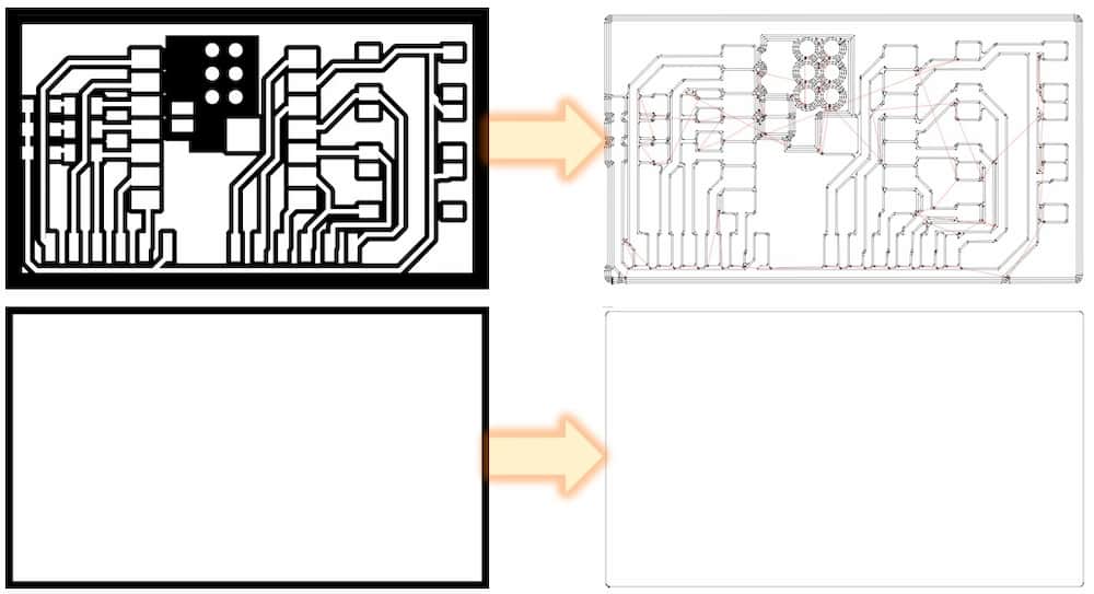
Generating the CNC file
The instruction provide a online converter, fabmodules.org (current is https://modsproject.org/) to generate a rml file from png file, and there is also some online converter can convert the grb and xln file to png file.
So in summary, the convert process can be divided into 2 steps:
- Convert the
.grbfile topngfile - Convert the
pngfile tormlfile
grb/xln to png
The online converter is https://gerber2png.fablabkerala.in/
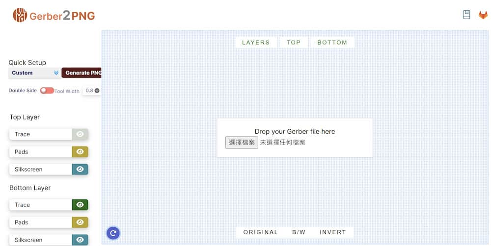
grb/xln file into the center part, and it will convert the file to a picture form.
::: info
If it doesn't generate the picture automatically, just refresh the page and drag the file again.
:::
Here I will use the THT component version top copper.grb file in week 6 assignment as a input example, the result will be like these:
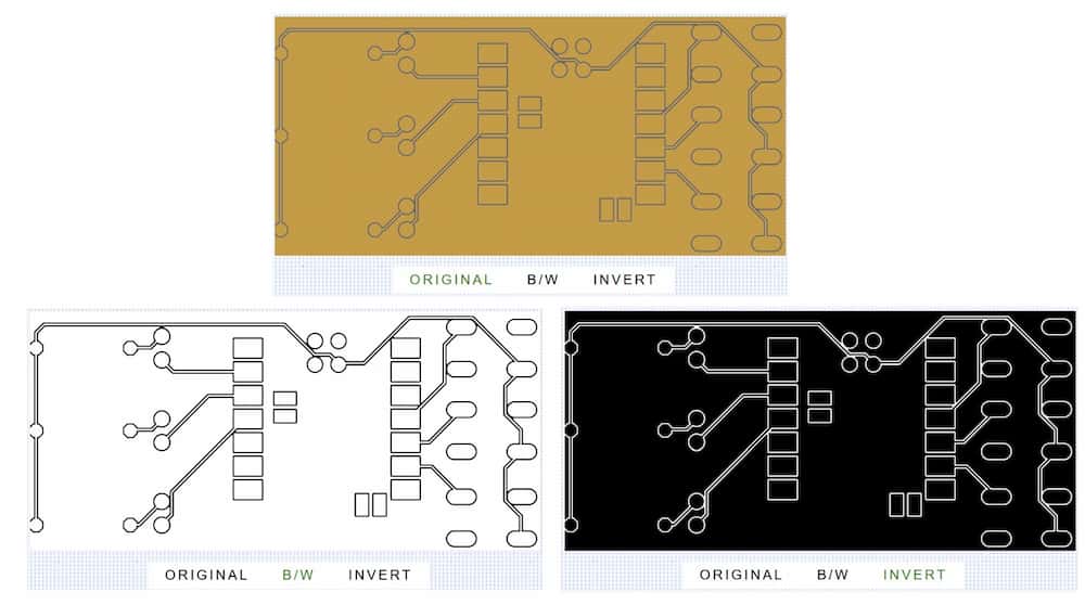
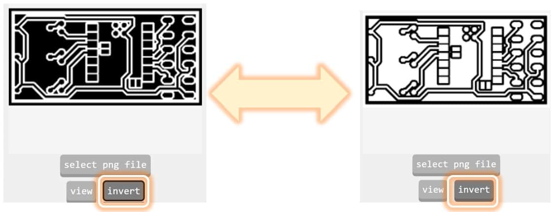
ORIGINAL, B/W and INVERT, and all we need is the B/W one for the next step.
If you choose the INVERT one, it can still be inverted back to the B/W effect in the next step.
To make some more space at the outline, I drag both the top copper.grb and the profile.grb file in the same time to form a better outline result.
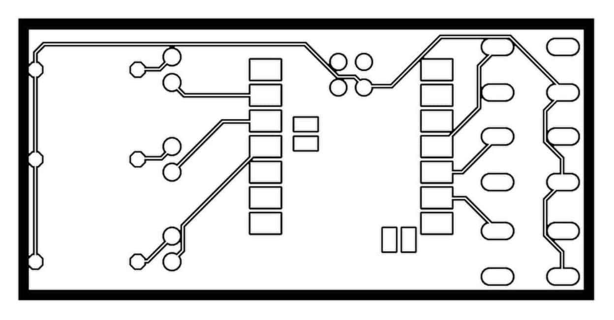
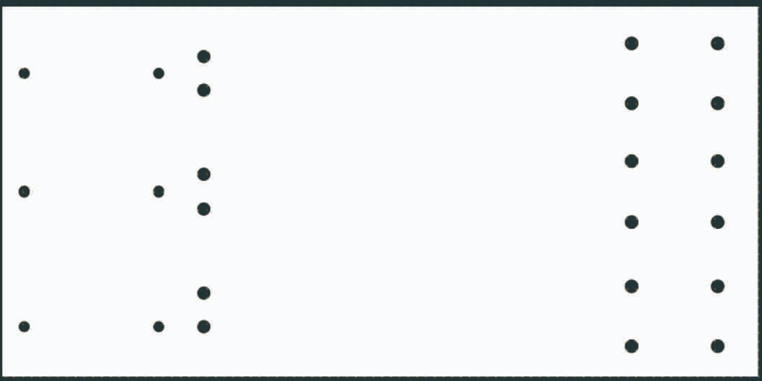
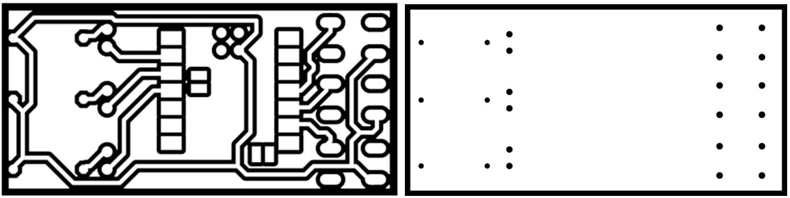
The above one is for the milling process (to form the circuit), and we also need to do another png file for the cutting and drilling process (to drill the hole and cut the board from the raw material).
I drag both the drill.xln and the profile.grb file in this time.
Avoiding the copper width being too thin for the milling process, I also generate a wider path version by adjust the design rule in Fusion360, To classify the difference version, the thinner one will name as THT v1 and the wider one will name as THT v2.
The copper width route and clearance is both set as 6 mil in THT v1 and both of them is set as 24mil in THT v2.
 The two png of THT v2
And also I generate the SMT component version
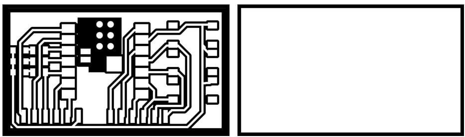 The two png of SMT version
png to rml
After generate the png file, the next step is convert them into rml file.
The old link(fabmodules.org) is no longer available, and the new converter is https://modsproject.org/.
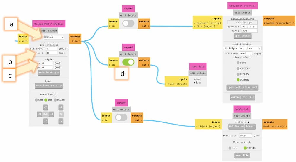
By right click to start, choose program - open program - Roland-MDX - mill-PCB, then we will enter the interface like this:
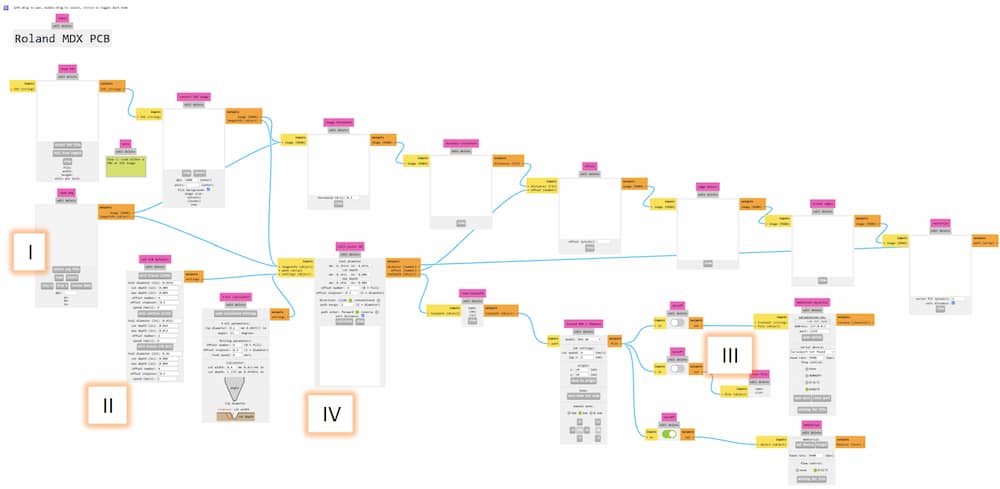
- I. First import the
pngfile here. - II. Select the tool for mill trace / outline.
Details
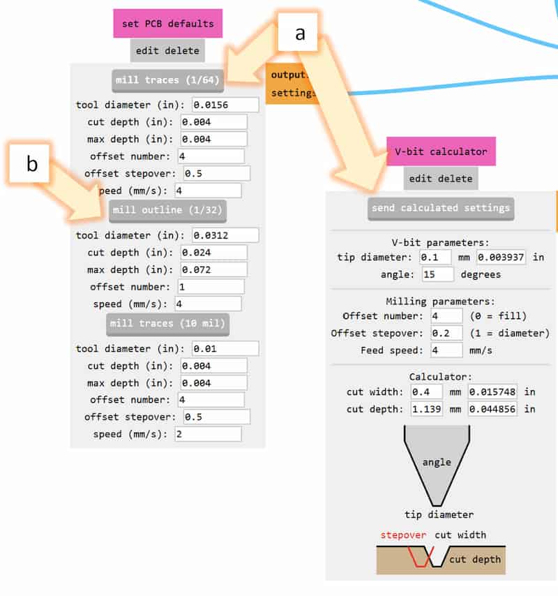
(b) For outline milling (cut through or drill through), we will use a mill tool with bigger diameter. (Default as 1/32in, or 0.8mm)
If the tool you used isn't the same size as the default one, you can change the parameter by yourself.
- III. Set the output detail.
Details
(b) The
jog z mean the Z-axis starting point. It shouldn't be too low, as the tool would crush if there are any bulge object.(c) Here to set the X,Y-axis starting point from the 0,0 point. If you set the orginal point perfectly, you can just set it both 0mm, so it will start just at the orignal point you set.
(d) Choose the output method to the CNC machine. If your computer is connect directly to the CNC machine or connect with network, you can choose the top one or bottom one to send your
rml file, but in my case, my computer doesn't connect to the CNC machine, so I choose the middle one to generate the file to the loacl drive, and transfer the file by USB to the CNC computer later.- IV. calcualate and download the file
Details
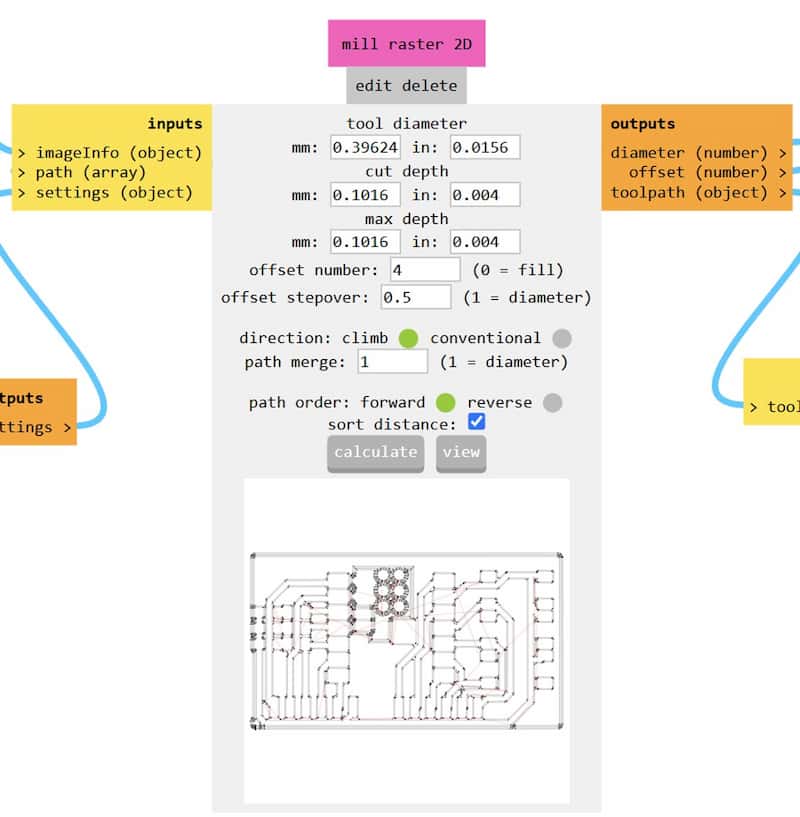
(b) Click the
calculate button to calculate the path. Also it will start download the rml file.(c) Although the file is downloaded, don't forget to confirm the process diagram below, and you can click the
view button to see it more clear.
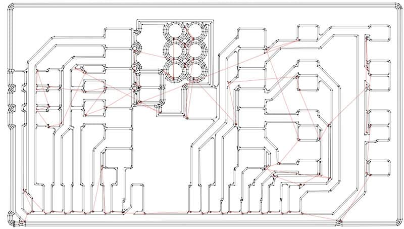
Check the milling path
Result of the THT v1:
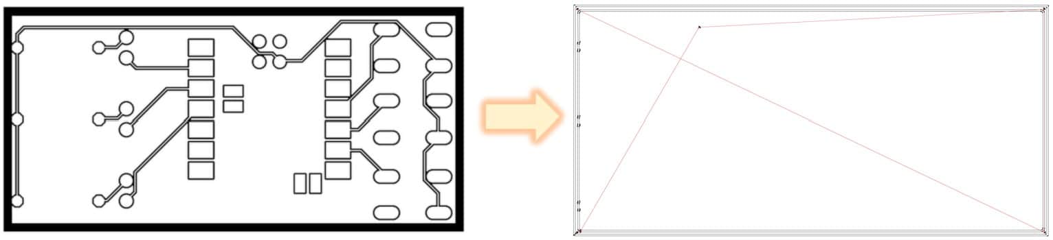
The path and clearance is too thin for the convert to generate the milling path. So the THT v1 design is failed.
Result of the THT v2:
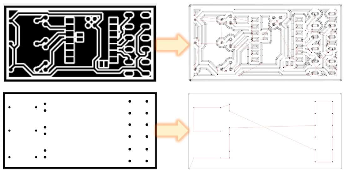
As the convert is assume to mill the black color parts, if you generate a invert png in the last step, the milling path will be also invert and will mill all circult parts!
invert button after the invert png is loaded, and convert it back to the normal one.
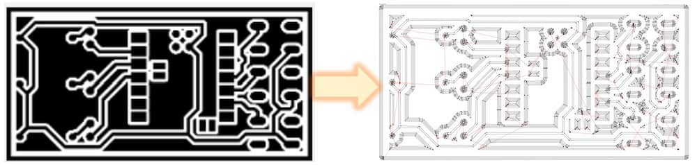
Result of the SMD:
Pre-processing on the machine
Here is the MDX-50 CNC machine, and there is some important parts we need to know about the machine:
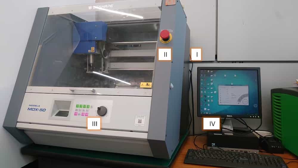
Details
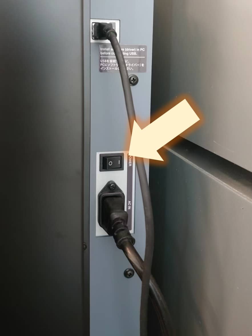
I. The power switch
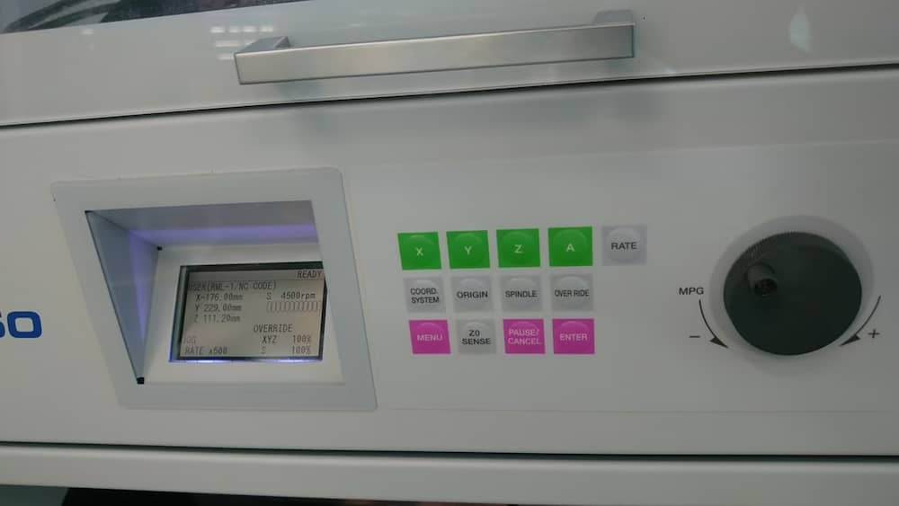
For more specifications, check the offical website
Install / Change the milling tool
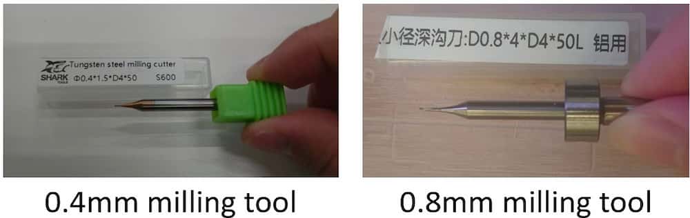
First we need to install the tool to the machine. The tool we used is same as the one we set in last part: 0.4mm (1/64 in) milling tool and 0.8mm (1/32 in) milling tool.
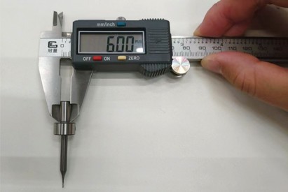
The machine is compatible to the tool handle with 6mm diameter, so if the tool handle we prepared isn't fit, we need to install it to a 6mm converter.
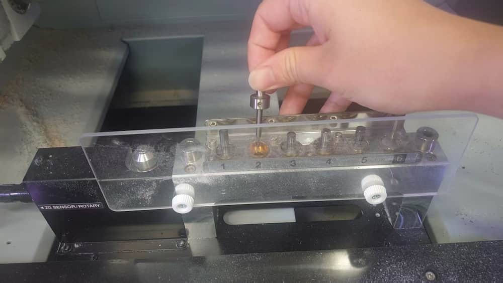
Tool 6 in the tool station is used for the calibration for the rotation axis, which can't be replace with other custom tool.
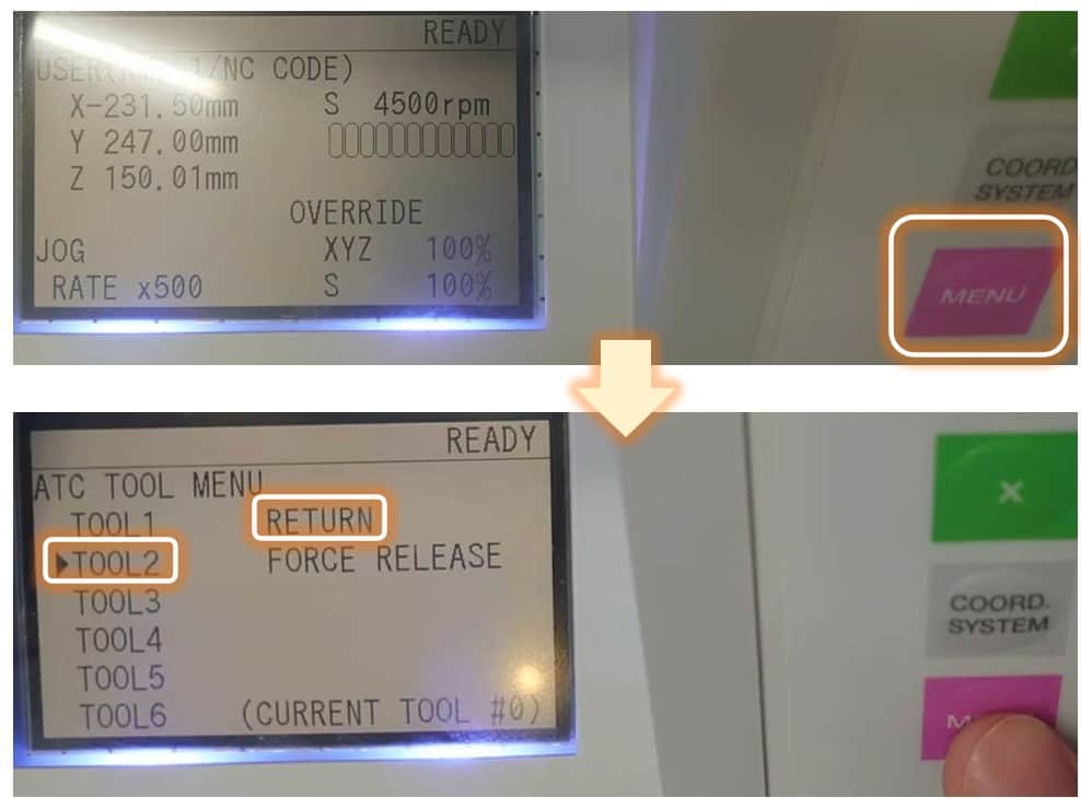
Press the MENU button twice to go to the tool choosing interface, and choose TOOL 2. The machine will install the tool 2 and calibrate the height automatically. To release the current tool back to the tool station, press the RETURN.
Install the PCB board
The PCB can be fixed on the platform by double sided tape. Make sure the copper facing up!

Set Z orginal point
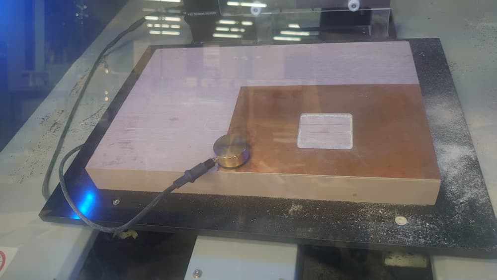
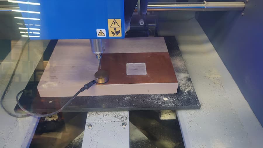
After the tool and the PCB board is installed, we need to set the orginal point of the Z axis. There is a Z0 sensor connect to the machine, and we need to place the sensor to the surface of the PCB board.
X,Y, Z buttons and the rotary knob to adjust the tool until it is right above the sensor
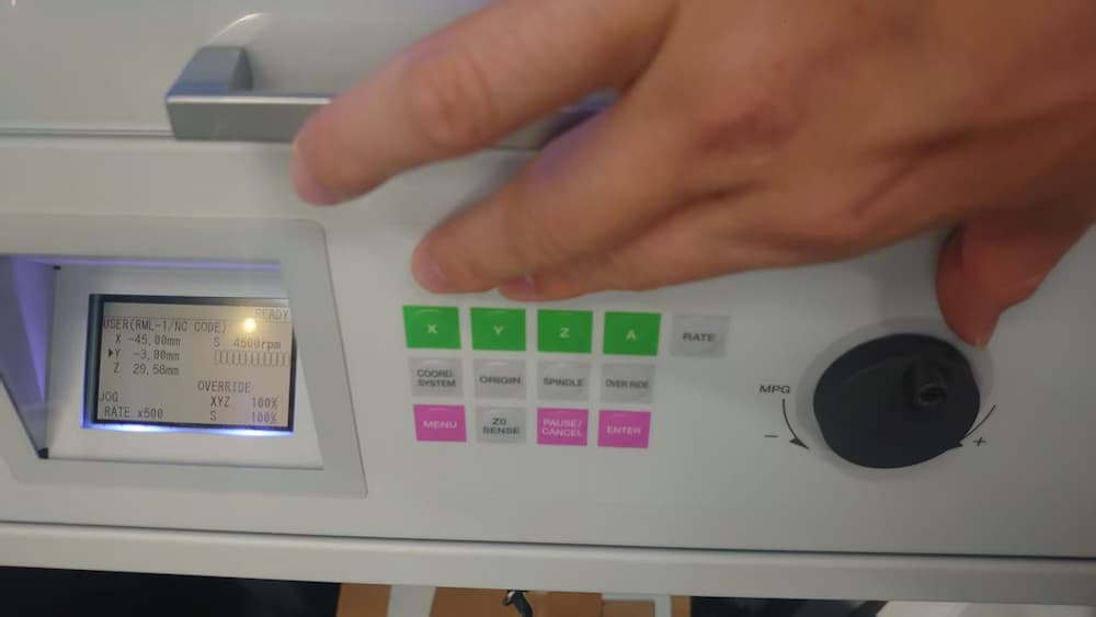
Z0 sensor button to let the machine do the Z orginal point calibration.
After the next step, the milling process will start, and we possibly won't touch the machine again after this step, so make sure the following point is checked and complete!
- When you open the cover, the tool end will drop a little bit downward, make sure DON'T open the cover when there's something under and close to the tool end!
- After the Z orginal process is finished, DON'T forget to remove the sensor from the PCB board!
- Clear the platform, confirm there AREN'T any obstruction on the platform.
- The tool will move through the X and Y axis first, and finally the Z axis. Make sure the till end is raised HIGH enough before start!
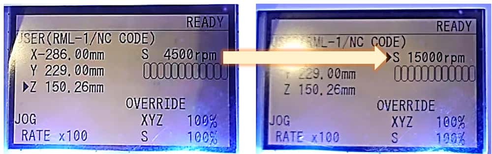
- The spindle's default setting is 4500 rpm, and here is almost the final chance to set it back to the max speed 15000 rpm!
Control software
Back to the control computer, the controlling software is VPanel for MDX-50

settings button to set the XY orginal point and click the cut button to read the rml files.
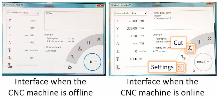
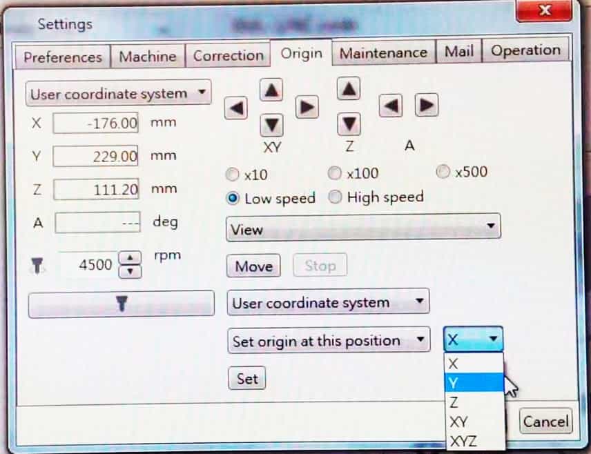
Set X-Y orginal point
In the settings interface, we can set the X,Y orginal point in the orgin tab.
Start Milling
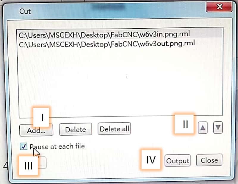
cut interface, we can:I. Add the
rml file to the softwareII. Use the arrow to adjust the order of the file to mill. Remember to mill the copper circult first, and final cut the board.
III. If you add both file in, we must tick the pause to make it stop at the first mill, give us time to change the milling tool for the final mill.
IV. After press the output, the milling process will start immediately! Rememeber to keep the platform clear and the milling tool in a suitable place so it won't be crushed.
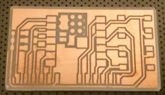
With the limit time, I only mill the SMT version. The first milling process for the top copper layer
And the final result:
Complete the board
After the milling process is finished, the most difficult part is finished.
Test with the multimeter
Before install the component, we have to check if there are some copper haven't be mill. I use the multimeter to check if the conductivity of the circult is OK.

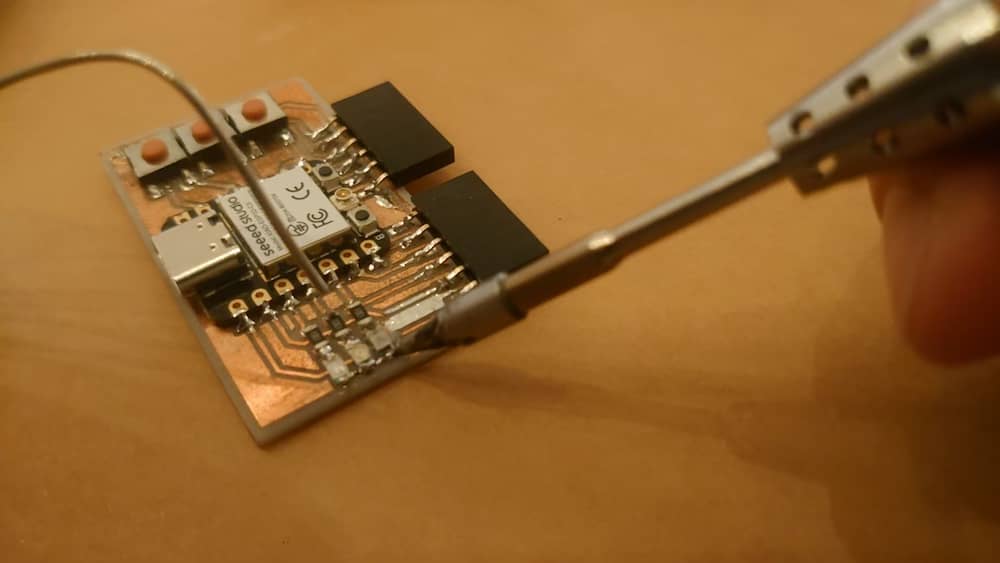
Soldering
Here are the tool needed:
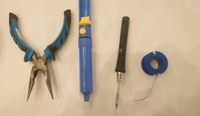
Solder sucker - remove the extra solder wire
Solder - heat and melt the solder wire
Solder wire - connecting the electric component
The soldering order should be start from the inner components to the outer components.
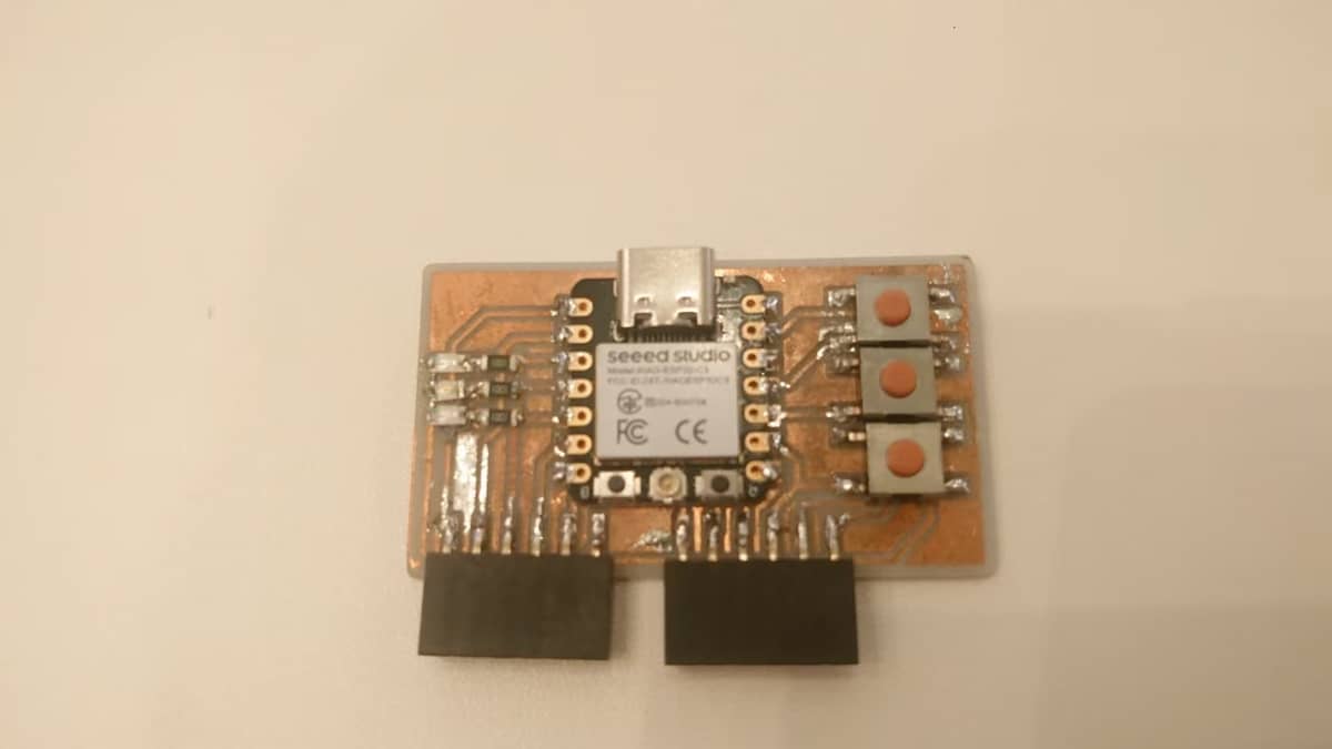
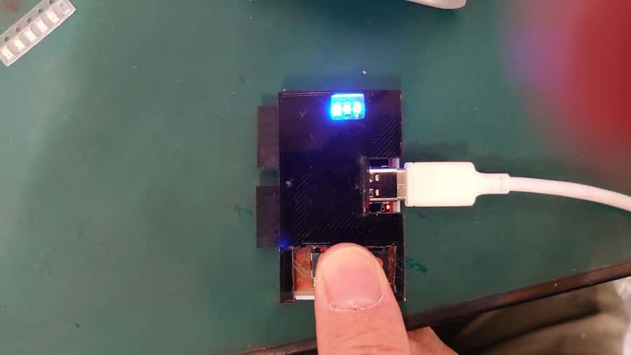
The final testing
The test program is the one in week 4 assignment, using one button to control one LED.
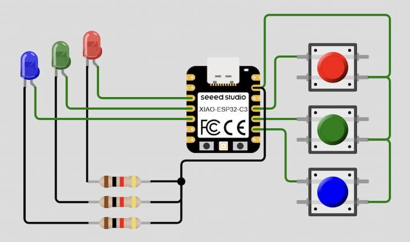
Programming detail
void setup() {
  Serial.begin(115200);
  pinMode(D2, OUTPUT);
  pinMode(D3, OUTPUT);
  pinMode(D4, OUTPUT);
  pinMode(D10, INPUT_PULLUP); //set as INPUT_PULLUP, which mean active the pullup resistor inside the microcontroller, avoiding the short circuit when the button is pressed.
  pinMode(D9, INPUT_PULLUP);  //when pin is set as pull up, the digital read result will always be 1
  pinMode(D8, INPUT_PULLUP);  //and only become 0 when the button is pressed.
}

void loop() {
  if (digitalRead(D10)==0){digitalWrite(D2, HIGH);} //
  else { digitalWrite(D2, LOW);}

  if (digitalRead(D9)==0){digitalWrite(D3, HIGH);}
  else { digitalWrite(D3, LOW);}

  if (digitalRead(D8)==0){digitalWrite(D4, HIGH);}
  else { digitalWrite(D4, LOW);}
}
Simulation:
Here is the final result:
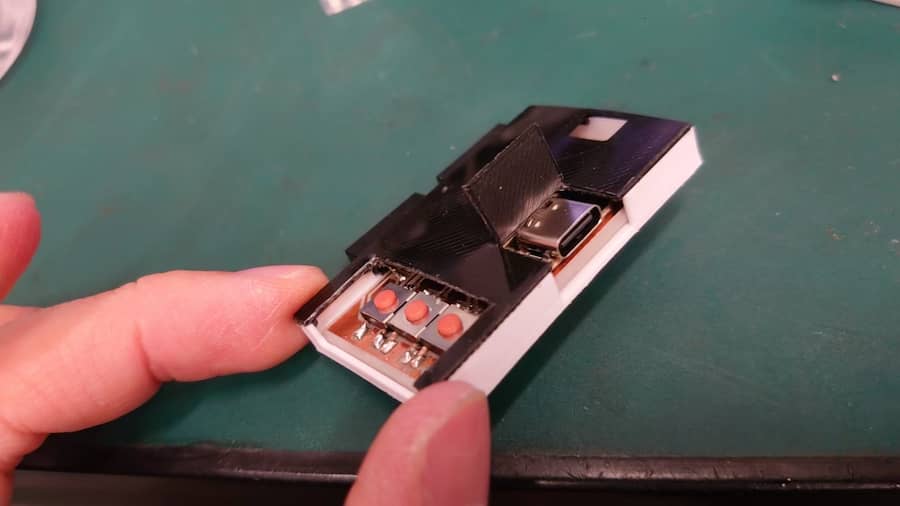
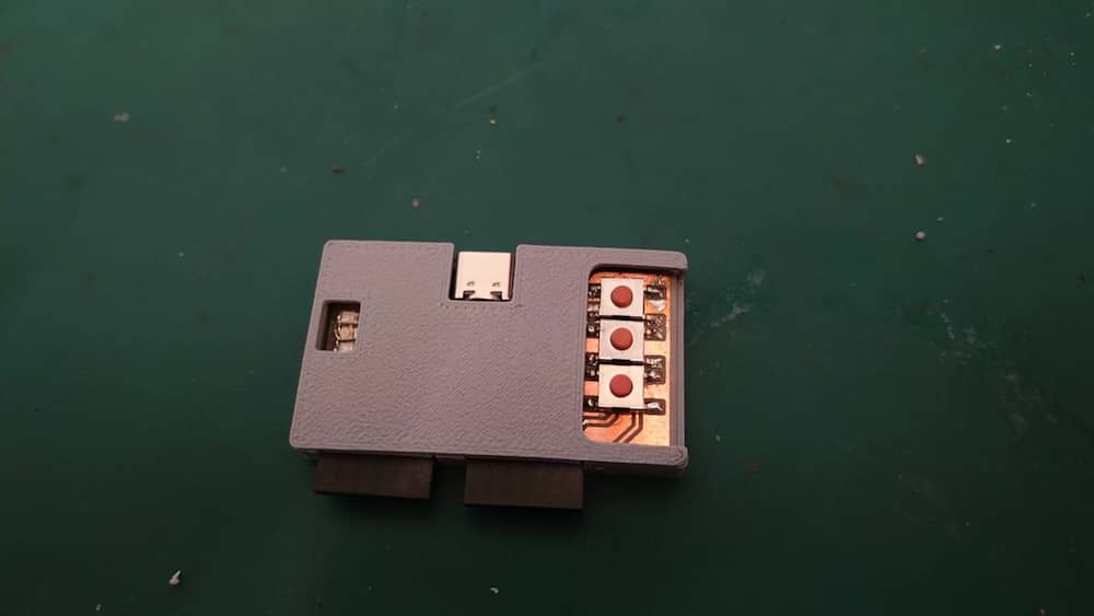
Extra case
In the week6 assignment, I also design a case base on the PCB board as a protection, so I print it out and connect to the board.