EDA design
- Use an EDA tool to design a development board that uses parts from the inventory to interact and communicate with an embedded microcontroller
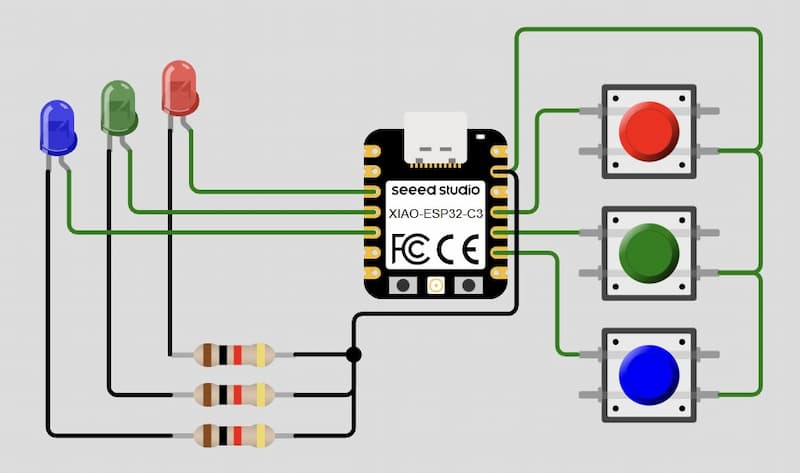
The circuit designed in week 4 assignment match the target of this week, so I will work on the further design base on this circuit design.
Programming detail
void setup() {
  Serial.begin(115200);
  pinMode(D2, OUTPUT);
  pinMode(D3, OUTPUT);
  pinMode(D4, OUTPUT);
  pinMode(D10, INPUT_PULLUP); //set as INPUT_PULLUP, which mean active the pullup resistor inside the microcontroller, avoiding the short circuit when the button is pressed.
  pinMode(D9, INPUT_PULLUP);  //when pin is set as pull up, the digital read result will always be 1
  pinMode(D8, INPUT_PULLUP);  //and only become 0 when the button is pressed.
}

void loop() {
  if (digitalRead(D10)==0){digitalWrite(D2, HIGH);} //
  else { digitalWrite(D2, LOW);}

  if (digitalRead(D9)==0){digitalWrite(D3, HIGH);}
  else { digitalWrite(D3, LOW);}

  if (digitalRead(D8)==0){digitalWrite(D4, HIGH);}
  else { digitalWrite(D4, LOW);}
}
Result: https://wokwi.com/projects/424317095939542017
EDA tool - Fusino 360
Fusion 360 not only be used for 3D modeling, but also can be a EDA tool for electronic design. We can choose New Electronics Design from the File icon to start the new design.

SHEETS page.
1. Build the circult
In this step, we need to decide the components we need, and connect them as a circuit.
Process to build the circuit
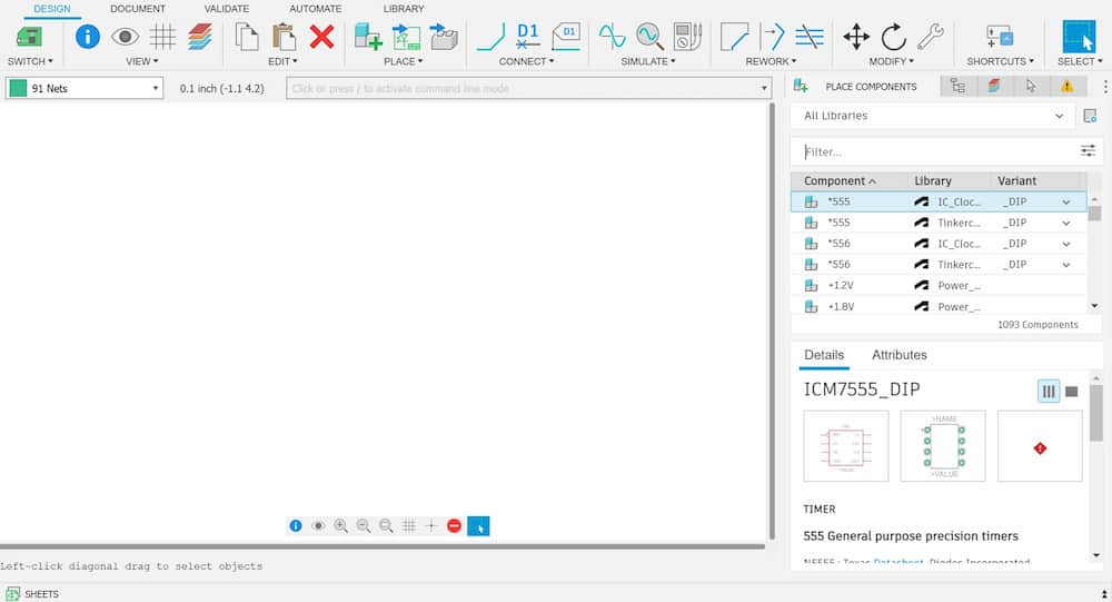
We can search component we need in the right PLACE COMPONENTS bar.
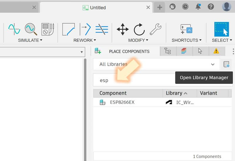
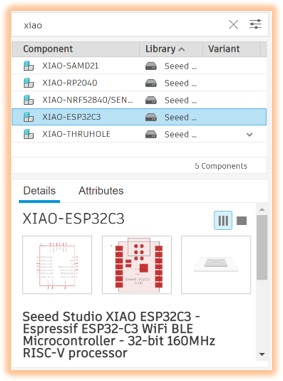
esp32, which means it is not in the default component in the component list.Install the library
So we need install the exact component library. We can download the XIAO ESP32C3 component through the Open Parts Library: https://github.com/SeeedFusion/OPL_Eagle_Library
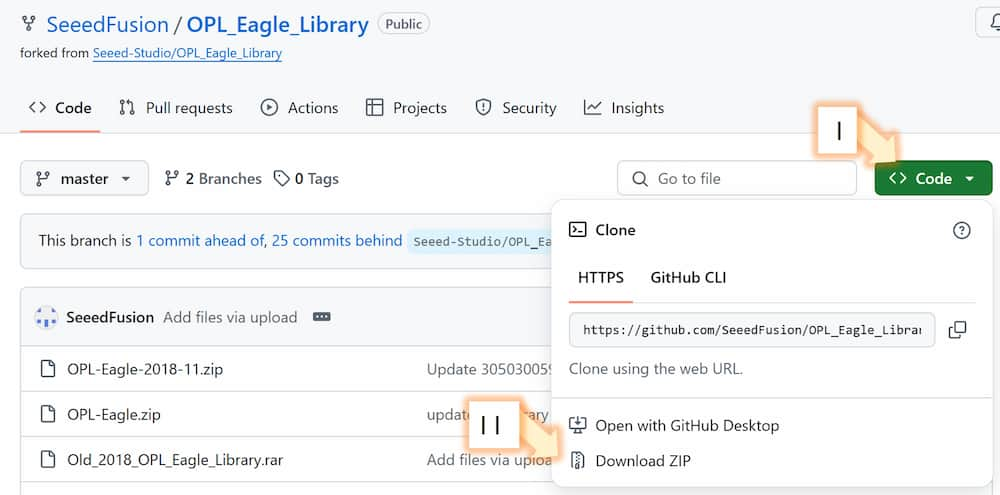
<>Code buttonII. Press
Download ZIP to download the zip files.
I. Click the
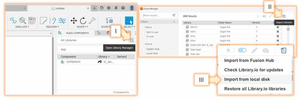
Open Library Manager icon (right)II. Click the
Import libraries iconIII. Click
Import from local disk and choose the .lbr file we download last step. After this step, the library should be installed. We can check again by searching and confirm if we install the library successfully.
NET to connect them.
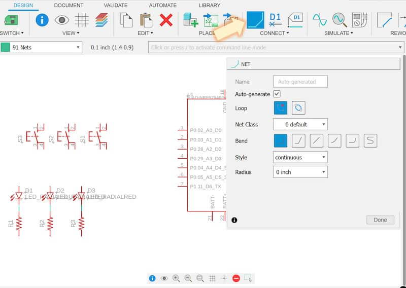
The circuit after connected.
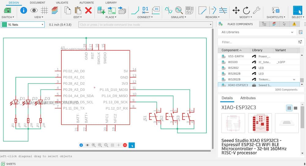
| Component Name | Library | Quantity |
|---|---|---|
| XIAO-ESP32C3 | Seeed Studio XIAO Series | 1 |
| 10-XX | switch-omron | 3 |
| DIP-RES-1K-5%-1/4W(PR-D2.3XL6.5MM) | OPL_Resistor | 3 |
| LED_RADIAL | Opto-Electronic | 3 |
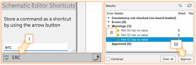
- Electrical Rule Check(ERC)
Always do a Electrical Rule Check(ERC) after the circult is connected, which can help you to find out any potential problems
I. The function can be search with shortkey s.
II. After the checking, the system will show Error or Warning message. Error is something wrong seriously while Warning might not be an error but could cause potential problems.
III. If your Warning message is confirmed not a real problem, you can click the Approve button to cancel the message.
2. Switch to PCB document
After the ERC message is checked, we'll go to the next step, the PCB document section.
Process of building PCB circuit
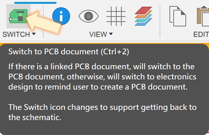
SWITCH icon, the interface will create a new PCB document page. All the component will be change into the real size form in the left bottom corner.
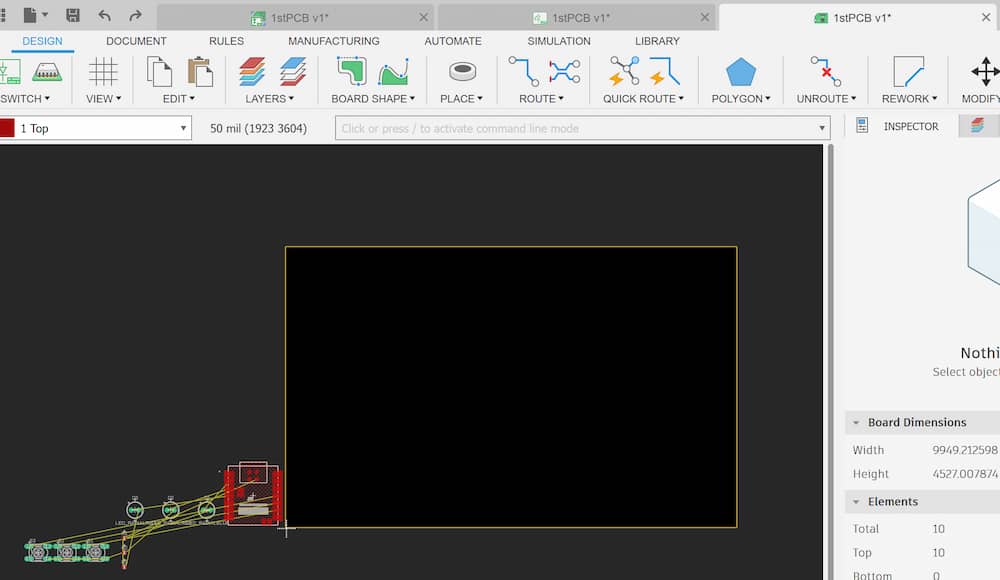
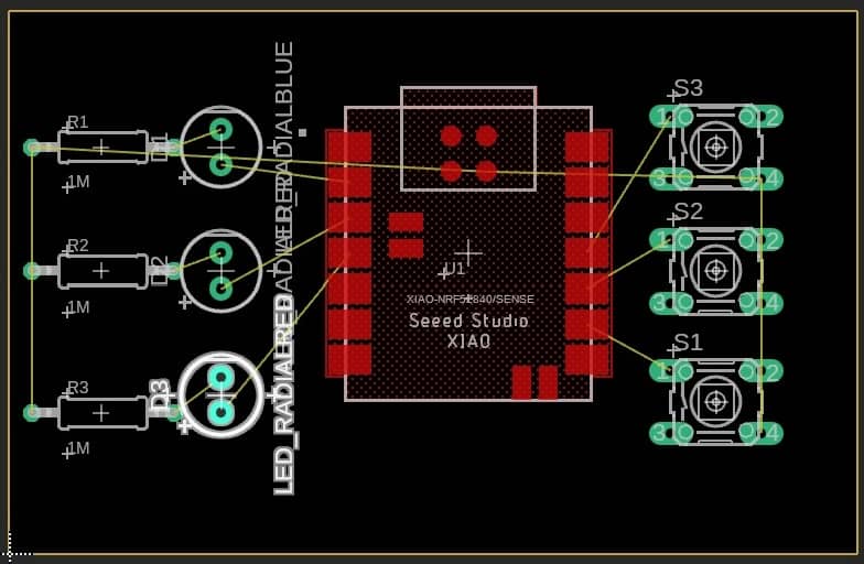
After the arrangement, the circuit should be like:
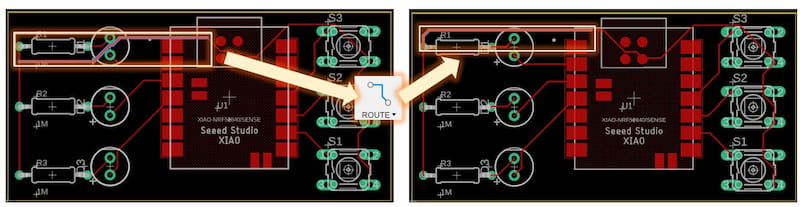
- Route
After the component be arranged, you can see that they are connected with very thin yellow lines, which mean that they are connected, but the actual "road" between them still not build up.
Process of building route
Autorouter
We can use the Autorouter function to buiild the route automatically.
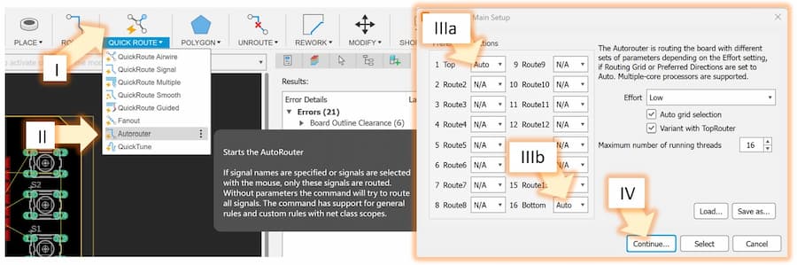
Go to
QUICK ROUTE( I ) icon and click Autorouter( II ). We can decide how many layer are in the board, maximum to 16 layers.If we want to use for the CNC process in future, we just need the top layer, so just keep the
Top layer( IIIa ) and set Bottom layer to N/A( IIIb ).If everything is OK, click
Continue... to the next step( IV ). A new interface will appear showing you some options of the route.
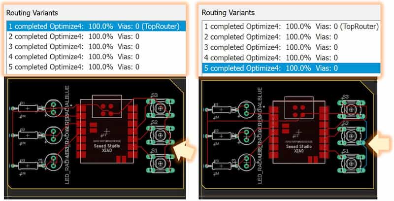
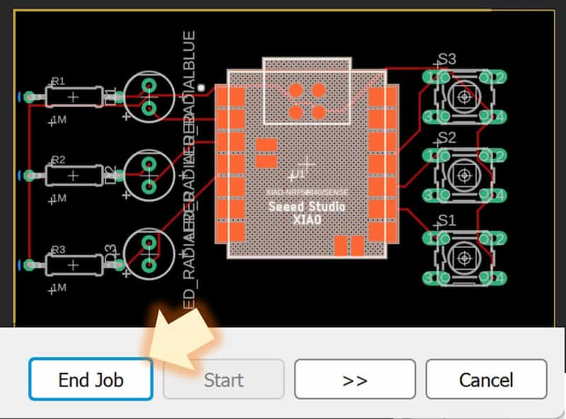
After cofirm the final route, click the
End Job to continue.Manual Route
If some parts of the auto route is still not satisfied, you can delete the route, click the
ROUTE icon and rebuild the route manually.
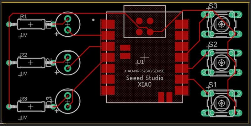
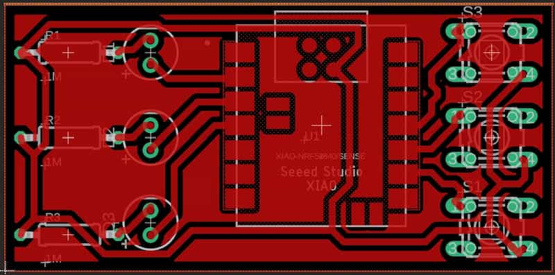
The final result:
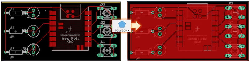
- Polygon
As in the production process, we will cut the thin metal on the top layer, so usually we just need to cut the connecting area beside the routes and the connnection dots. So we have to 'tell' the software which area we need to keep the metal, and it should be as large as it can, to reduce the processing time.
Process of building polygon
Click the Polygon icon to surround the area of the PCB board, and it will fill the emtry place as the metal. Also you can set the metal connect to one of the route, like GND, make it easier for further output connection.
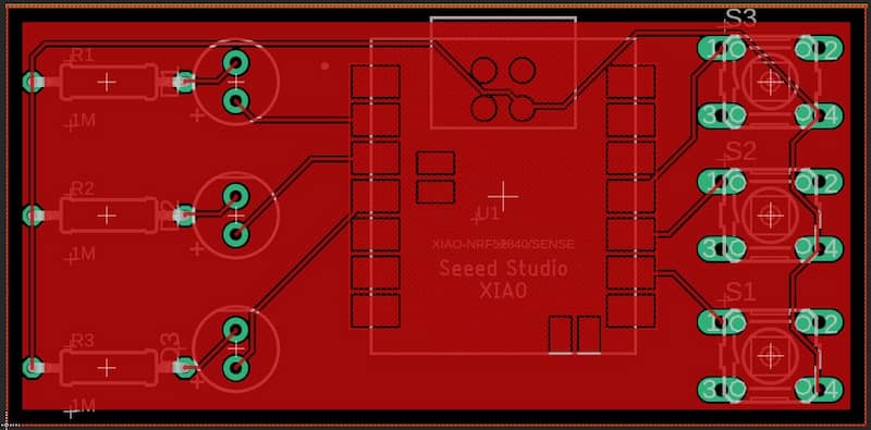
The final result:
- Design Rules (Optional)
If the route and clearance is not satisfied, you can change some parameter in the Design Rules to adjust the size.
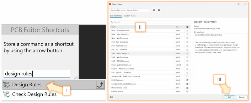
After the parameter is changed, some error might cause, like the metal part be overlaped. So it will be better to delete all routes and regenerate them again.
A sample with a wider copper width route (24 mil) and clearance (24 mil).
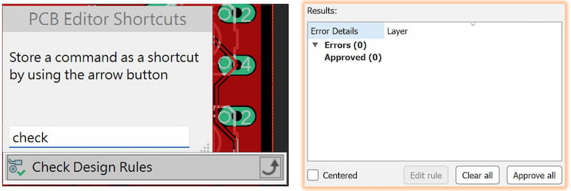
- Check Design Rules
Like Electrical Rule Check(ERC), always do a Check Design Rules after the the circult is finished, which can help you to find out any potential problems.
Basically all processes is same as the Electrical Rule Check(ERC) above, and if there are.
- Export
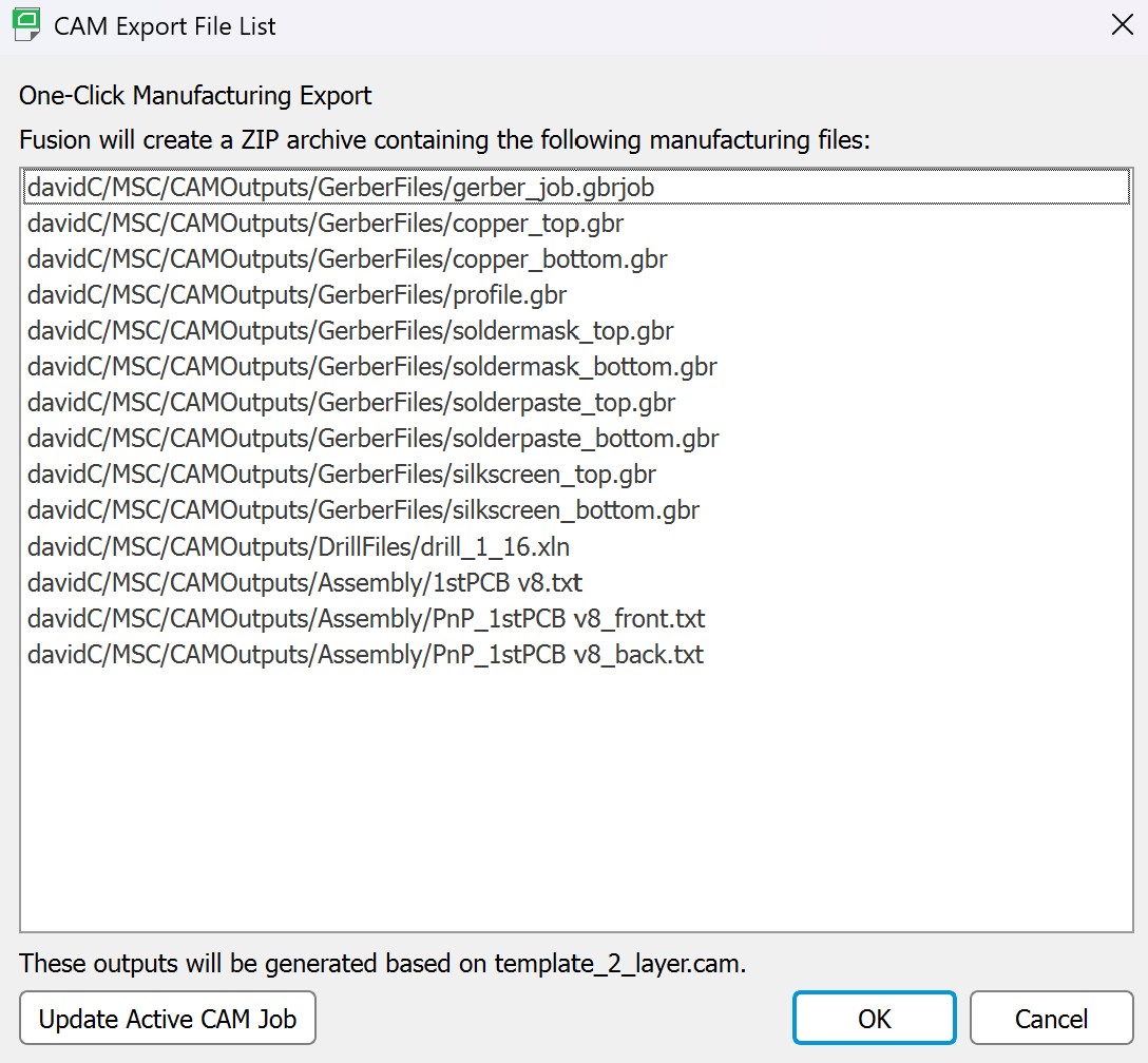
For the further process like CNC milling, we need to export the PCB data from Fusion360 to the CNC machine.
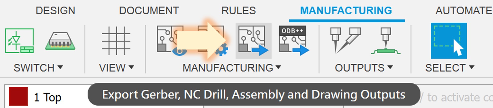
We can check the output data of the board with the CAM Processor icon in MANUFACTURING section.
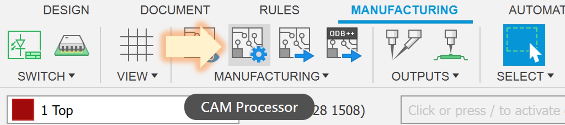
Top Copper(milling), Profile(cutting) and Auto Drill(drilling).
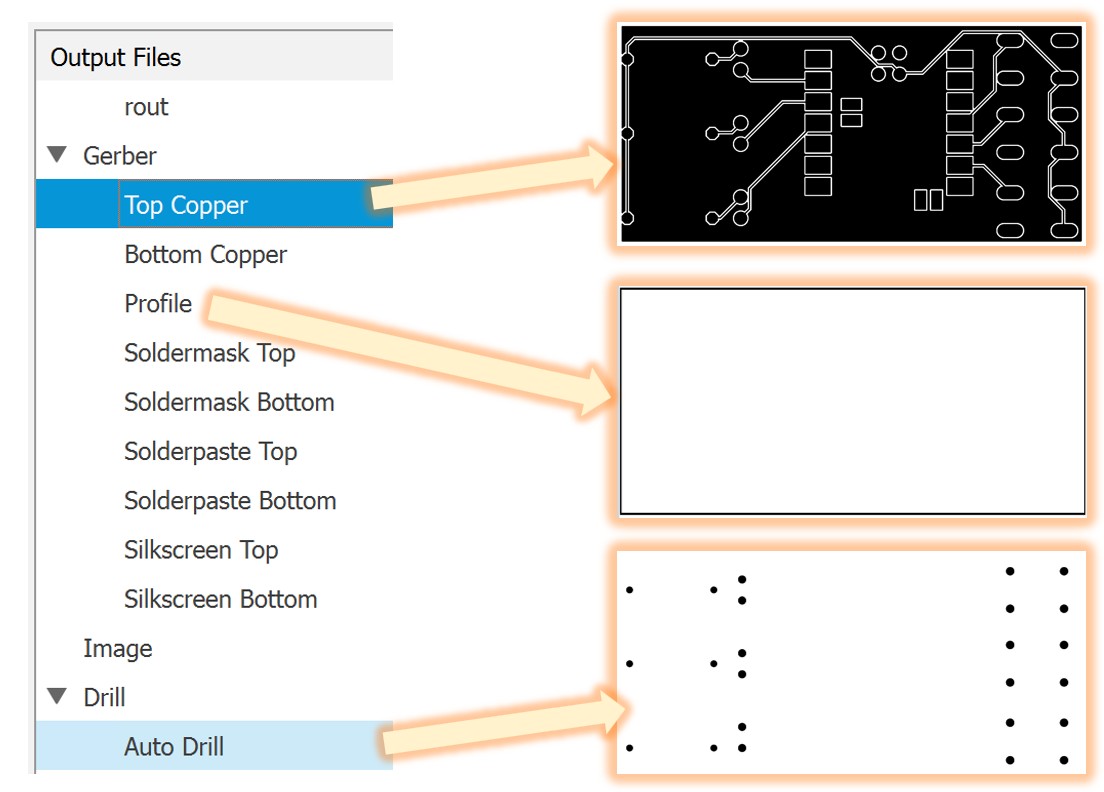
CAM Processor, we can select the data we want and export them separately, or we can export all the file at once with the Export Gerber, NC Drill... icon
Extra:
Simulation
To see the simulation of the real 3D PCB board, we can click on the Push to 3D PCB.
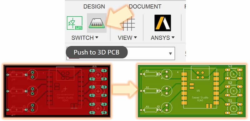
Packages layer visibility, and if you want to see the component on it, turn on the visibility of the Packages layer.
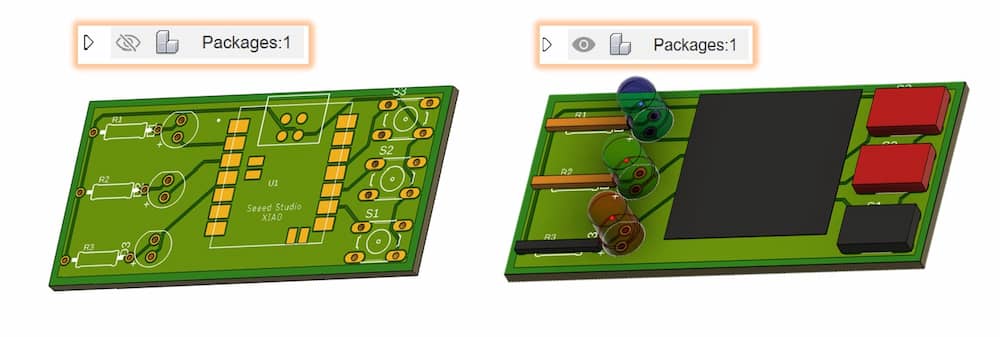
Some components library doesn't have the detail 3D model information. It will just appearing with in cube form in the 3D simulation.
Another design workflow
In the last design, the component I use was THT (Through-Hole Technology) components, which mean it would need to drill holes on the board to let components go through, need to be soldered on the opposite side and the board will be a bigger size.
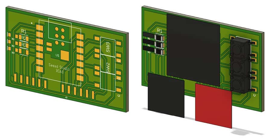
To make the future manufacturing process easier, I will use SMT (Surface Mount Technology) components instead of THT component in the new design.
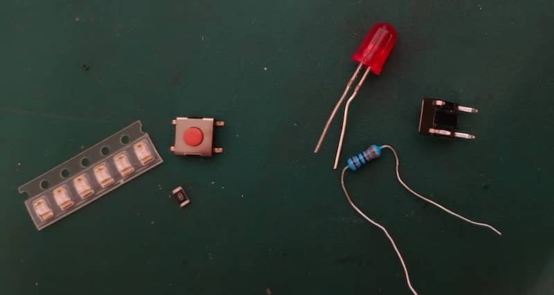
The SMT components(Left) VS THT components(Right)
| Component Name | Library | Quantity |
|---|---|---|
| XIAO-ESP32C3 | Seeed Studio XIAO Series | 1 |
| 2-1437565-8 | Switches | 3 |
| R | Resistor | 3 |
| LED-BLUE | 1206_led | 3 |
| CONN_06 | SparkFun-Connectors | 3 |
Some common component library: https://github.com/usarawgi911/Eagle-libraries/tree/master
| Name | Rule |
|---|---|
| Wire-Wire Clearance | 0.5mm(19.69 mil) |
| Wire-Pad Clearance | 0.5mm(19.69 mil) |
| Wire-Via Clearance | 0.5mm(19.69 mil) |
| Copper Width | 0.5mm(19.69 mil) |
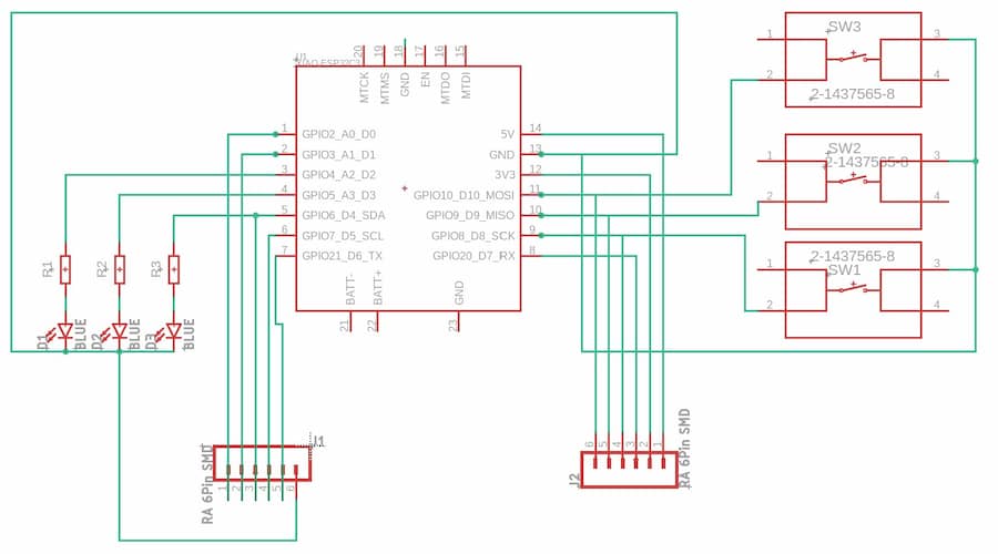
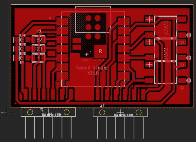
In the new design, I also add 2 pin connector for the further connection.
Here the circuit:
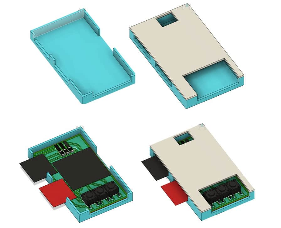
Case Design
Process of case design
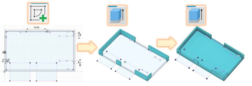
In Fusion360, we can design the case base on the 3D simulation model.
Use p to project the PCB board and compentent outline, draw a case outline which offset from the PCB outline (1mm), and extrude it to form the base of the case.
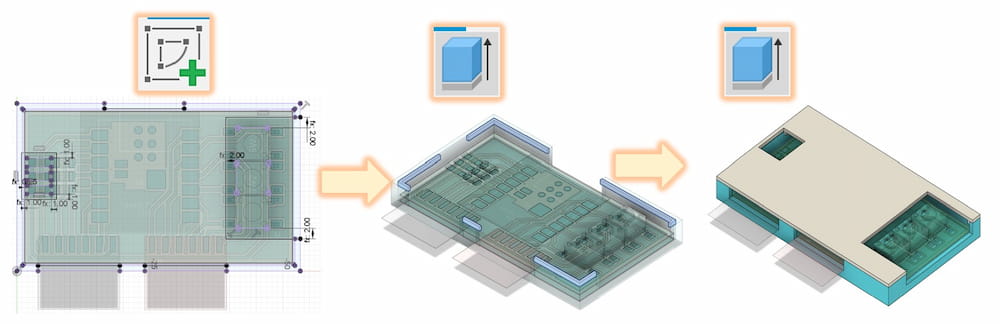
The final simulation of the case, with(up) and without(down) the PCB board