Week6 - Electronics Design
Writing on '2025.2.24'.
Update at '2025.4.23'.
File Sharing
Here's the link about this assignment which included:
Preparation
This week, we have to use and EDA tool to design a development board that uses parts from the inventory to interact and communicate with an embedded microcontroller.
I will use KiCAD as my EDA tool.
First, Download the library and unzip it. The library is provided by Fab Academy.
I download the library by using gitlab command:
git clone https://gitlab.fabcloud.org/pub/libraries/electronics/kicad.git
Step 1 Create a Project and import the library
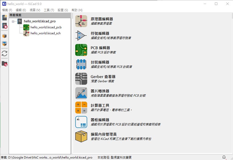
Before adding electronic components to your schematic, the libraries of the components from fabacademy needs to be installed first. Go to the "Manage Symbol Libraries" and add the library we just downloaded.
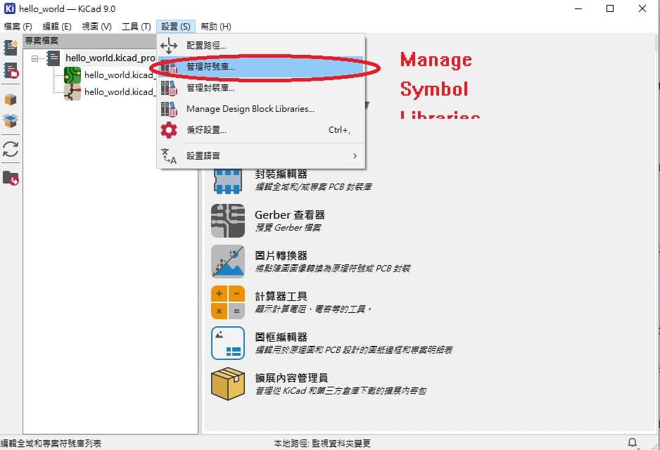
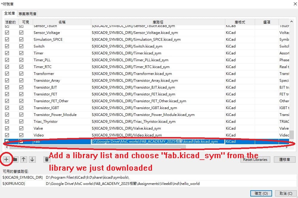
Add the library to KiCad
Then, choose "Manage Footprint libraries" and add to KiCad.
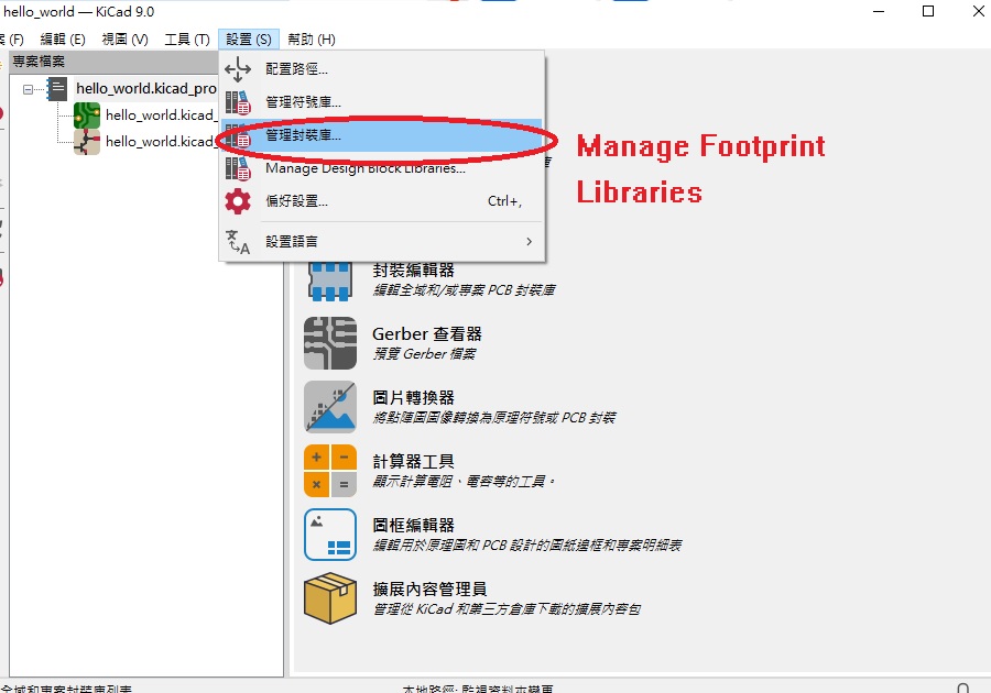
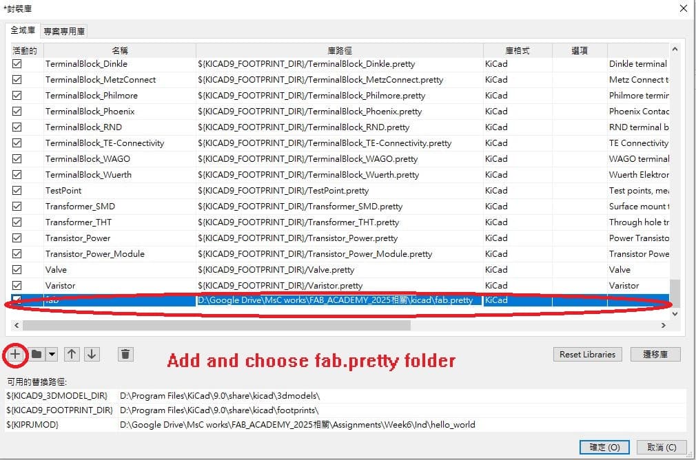
Now, we can edit sch file for designing circuit.
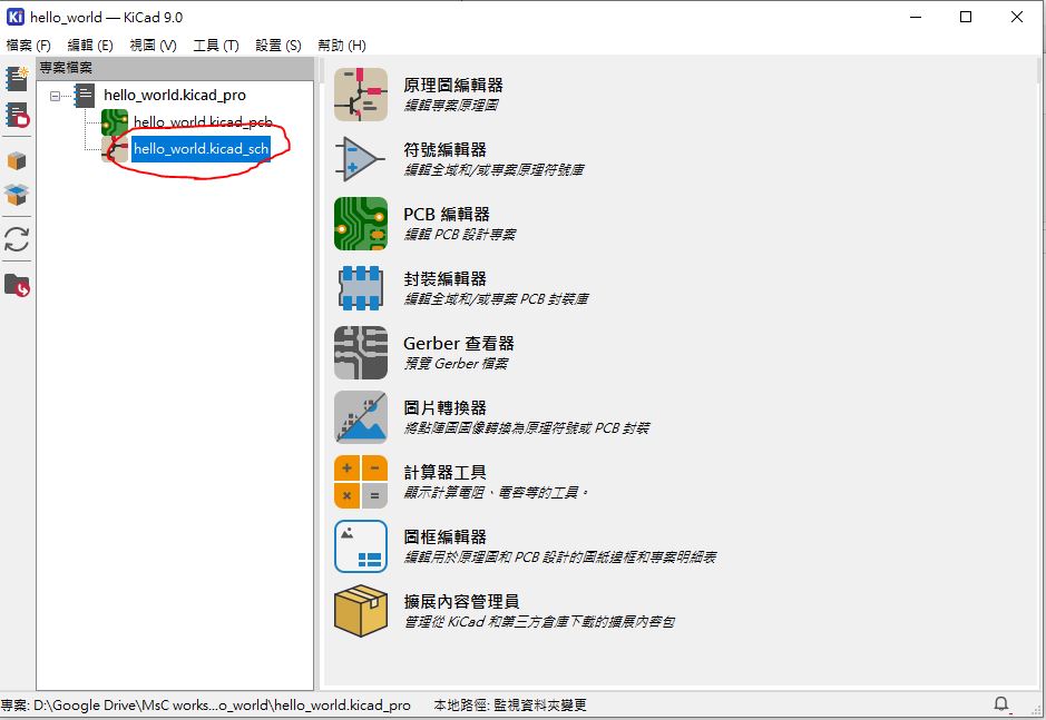
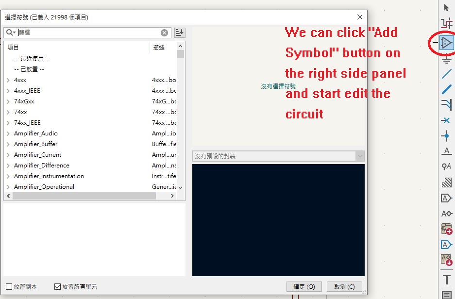
Then, go to the following Interface(.pro file) and go to Settings->Configure Path.
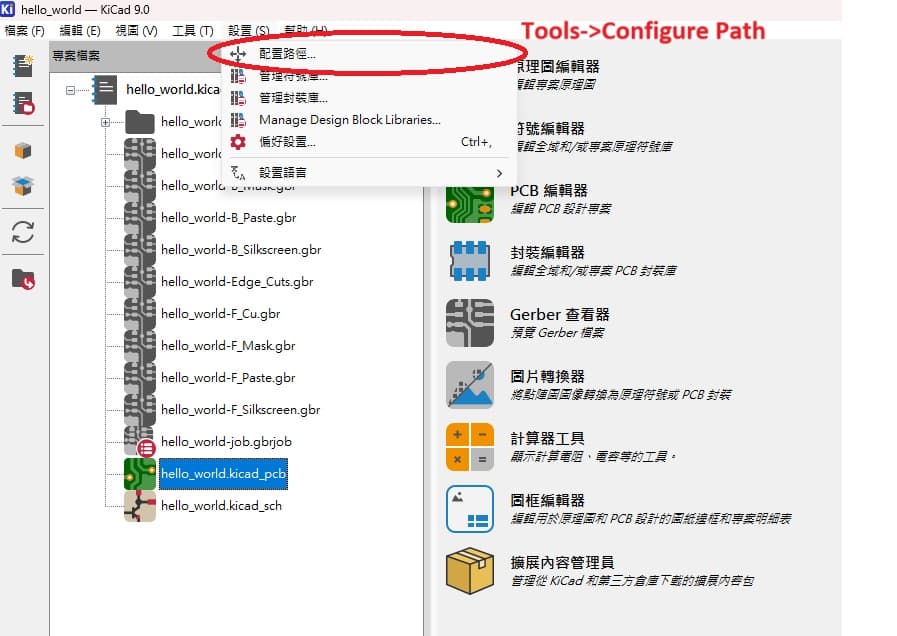
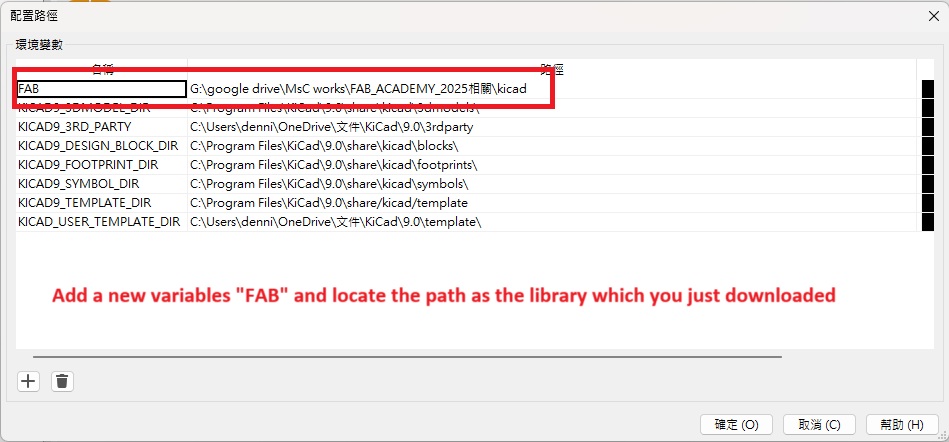
Then, add a new path and link the path to the library which we just downloaded. The 3D view will not be shown if this step is skipped.
Step2 Drawing sch file
Now, you can add the main MCU to the sch file.
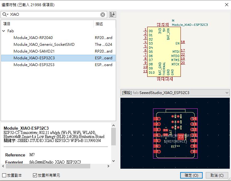
In my case, I add one LED(1206), one switch, and two pinsockets(6 pins) from the Fab library.

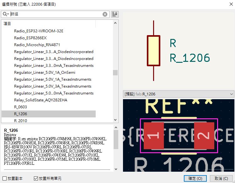
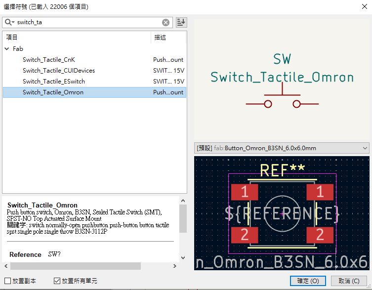
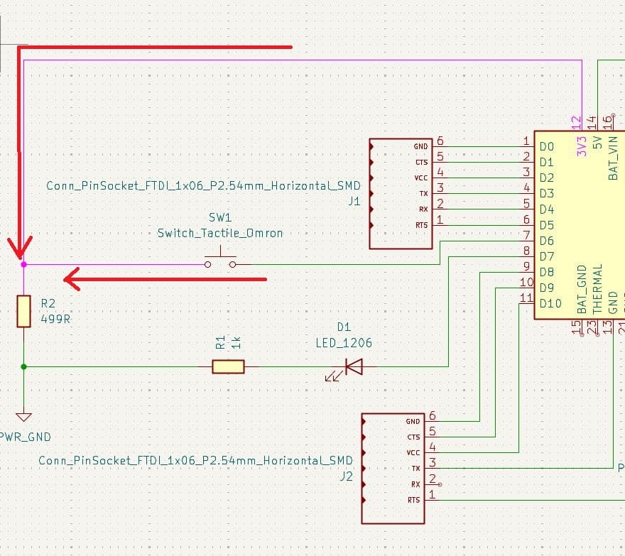
Then I design a simple circuit with pull-down resistor (499ohm) to switch for prevent from short circuit and burn out the circuit.
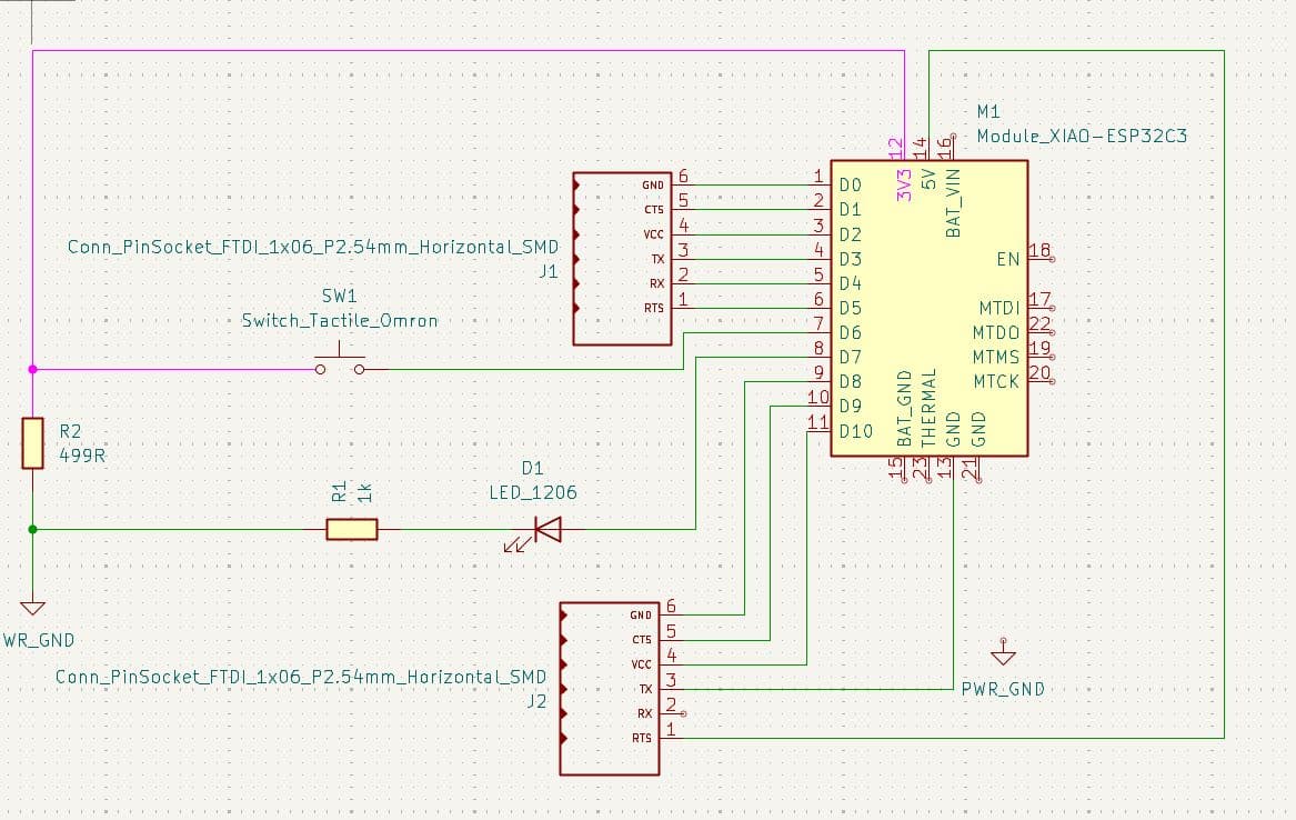
After the wire connection, the circuit is finished.
Circuit Simulation
Simulation
Before forming PCB, I built a simulation in wokwi which's circuit is same as the designed development board in this assignment.
void setup() {
  Serial.begin(115200);
  pinMode(D6, INPUT);
  pinMode(D7, OUTPUT);
}

void loop() {
  digitalWrite(D7, LOW);
  Serial.println(digitalRead(D6));
  if(digitalRead(D6) == HIGH){
    digitalWrite(D7, HIGH);
  }else{
    digitalWrite(D7, LOW);
  }
}
When the button is pressed, the LED will turn on. When the button is released, the LED will turn off.
Step3 Drawing PCB layout
Then, click "update Schematic to PCB":
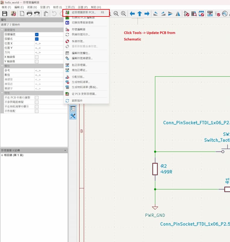
Then you will have the first view of your PCB
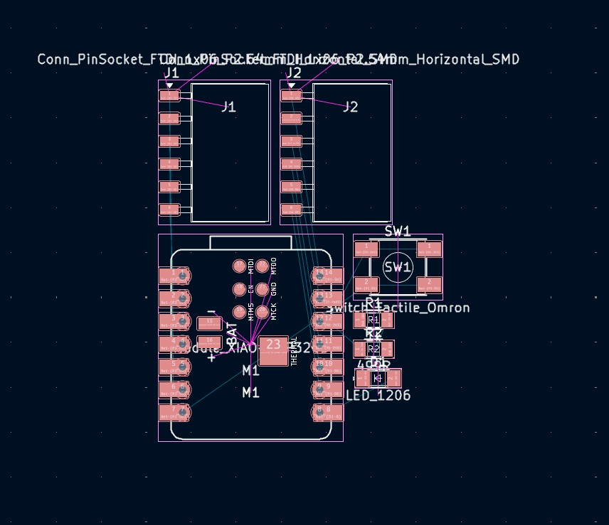
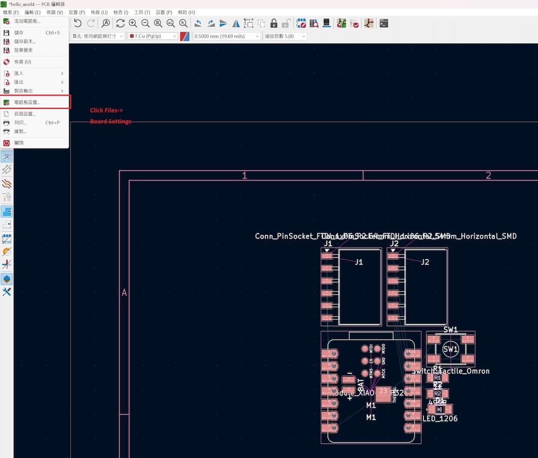
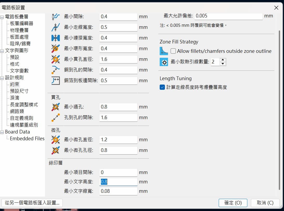
Adjust the PCB design rules.
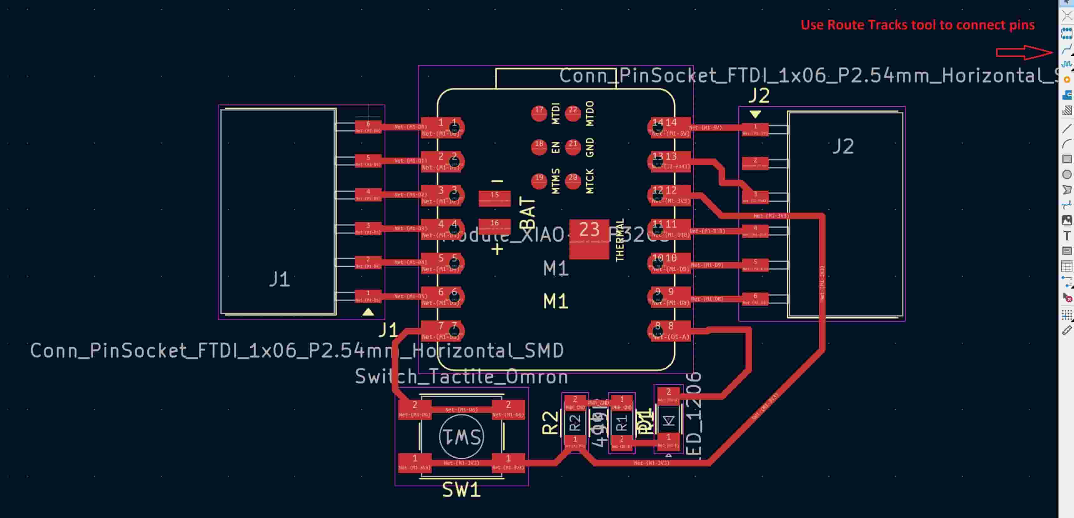
Use Route tool to link the routes.
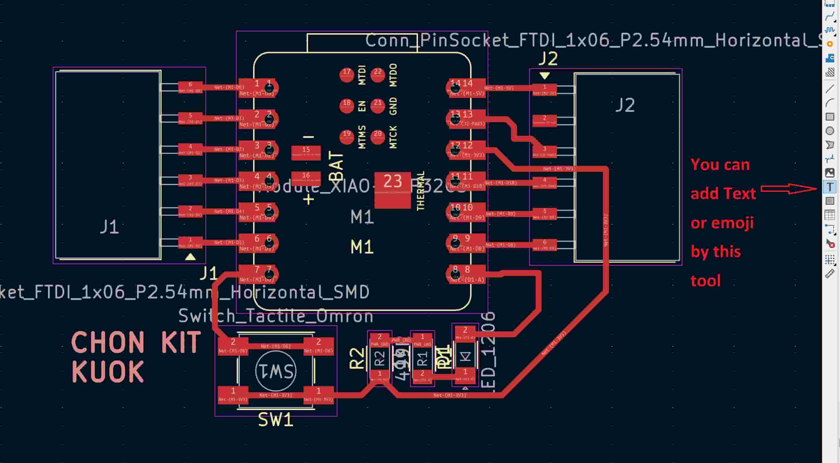
I can also add texts/emoji to the circuit board design.
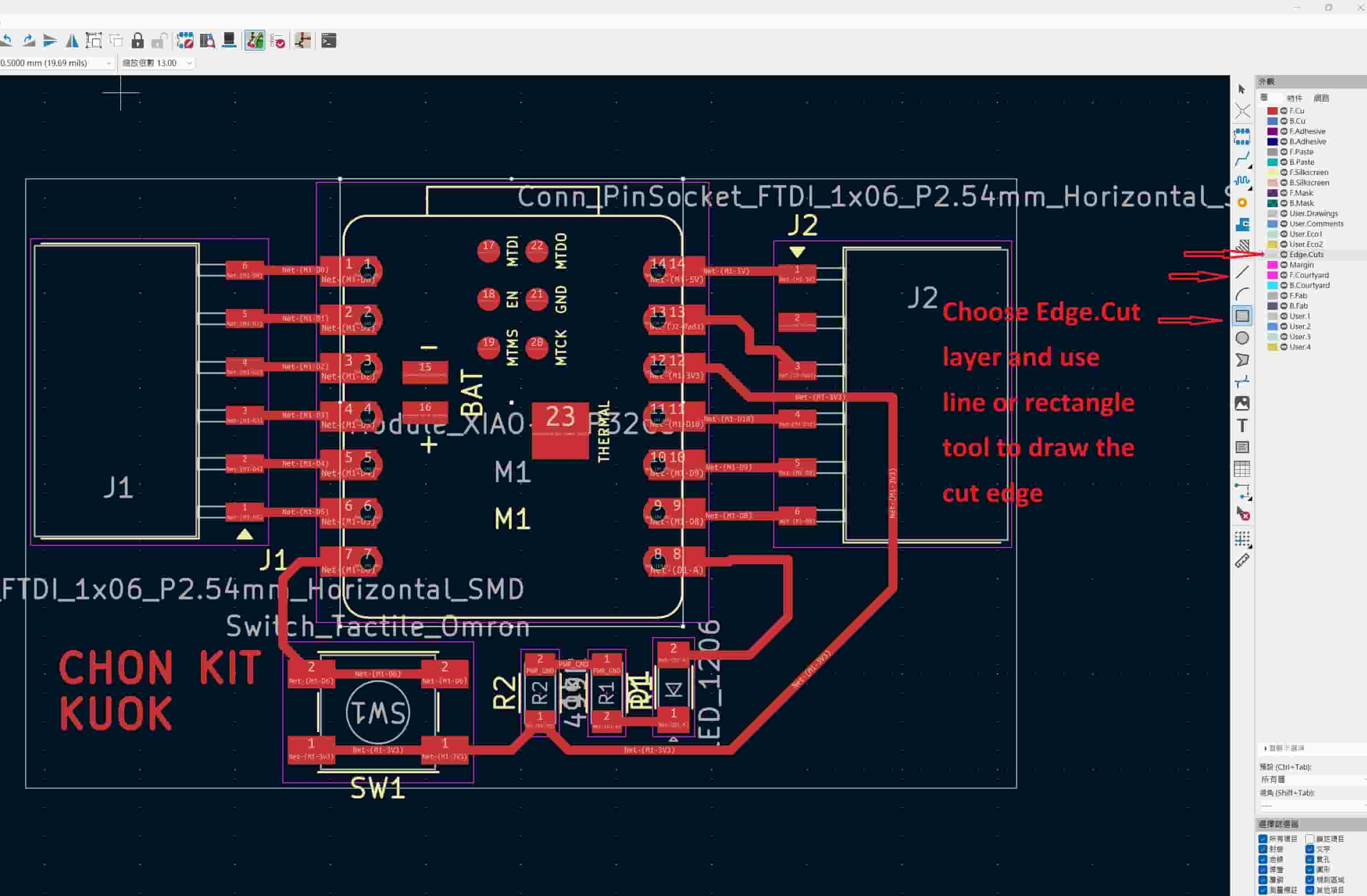
After finishing the trace layer, change to cut layer (Choose Cut Edge) and draw the boarder of the circuit board.
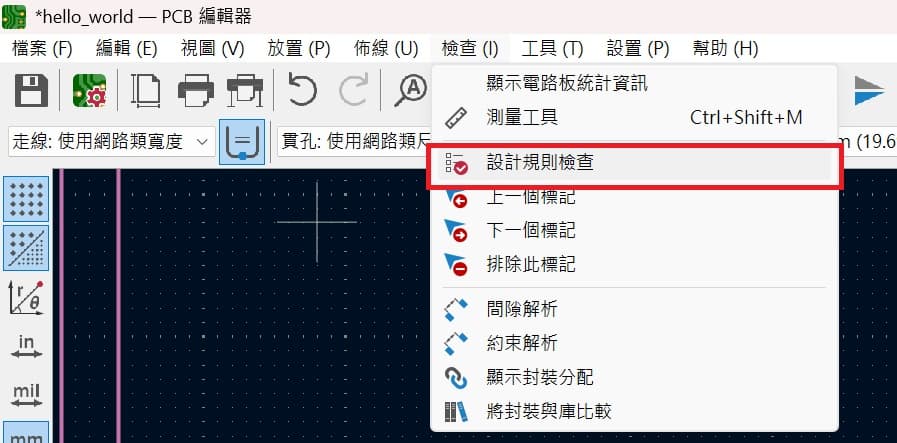
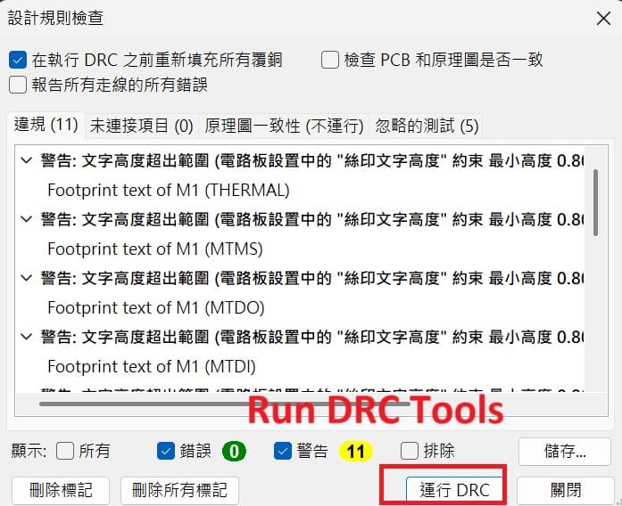
Before export the layout files, you can use the DCR tool to check the design of circuit board is legal or not.
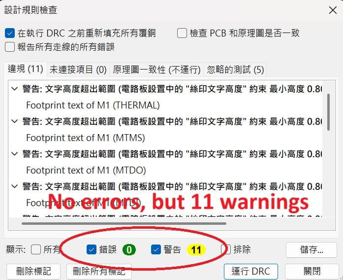
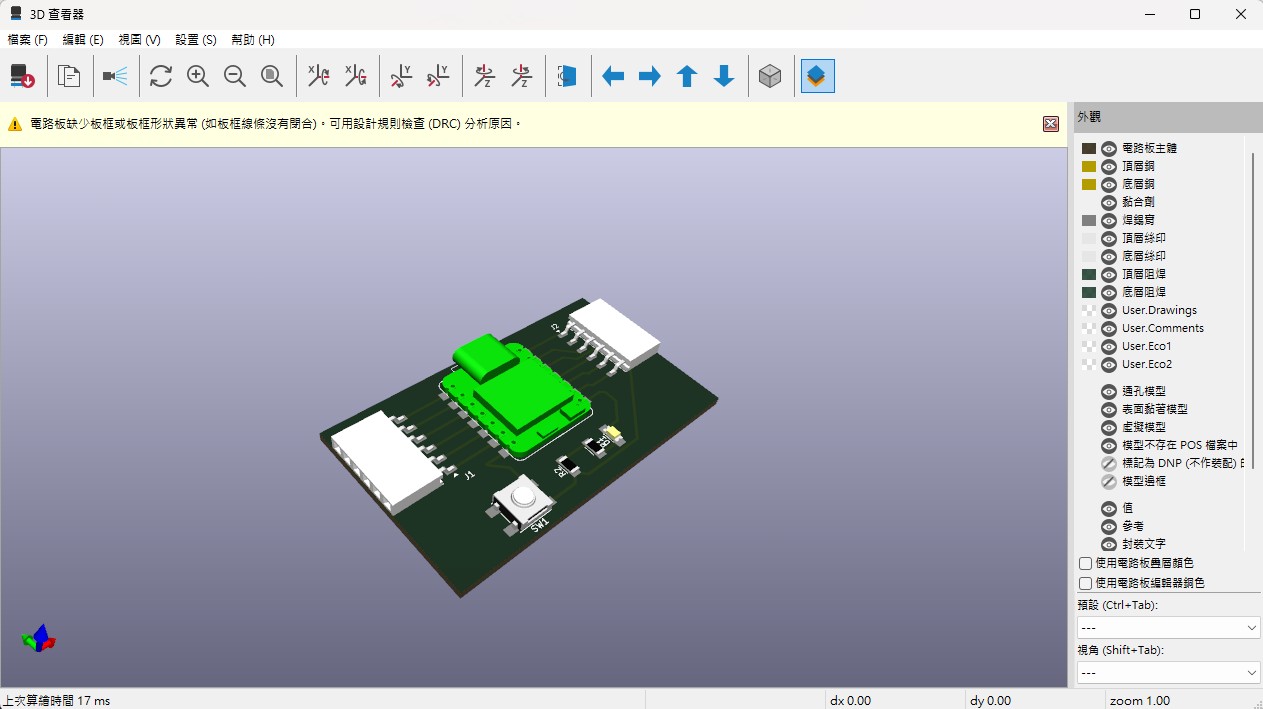
I also do the 3D simulation of the circuit board:

Then, I will export the files to Gerber files.
3D viewer can be opened in PCB editor.

We will use the Mod the generate the cutting route for CNC. First I have to transfer the Gerber files to PNG. A online tool Gerber2Png will be used.
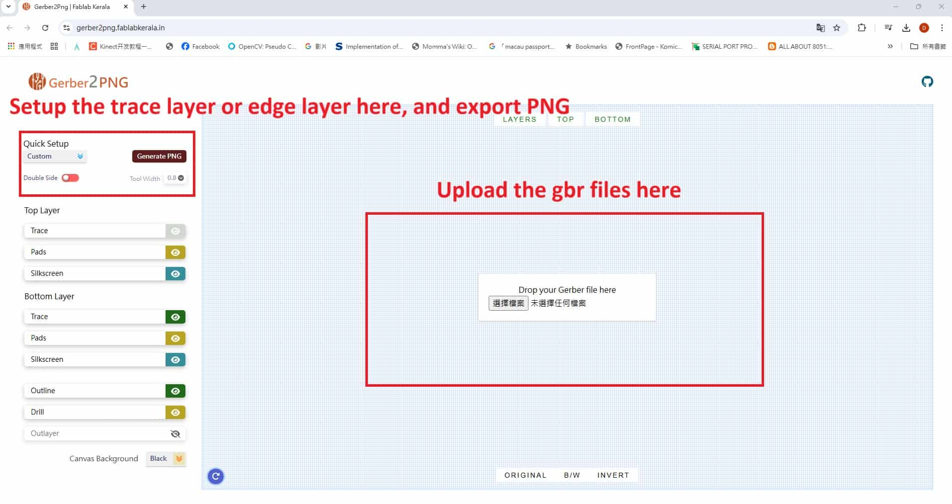
Upload the gbr files(In my case, I will upload F_Cu.gbr and Edge_Cut.gbr)
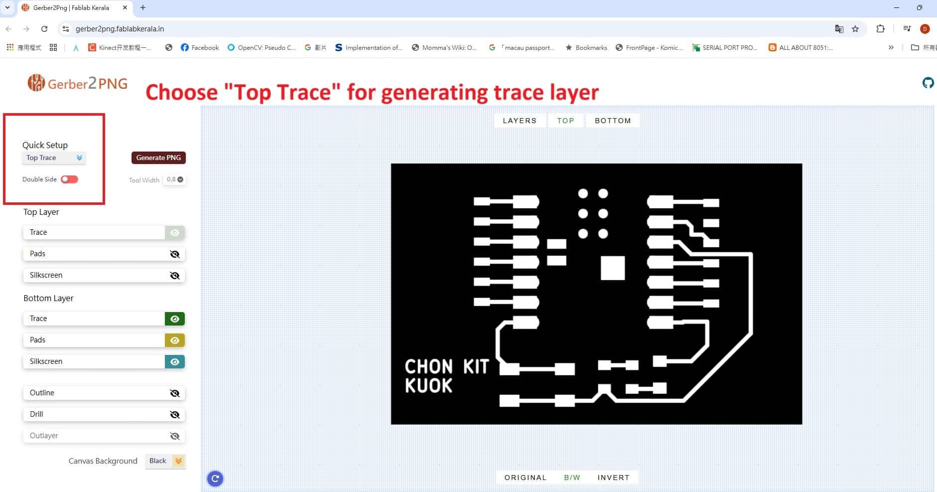
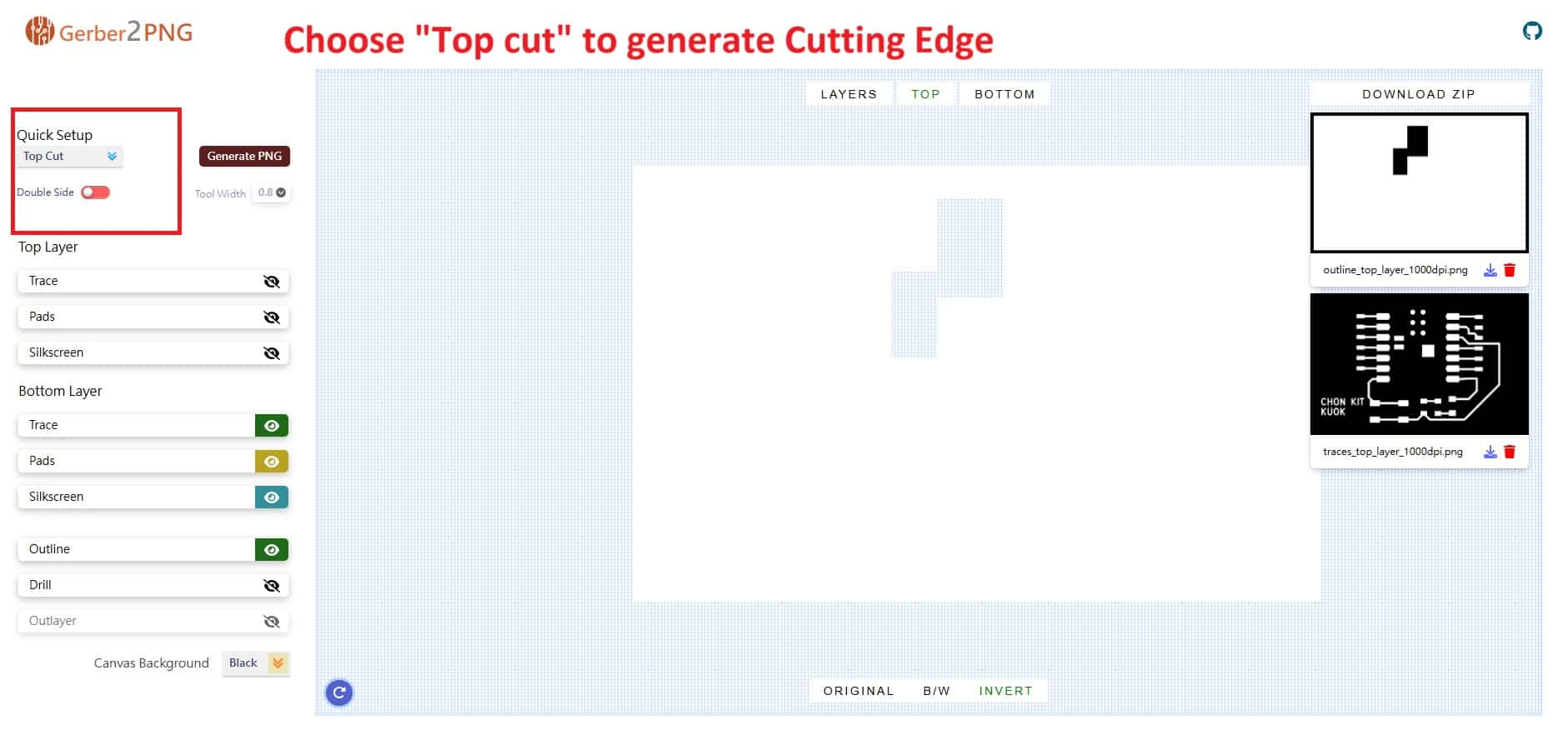
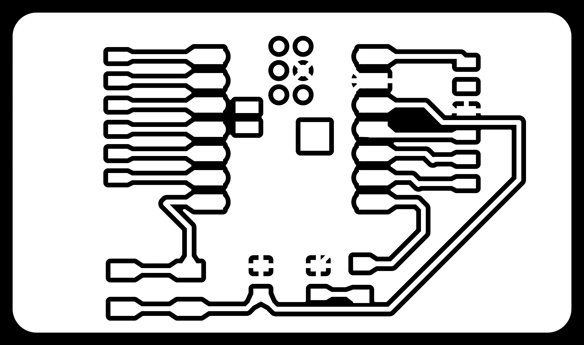
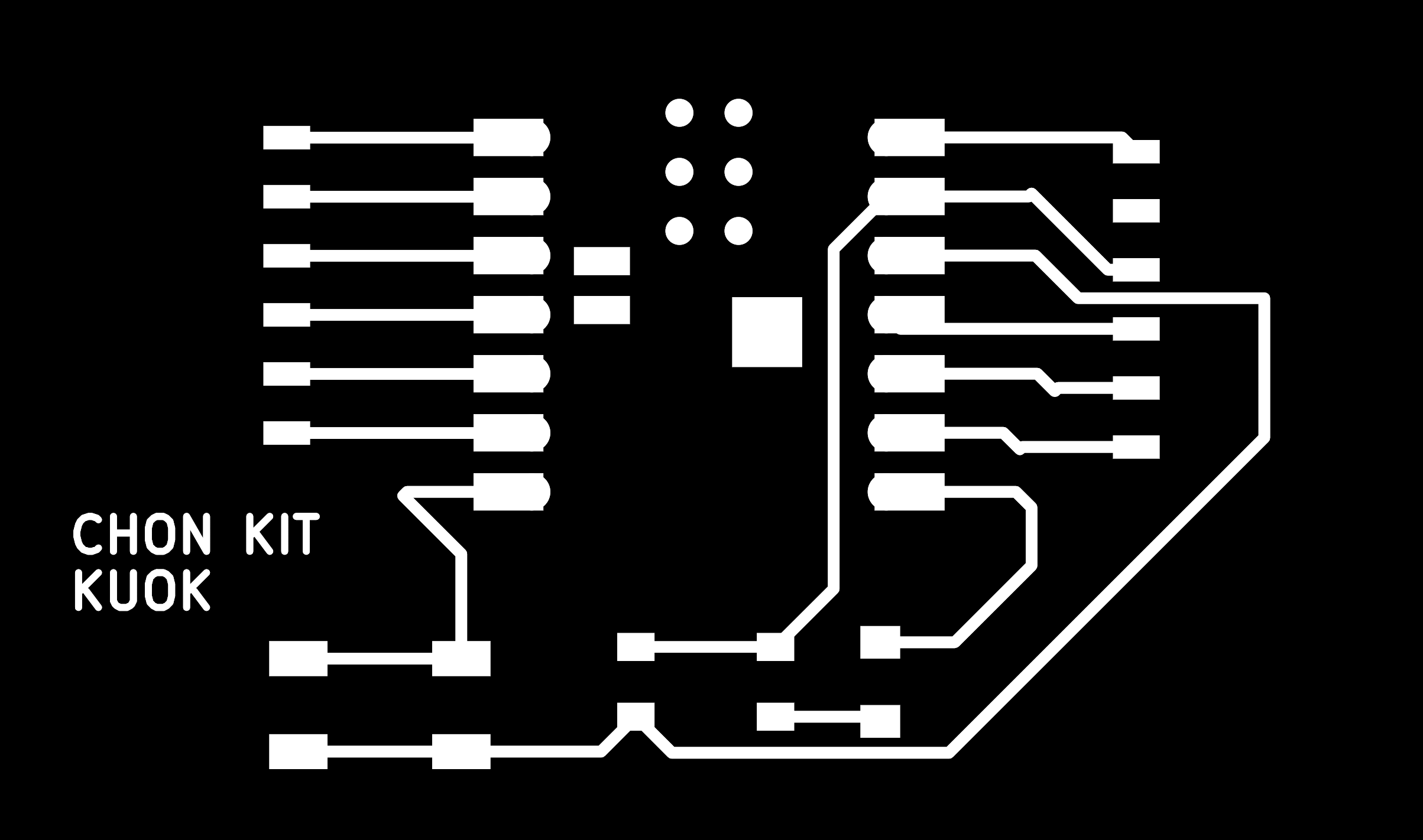
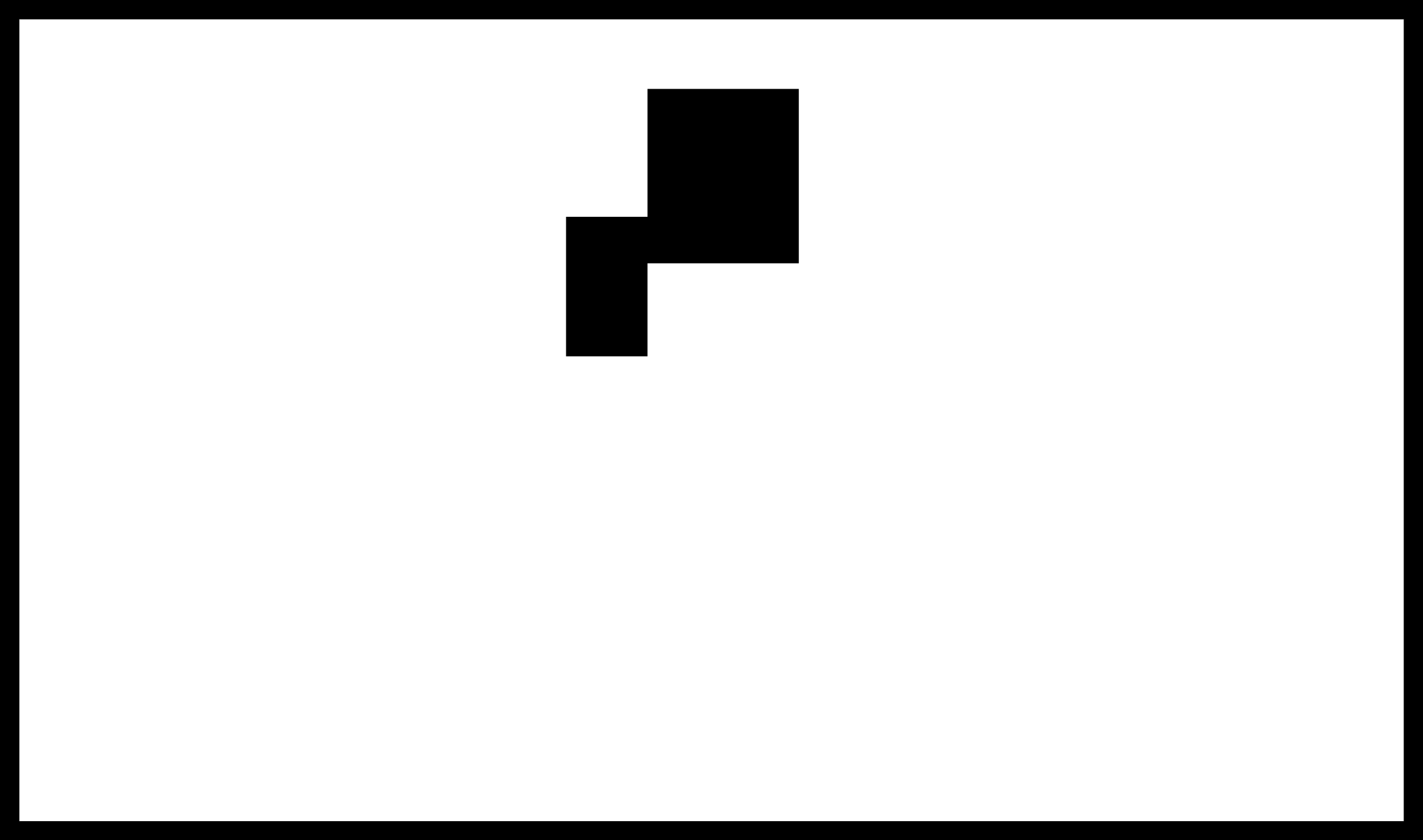
Finally, 2 png files are generated. One of the png is used for tracing and another one is for cutting edge.
Update PCB
Update at '2025.3.18'.
In order to meet specifications of PCB production to finish one of the target of Week 8 group assignment, some process should be added.
Turn the edge corner of PCB board to round angle
Choose Edge.Cuts layer and select the boarder, right click to open the context menu, set 3mm radius rounded corner for the board boundary.
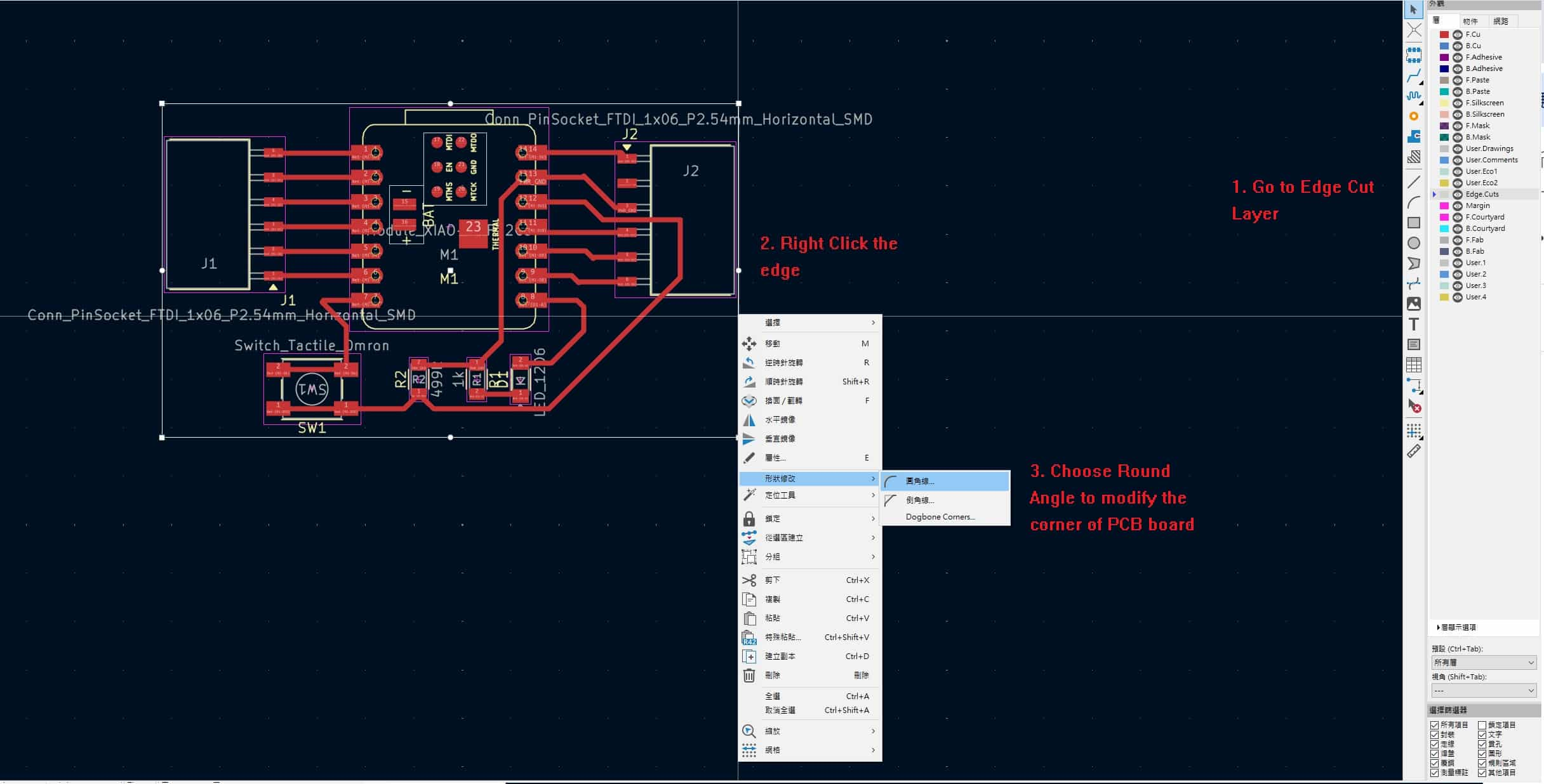
Then, the corner of the PCB board will turn to rounded angle.
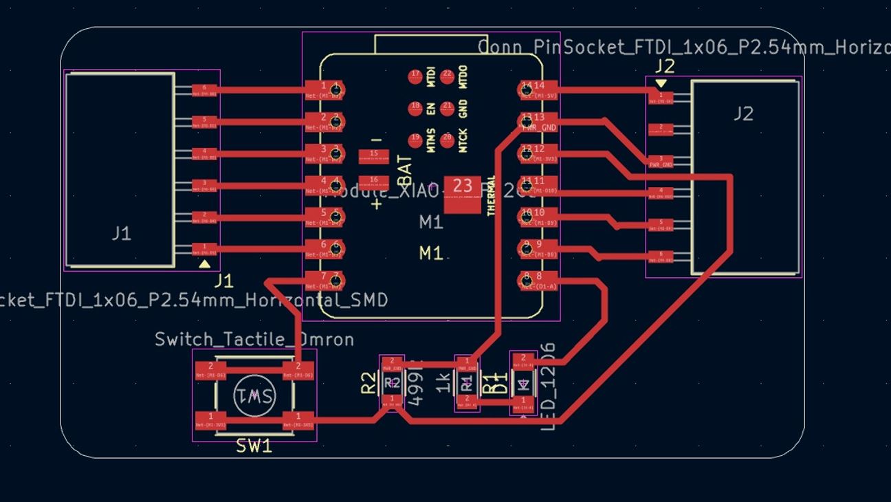
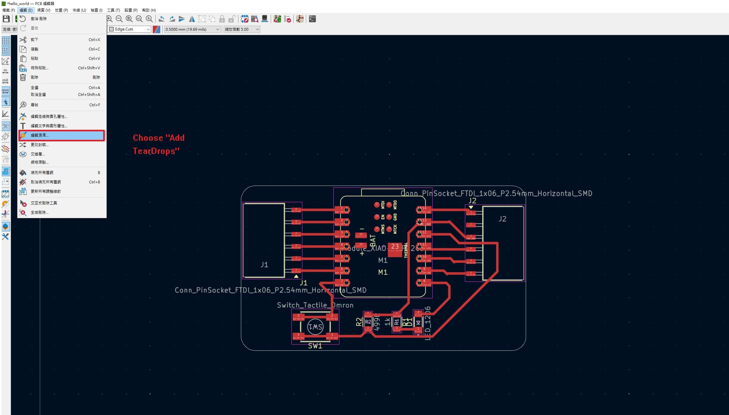
Adding Teardrops
- Select "Edit"->"Add TearDrops" from the top menu.
- In the "TearDrop Settings" windows, configure teardrop parameters which is suitable for CNC milling
- Click "Apply" to observe the effect
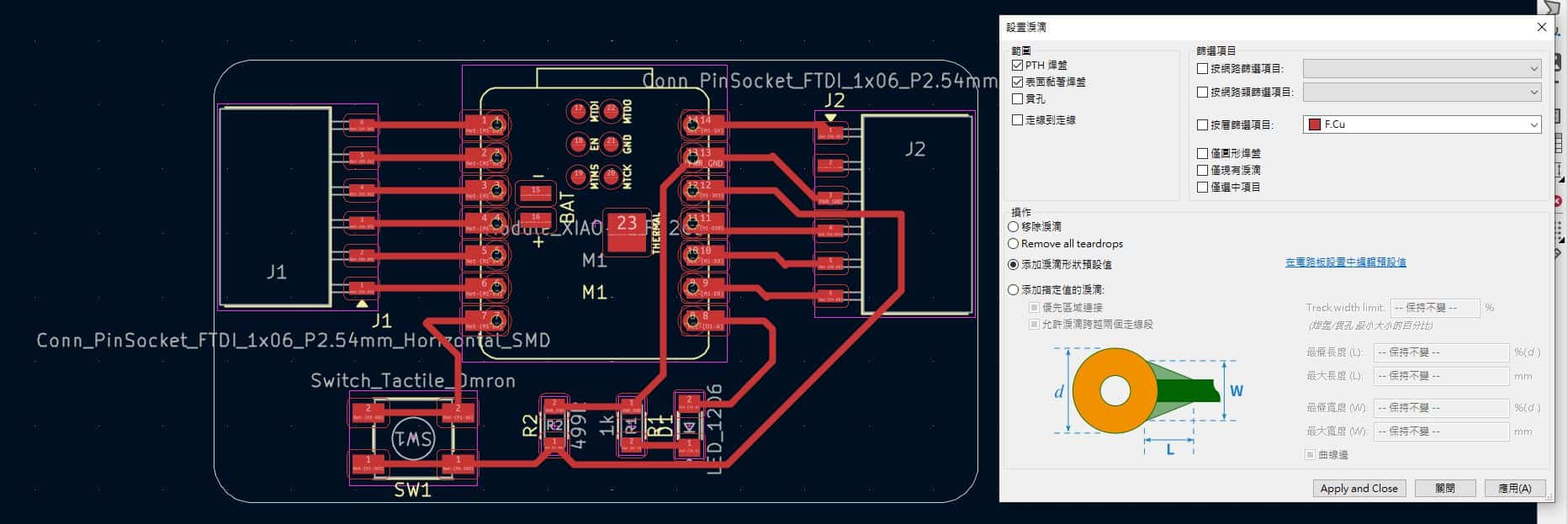
The actual effect will coming out after finishing the copper-filling step.
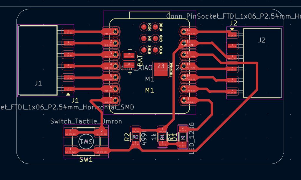
Adding Copper Fill
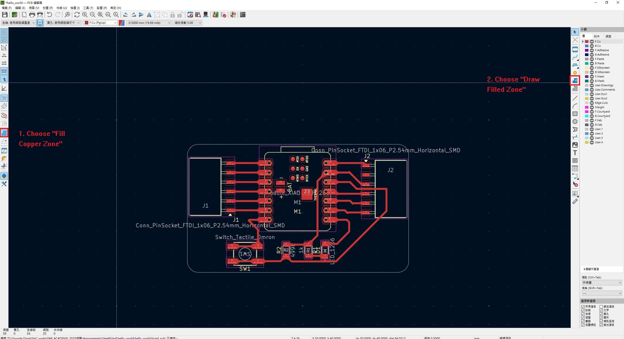
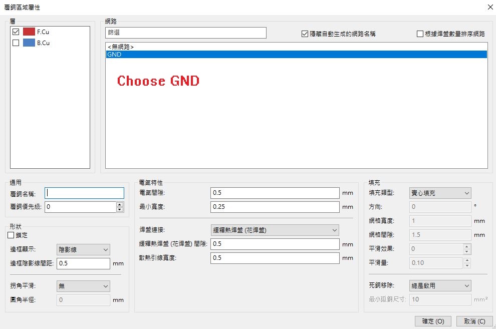
- Select F.Cu layer, select the "Draw Fill Zone" on the right and choose the filling area. The properties windows will appear and select
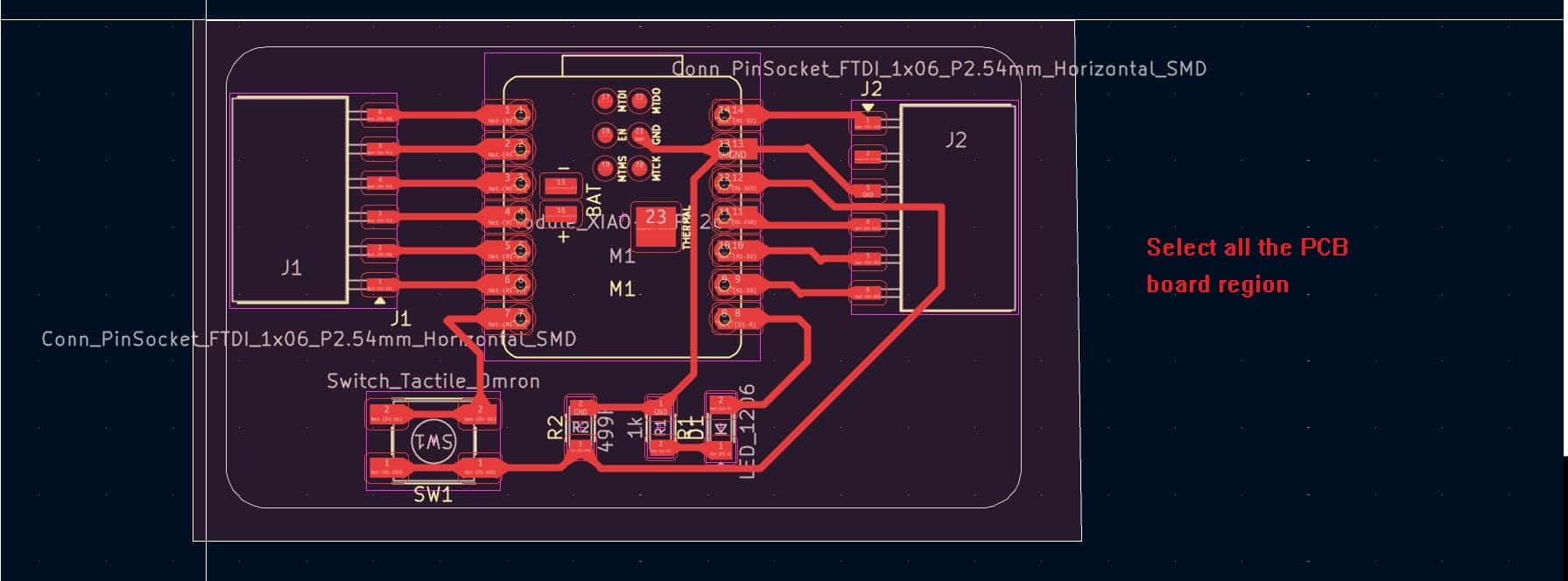
GNDin the network. - Select the copper fill area. In this case, I choose surrounding the entire PCB board.
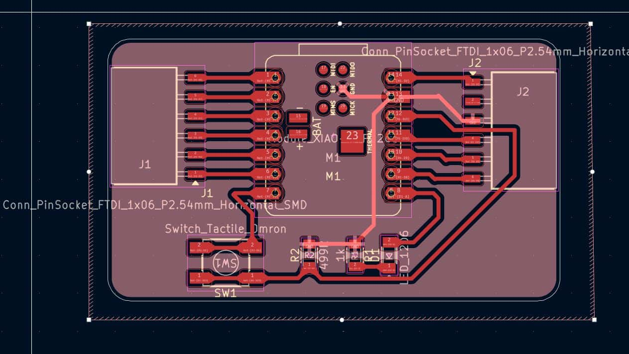
- Press shortcut Key 'b' or click menu "Edit"->"Fill All Zones"
- Ensure the copper fill area maintains sufficient distance from signal lines
After finishing the copper fill step, GND parts are connected together.
Viewing in the 3D viewers:
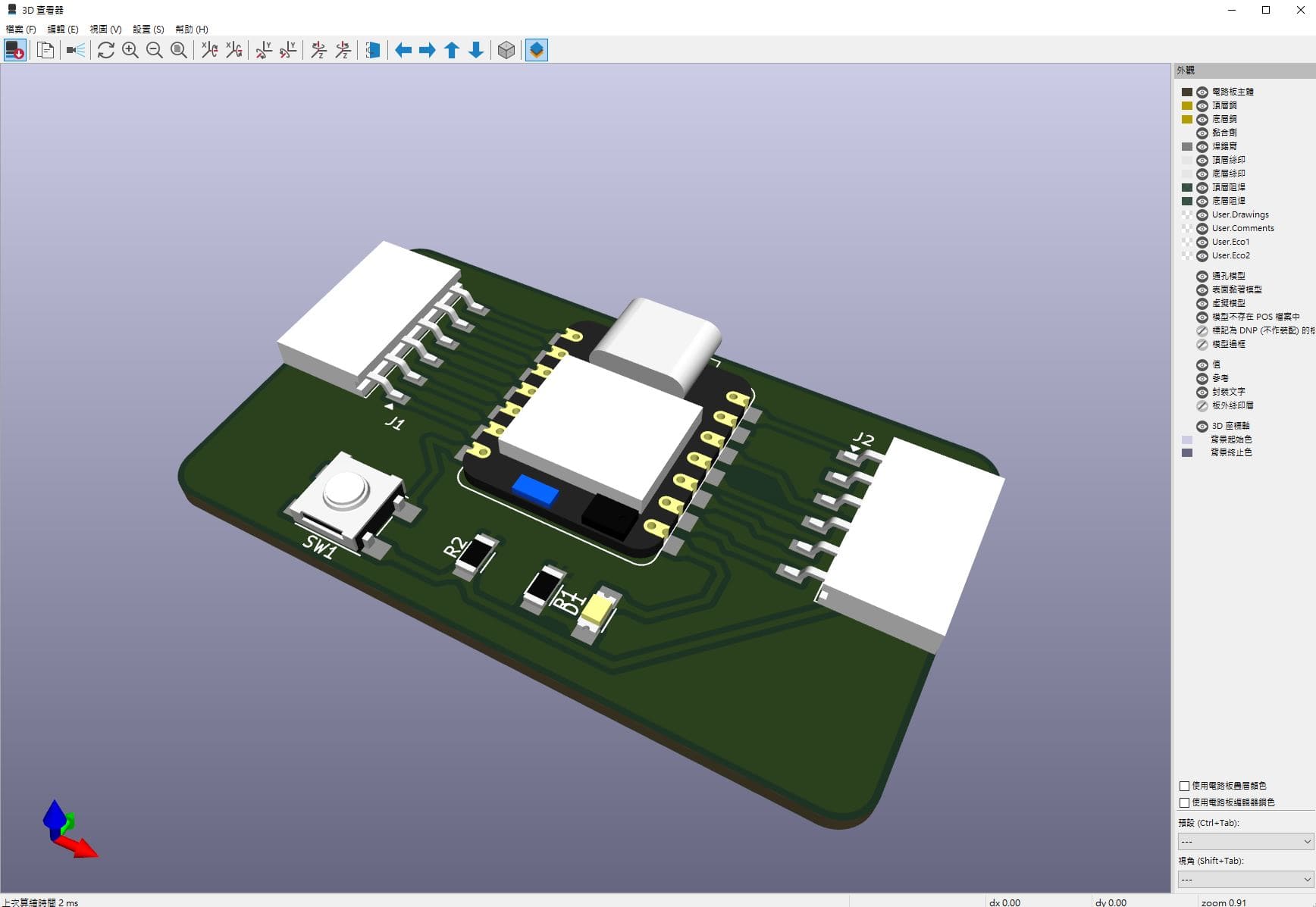
Updated PCB layout
Upload the renew gbr files (F.Cu and Edge Cut layers) to Gerber2Png. And generate the new png image for Mod to generate G.code files.
