Week8 - Group Assignment - Macao
File Sharing
Task of group assignemnt
- Characterize the design rules for your in-house PCB production process
- Submit a PCB design to a board house
Design Rules for in-house PCB production process
Machines and tools
In this assignment, We will do the electronic production by a machine MODELA MDX-50 Benchtop CNC Mill.
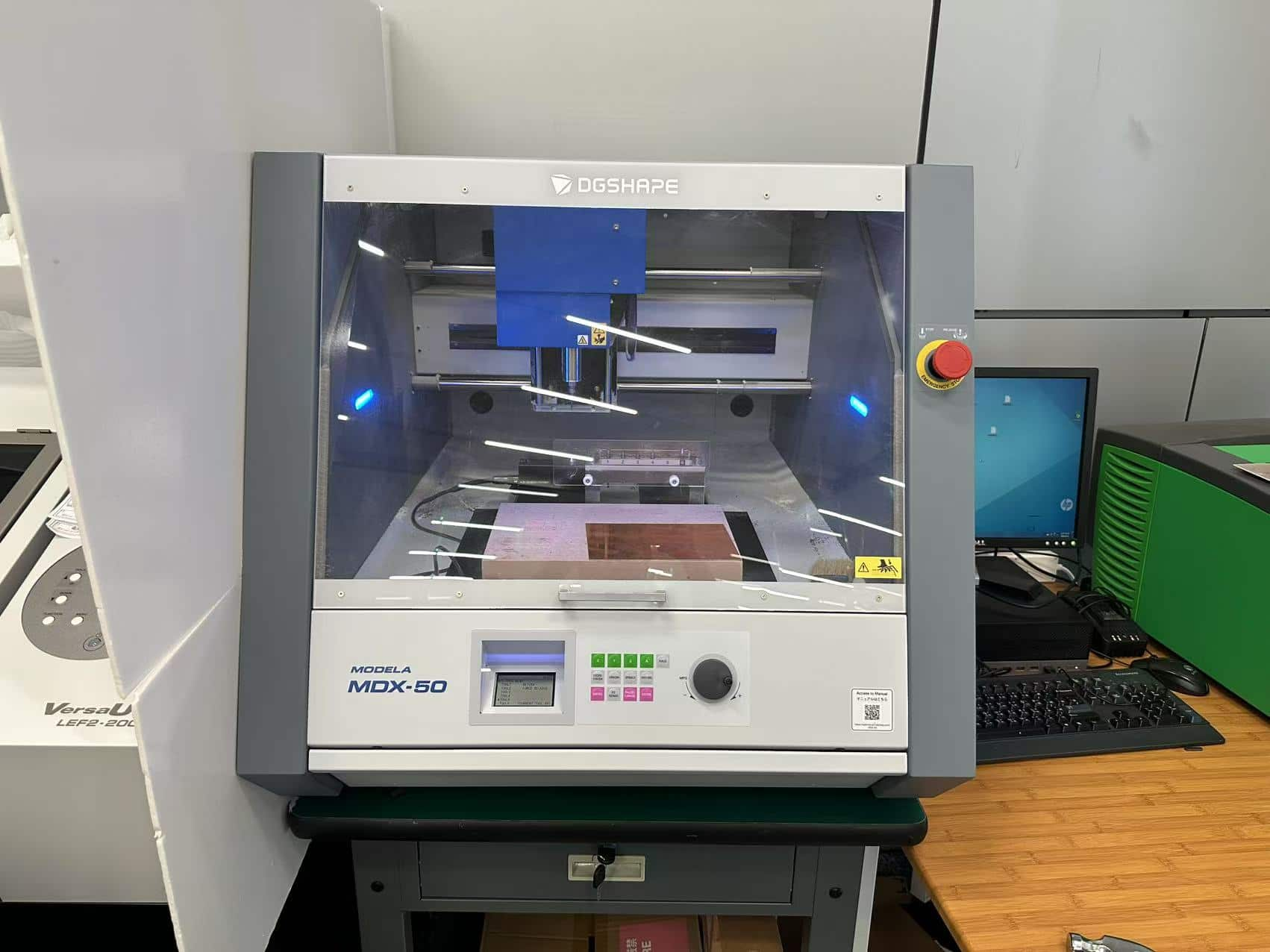
This machine is used for making accurate protoypes. For example, milling a mold(which is week 13 assignment).
Here's the specification of MDX-50 machine.
| Max Working Area(X,Y,Z) | Table Size | Tool Shaft Diameter | Number of tools in toolchanger | Max Feed Rate | Mechanical Resolution | Cutter Rotation Speed | Control Software |
|---|---|---|---|---|---|---|---|
| 400 x 305 x 135 mm | 400 x 305 mm | 3 mm, 4 mm, 6 mm, 1/8", 1/4" | 6 (one of the tools is the detection pin) | 60 mm /sec | 0.01 mm | 4500 - 15000 rpm | Roland V-Panel, SRP Player |
There're lots of milling tool in our lab.
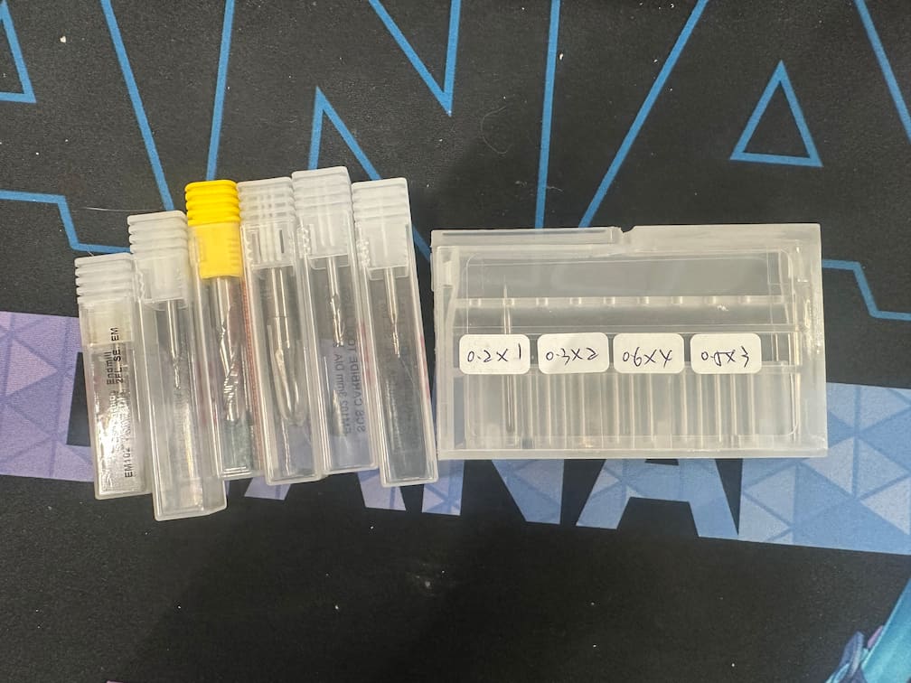
In this assignment, we will use the following tools for PCB milling.
- V-bits. 6 * 20 * 0.3 V-bit for tracing
- Ball end tool. 1.5 * 0.3 for outline cutting
Materials
We use a standard copper fiber boards.
- Material: FR-1/FR-4 Epoxy Glass Fiber Sheet
- Thickness: 1.6mm
- Thickness of copper layer: 35μm(1oz)
Milling Parameters
We tested the different tools to find out the optimized parameters for our CNC machine. The parameters are shown as below.
| Parameters | V-Bits(Tracing) | Ball End(Outline Cutting) |
|---|---|---|
| Feed Speed | 4mm/s | 4mm/s |
| Spindle Rotation Speed | 14000rpm | 14000rpm |
| Offset Number | 4 | 4 |
| Offset Stepover | 0.2 | 0.2 |
| Cut Depth | 0.23mm | 0.45mm |
| Diameters of Tool | 0.3mm | 1.5mm |
Result
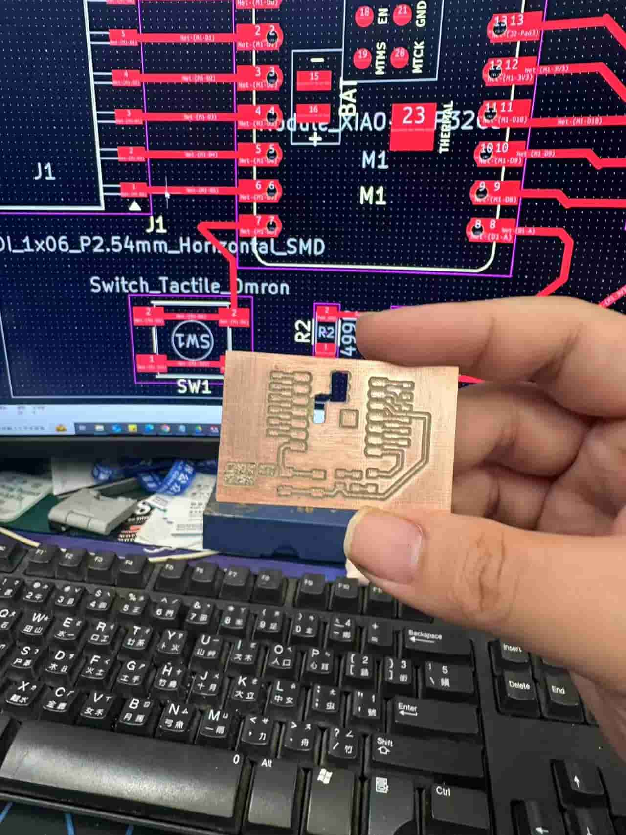
The result of milling parameters can be used for PCB CNC milling, the effects are shown as below.
Submit a PCB design to board house
Preparation
We have designed a PCB development board in week6 assignment.
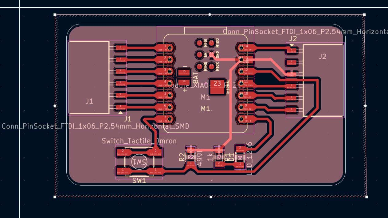
According the process of export gbr files, we have generated 2 gbr files.
- F_Cu.gbr (for tracing)
- Edge_Cuts.gbr (for outline cutting)
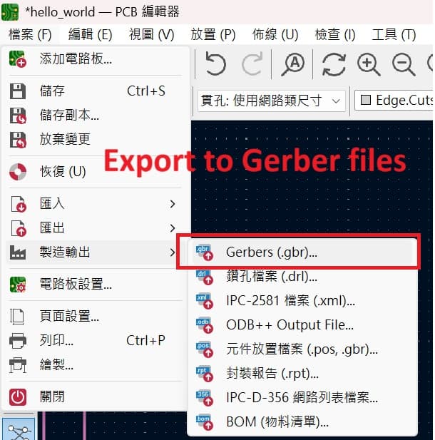
These files can satisfy the essentials files for milling PCB by our machine. But it's not enough for the PCB production.
More gbr files are needed for PCB production.
- B_Mask.gbr (Drill file, a layer file for drilling holes)
- F_Mask.gbr (Solder Mask)
- F_Silkscreen.gbr (Silkscreen layer, for showing captions or text on the PCB board)
I have no idea about PCB before doing this assignment, I ask Deepseek about the B_mask, F_mask and Silkscreen.
Drill File
A Drill file for a PCB (Printed Circuit Board) is a type of file used in the manufacturing process to specify the locations, sizes, and types of holes that need to be drilled into the PCB. These holes are typically used for mounting components, vias (electrical connections between layers), and other mechanical purposes.
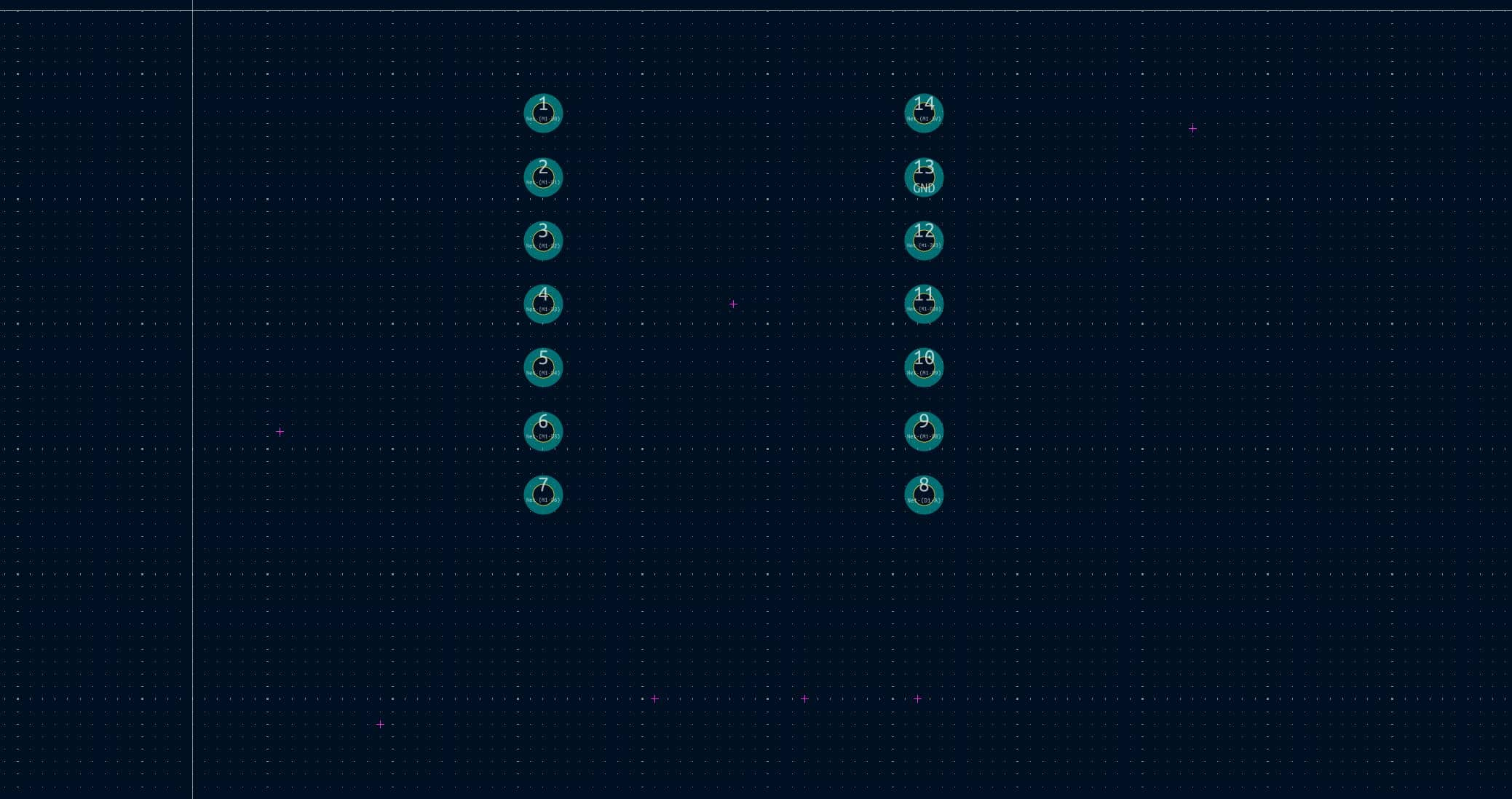
Key Information in a Drill File:
-
Hole Locations: The X and Y coordinates of each hole on the PCB.
-
Hole Sizes: The diameter of each hole.
-
Hole Types: Differentiates between plated (for vias) and non-plated holes (for mounting).
-
Tool Codes: References to specific drill bits used for different hole sizes.
Common Formats:
-
Excellon Format: The most widely used format for drill files. It typically has extensions like .drl, .txt, or .drd.
-
Gerber Format: Sometimes, drill information is included in Gerber files, but it's more common to have a separate drill file.
Solder Mask
A solder mask (or soldering mask) is a thin, protective layer of polymer applied to the copper traces of a Printed Circuit Board (PCB). Its primary purpose is to prevent solder from bridging between conductive traces during the soldering process, which could cause short circuits. It also protects the copper from oxidation, contamination, and environmental damage.
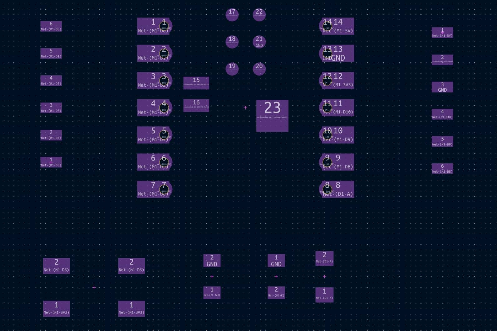
Key Functions of a Solder Mask:
-
Prevents Solder Bridging: During soldering, the solder mask ensures that solder only adheres to the exposed pads and not to the adjacent traces, preventing unintended electrical connections.
-
Protects Copper Traces: The solder mask shields the copper traces from oxidation, moisture, dust, and other environmental factors that could degrade the PCB over time.
-
Improves Durability: It adds a layer of mechanical protection, reducing the risk of scratches or damage to the copper traces during handling or assembly.
-
Insulation: The solder mask acts as an electrical insulator, preventing accidental contact with conductive parts of the PCB.
-
Aesthetic Enhancement: Solder masks are often colored (most commonly green, but also available in red, blue, black, white, etc.), which helps in identifying different PCBs and improves their visual appearance.
Silkscreen
Silkscreen on a PCB (Printed Circuit Board) refers to the layer of text, symbols, logos, or other markings printed on the surface of the board. It is primarily used for identification, assembly guidance, and debugging purposes. The silkscreen is typically applied using ink (often epoxy-based) and is usually white, though other colors like yellow, black, or red can also be used depending on the PCB design and requirements.
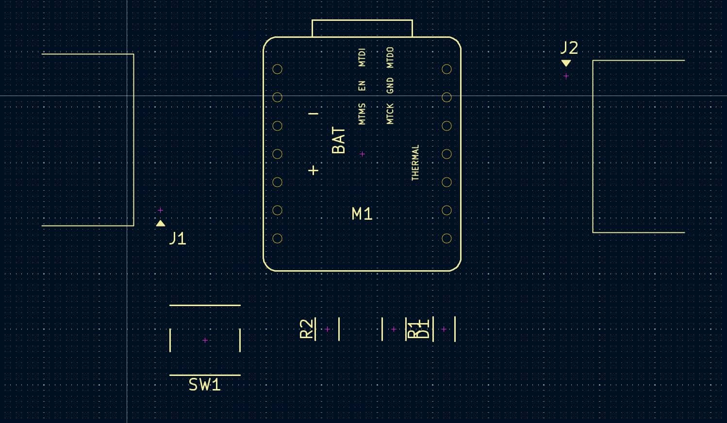
Purpose of Silkscreen:
- Component Identification:
-
Labels for component reference designators (e.g., R1, C2, U3) to help identify components during assembly and debugging.
-
Polarity markings for components like diodes, capacitors, and ICs.
- Assembly Guidance:
-
Indicates the orientation and placement of components (e.g., pin 1 indicator for ICs).
-
Provides instructions for assembly, such as "THIS SIDE UP" or "NO COMPONENTS."
- Debugging and Testing:
- Marks test points, connectors, and other critical areas for easier troubleshooting.
- Branding and Aesthetics:
-
Includes company logos, product names, version numbers, or other branding information.
-
Enhances the visual appeal of the PCB.
- Regulatory Information:
- Displays certifications, safety warnings, or compliance marks (e.g., CE, RoHS).
After studying more about the PCB production, I generate 5 files for PCB production and send the files to PCB-house for producing.
Producing PCB at PCB-house
My classmate Lei Feng introduces a PCB producer company - JLC Technology Group in Shenzhen.
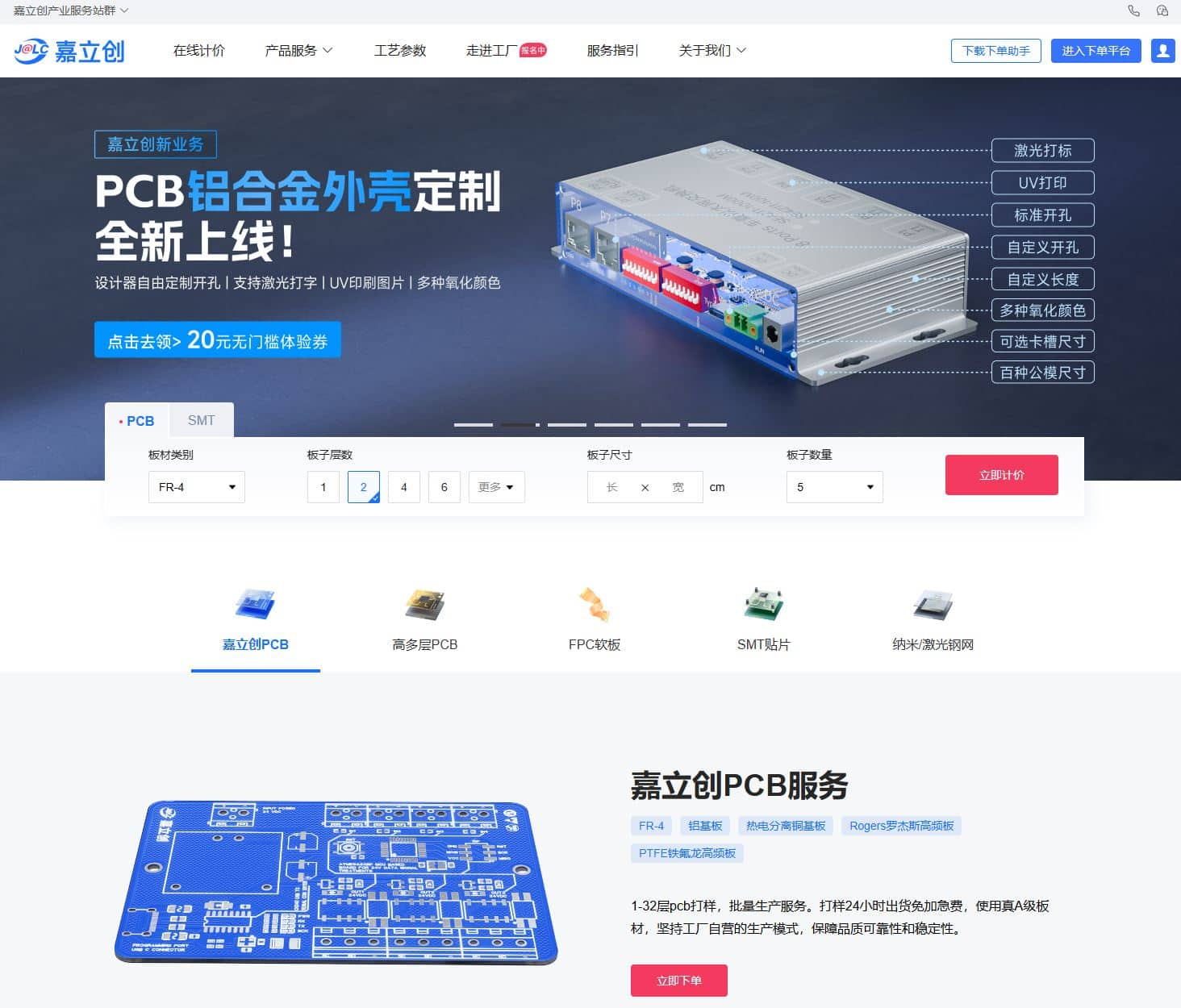
This is a online PCB-house and produce the PCB quickly. We can get the PCB product in 48 hours. We try to order the PCB production with our PCB design.
Parameters input
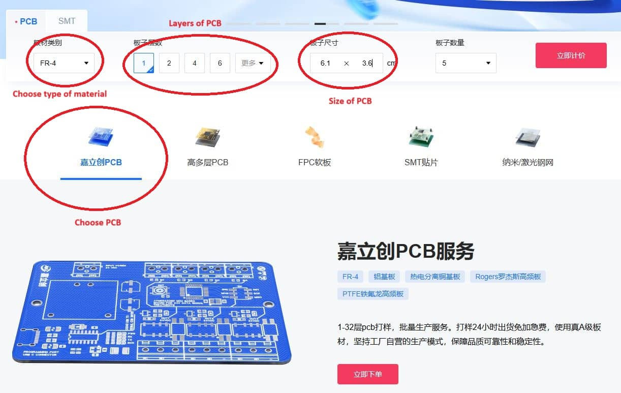
First, we input the basic parameters such as layers of PCB, type of material, size of PCB.
Then, a page with more input parameters come out. There're so many parameters...
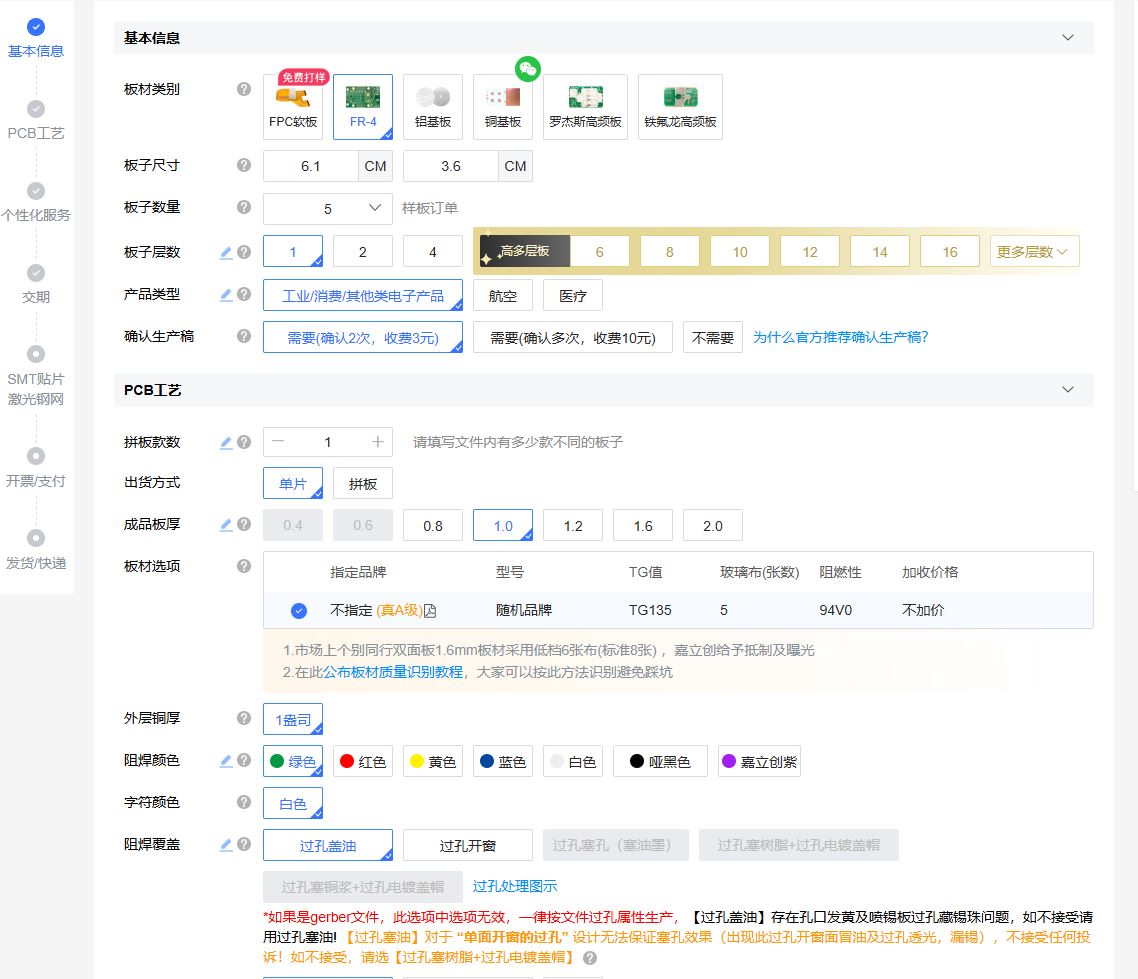
The basic parameters are:
- Type of Board : FR-4
- Size of PCB: 6.1cm * 3.6cm
- Layer of PCB: 1
- Thickness of PCB: 1.0mm
- Use of PCB: Consumer grade
- Type of Product: Economical Prodcut
Then, upload the gbr files in zip. Remember there're at least 5 files have to provided.
- F_Cu.gbr
- Edge_Cuts.gbr
- B_Mask.gbr
- F_Mask.gbr
- F_Silkscreen.gbr

After uploading the files, waiting for the technical checking by the system. If there's any technical question of the design file, the staff of jlc company will give us a phone call and provide the advices and help.
Confirm the draft
Before the production, system provides the draft-product comparsion to confirm the draft.
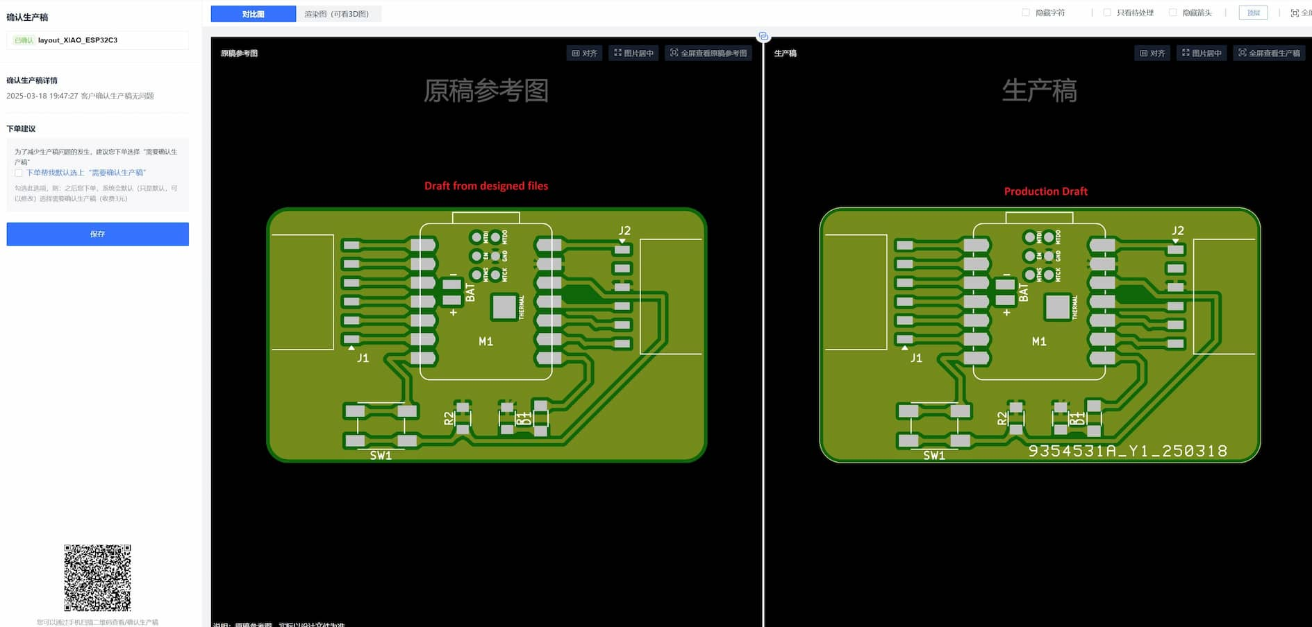
The draft on the left is generated from the designed files. The draft on the right is the production draft.
In the function, 3D view can be viewed.
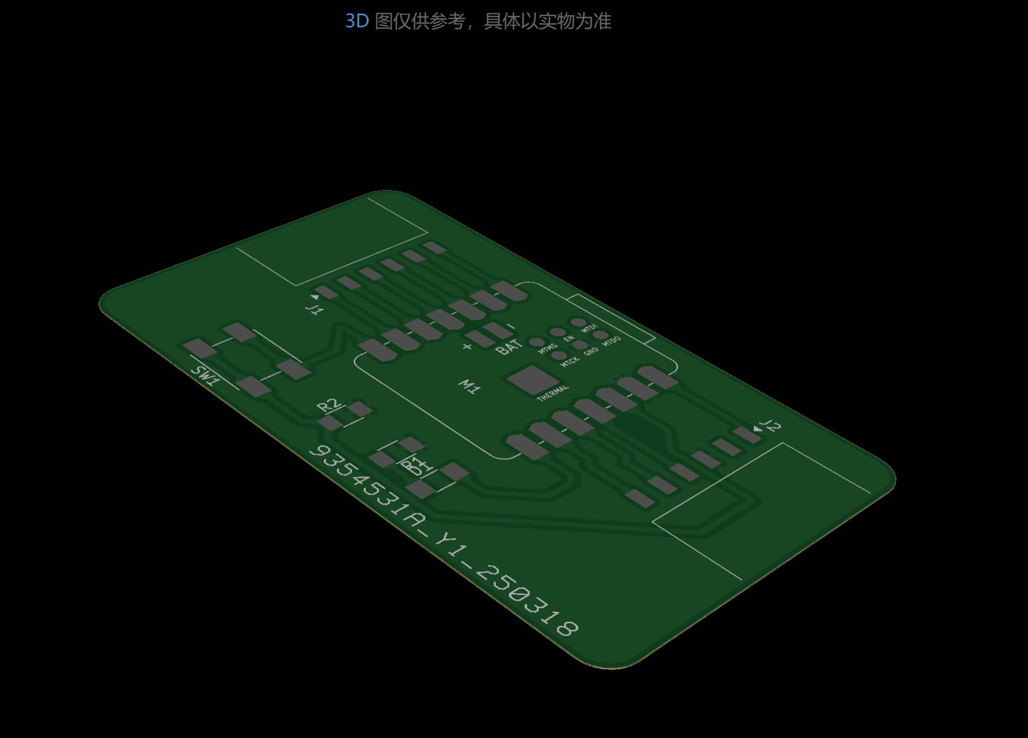
Waiting for production
I ordered 5 PCB production and spent RMB$33 (about USD$4.6) in 18th March, 2025.

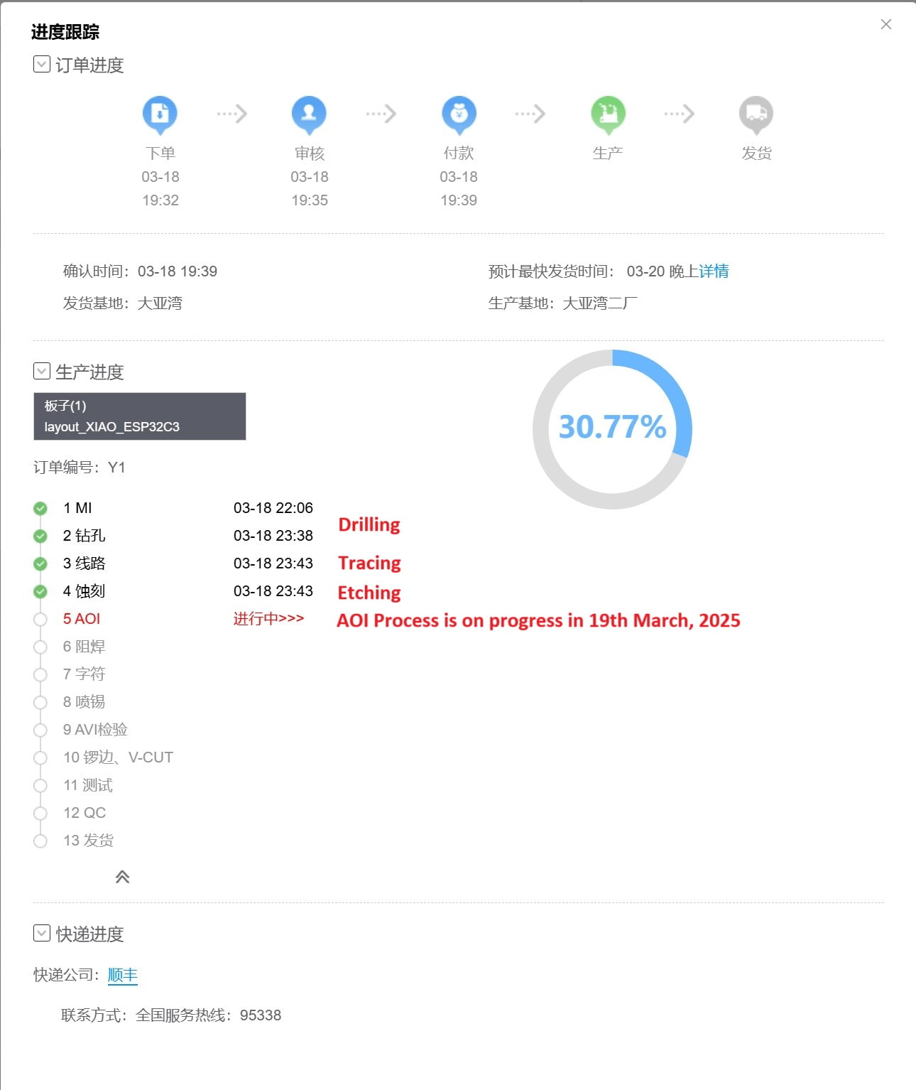
We can also track the progress of PCB production. In UTC+8 0:57 19th March, the etching process is finished. AOI (Automated Optical Inspection) process is on progress.
Receive the production
The PCB production is sent out at 3/20 night.
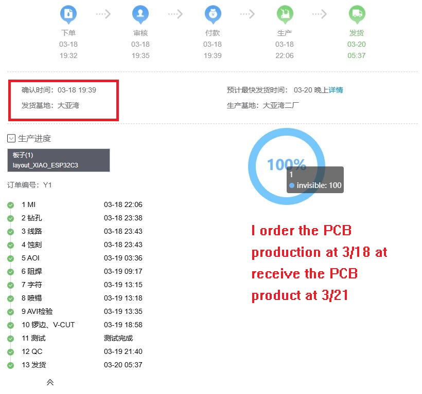
We receive a phone call about receiving the PCB production package at 3/21 afternoon.
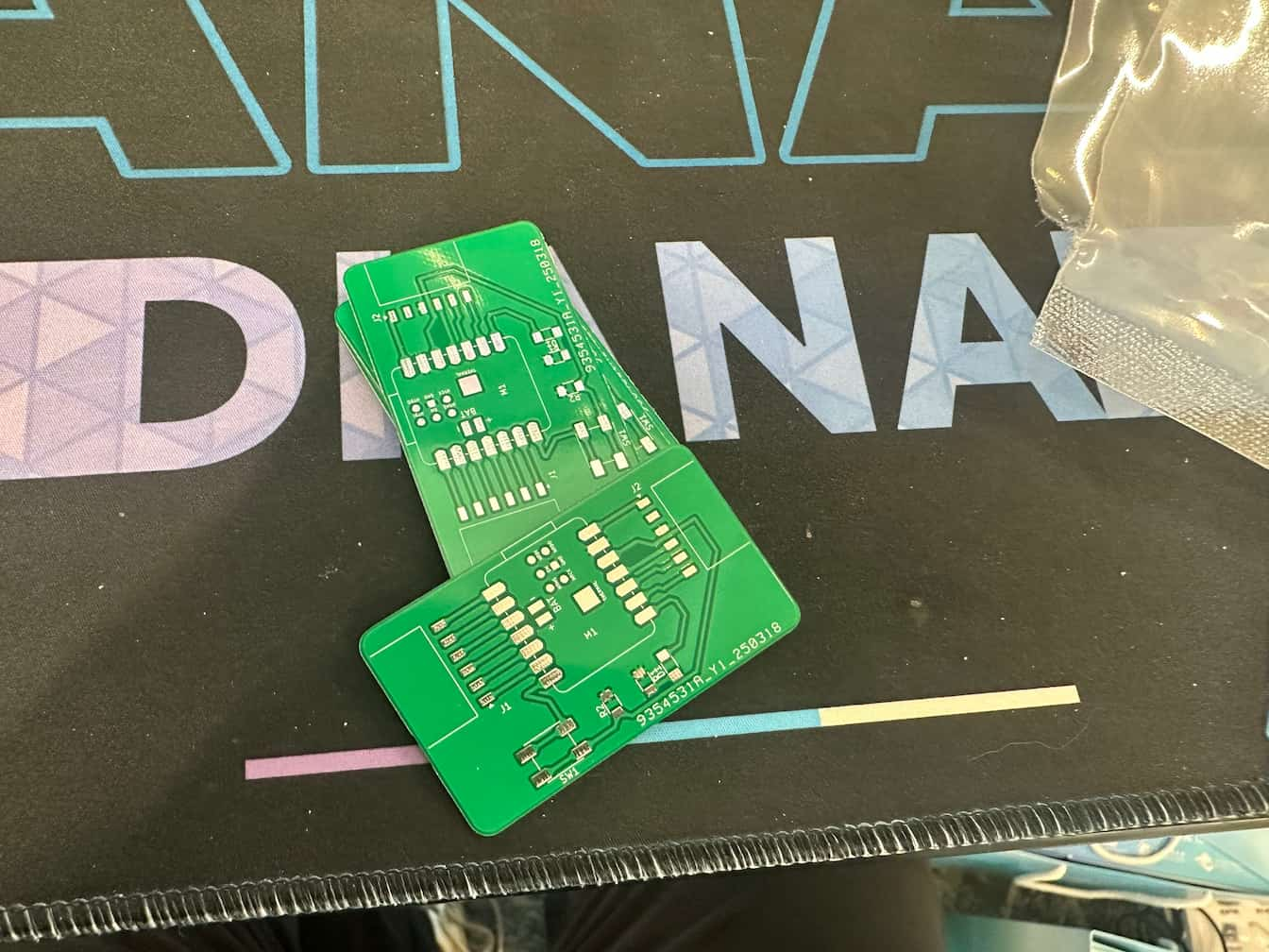
Then, we solder the components onto the PCB and it also works!!
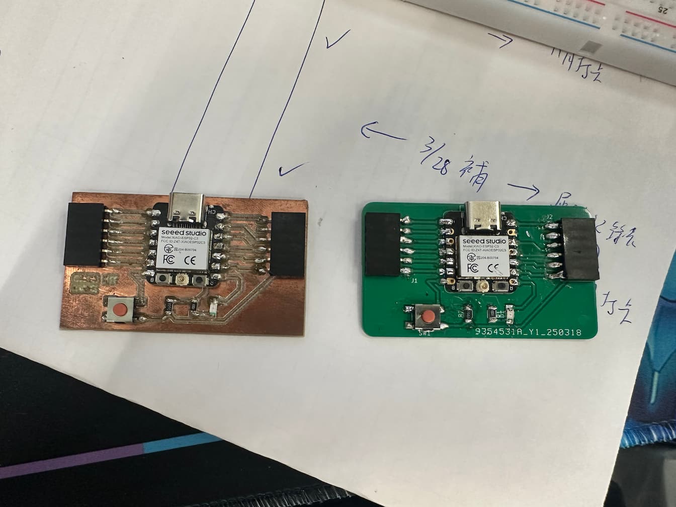
Here's the PCB made by milling and PCB by ordering online.
