Electronics Production
This week is dedicated to Electronic Production, focusing on understanding the materials, processes, and safety measures involved in producing electronic devices, particularly Printed Circuit Boards (PCBs). This includes learning about the materials required, machinery, software, safety protocols, and the various electronic components involved such as transistors, capacitors, inductors, microcontrollers,LED etc I studied all of these machines and the required tools to operate them, as well as the production of PCBs,Programming and documented all of this week's learning in the assignment.Task involved in this week is:
During this week, we completed a group assignment with objectives :
Understanding Printed Circuit Boards (PCBs)
Understanding the production of PCBs and associated machinery
Familiarizing myself with the materials used in PCB manufacturing
Exploring software utilized in PCB design
Studying electronic components such as transistors, capacitors, inductors, breadboards, jumper wires, connectors, and microcontrollers
Learning about soldering and desoldering processes
Exploring the origins and applications of software in PCB design.
This is all which we learn during week
PCB (Printed Circuit Board) fabrication:
This is the process of making the boards that electronic components are placed on. It's like the foundation of electronic devices.
There are differet process for PCB fabrication.
1. Etching:
Etching is a traditional method of creating designs on metal surfaces using strong acid or chemicals. It's commonly used in printmaking, along with engraving, and is still widely used today in technologies like making circuit boards. In pure etching, a metal plate is covered with a protective layer, then the artist scratches off this layer to expose the metal where they want lines. The plate is then dipped in acid, which bites into the metal where it's exposed, creating the design. After cleaning off the protective layer, ink is applied to the plate and wiped clean, leaving ink only in the etched lines. The plate is pressed onto paper, transferring the ink and creating a print. This process can be repeated many times before the plate wears out, and artists can add to or fix their designs by reapplying the protective layer and etching again. Etching is often combined with other techniques like engraving or aquatint to create more complex artworks.
Chemical required during etching process:
Acetic acid/White Vinegar (CH3COOH )/(CH3CO2H or C2H4O2)
Citric acid (C6H8O7)
Hydrochloric acid / Muriatic acid (HCl)
Hydrogen Peroxide (H2O2)
Sodium chloride (NaCl)
Copper sulfate (CuSO4)
2. Milling
PCB milling is like carving out shapes from a flat piece of material to make a circuit board. Instead of cutting with a knife, it uses a special machine to remove copper in specific areas based on a digital plan. This plan tells the machine where to remove copper to create the electrical paths and structures needed for the circuit board.
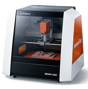
We used Roland Monofab SRM-20 machine for milling.
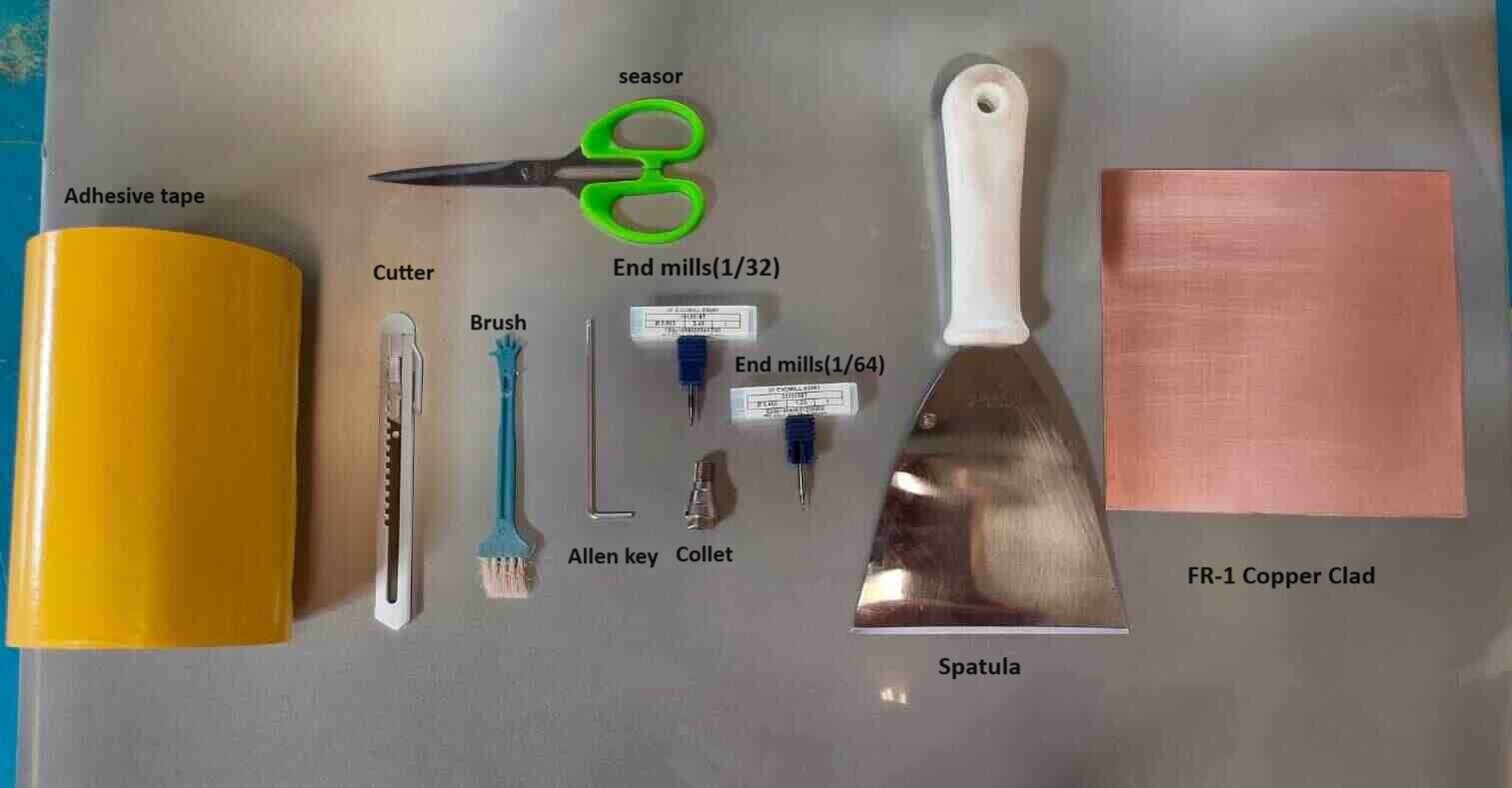
Material and tools required for milling are:
FR-1 Copper Clad
Adhesive tape
Allen Key
End mills(1/64,1/32)
Spatula
Dusting brush
Scruber
vaccum cleaner
seasor
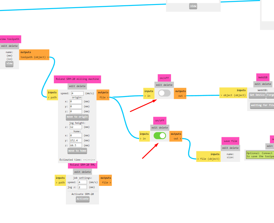
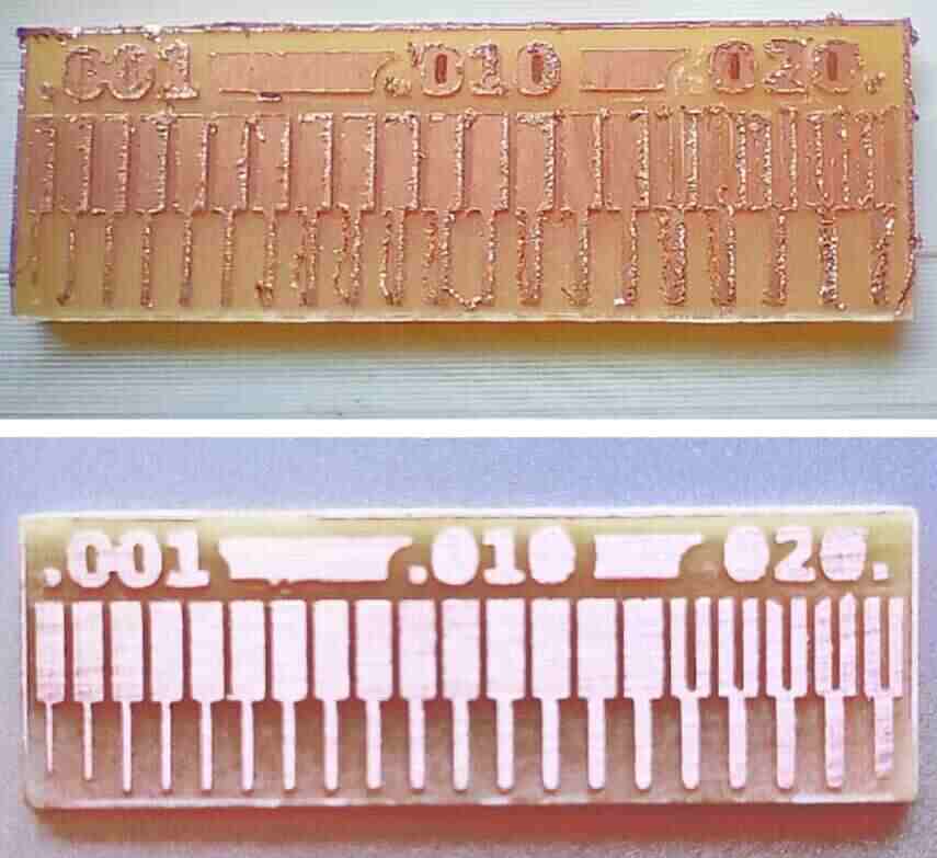
This week has been dedicated to electronic production, with a specific focus on understanding the precision and capabilities of the milling machine SRM-20. Testing the accuracy of this machine is crucial as it allows us to establish precise production specifications, ensuring the quality of our output.
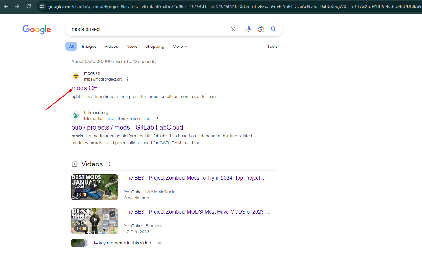
To begin, we obtained a linetest PNG image from a reliable source online. Using mods ce, we made necessary adjustments to parameters such as tool diameter, origin coordinates, and end mill specifications.
These adjustments are critical for aligning the machine's settings with our production requirements. Subsequently, we converted the PNG file to RML format, which serves as the input for the milling machine. Through this process, our group successfully characterized the design rules for our production process, laying the groundwork for efficient and accurate PCB milling.
Stepwise Procesure for PCB fabrication:
1. Test Print Production:
First we have start with production of test print,Begin by downloading the trace and cut file in PNG format from the Mods CE website. Import the downloaded file into our production machine.
2. Program Selection and Configuration:
Visit the "Mods CE" website for designing PCBs. Right-clicking anywhere on the site gives you four options:
1.Modules
2.Programs
3.Edit
4.Options
In programs again for options:
Open program for file
Open program
Save program to file
Save HTML page
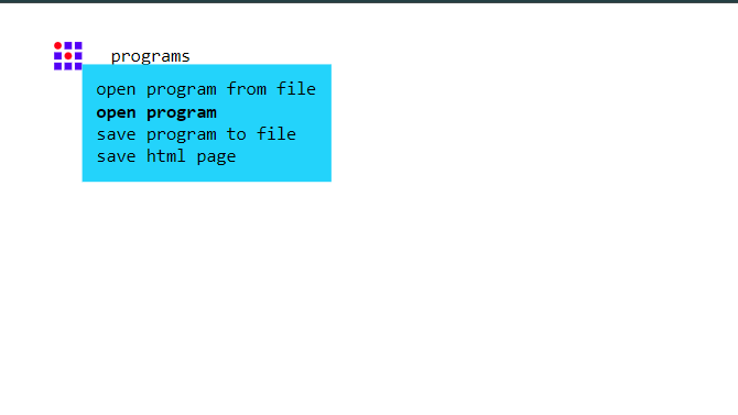
We choose the "Open Program" option and select the SRM-20 mill machine, specifying "mill 2D PCB."
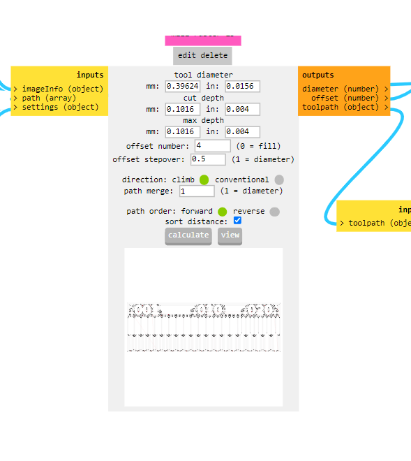
Import the downloaded file into the program.Set the PCB defaults and choose a 1/64 end mill for tracing.
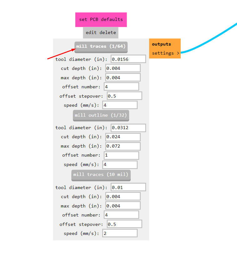
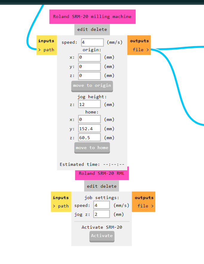
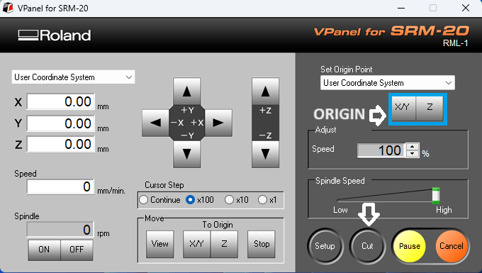
Configure parameters such as x, y, z distances from origin, speed, and job height for roland SRM machine.we take job height at z axis is 12mm.
3. File Saving and Conversion:
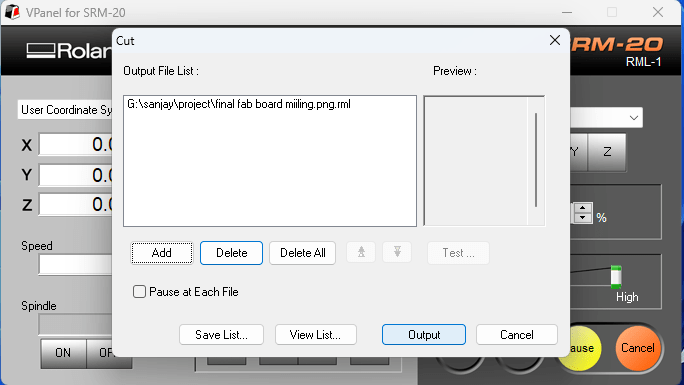
Disable the WebUSB option and enable the save file option.Save the file, which will generate an RML file necessary for the PCB milling machine.as we saved our file all selection goes to mill raster 2D then simply calculate it. it gives us RML file which is input for our PCB milling machine.
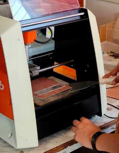
4.Milling PCB by connecting the milling machine with pc.
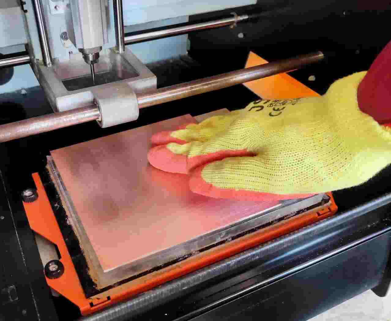
In our lab vigyan ashram we have Roland Monofab PCB milling machine.we have Cleaned the Roland Monofab PCB milling machine thoroughly before use and placed the copper clad on machine bed.
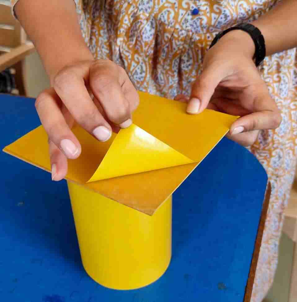
First, apply double-sided adhesive tape carefully to the backside of the copper clad, ensuring no bubbles and uniform application.
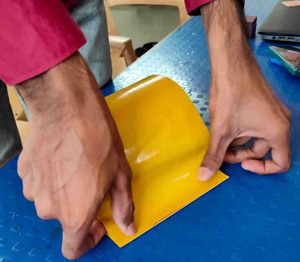
Then, use a cutter to trim any excess adhesive and clean the bed.
Next, place the substrate on the table and utilize the VPanel controller to position the machine table for proper substrate placement. Ensure the substrate is uniformly positioned across the table surface, maintaining a consistent level throughout. Finally, mark the Zero position on the XY axis and, if feasible, on the substrate itself for efficient utilization and minimal waste.
5. Machining PCB
Then we go to the production part for that we connected the PCB mill machine with our Computer. We have opened v panel software for our machine.As we have already selected end mill into mods ce software. Here is important to set the machine tool and then we have to set the head and machine bed position according to space on pcb. Then we have to set end mill x,y,and z position and then with gravity we have to touch the end mill to Copper clad then the machine is ready for printing.
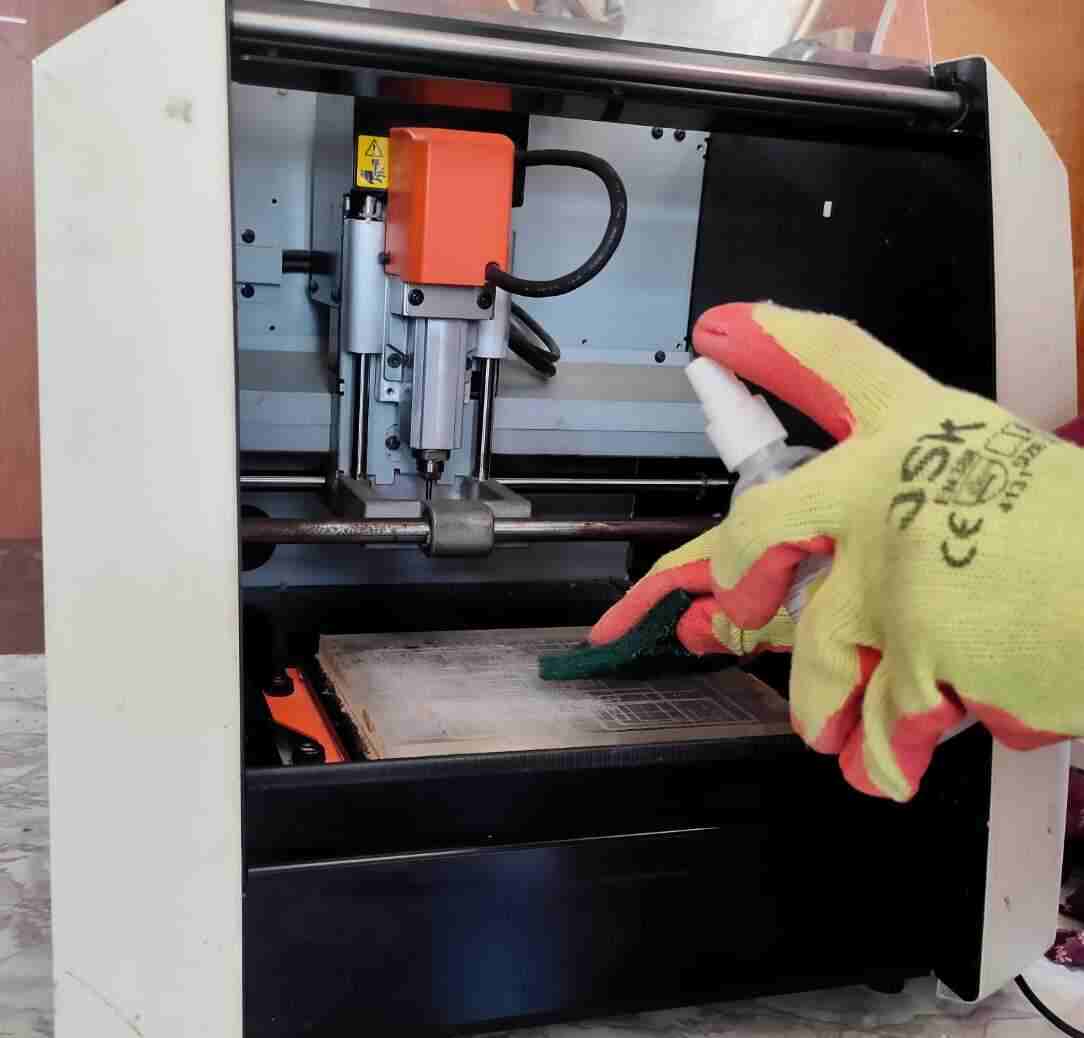
here most imortant is to cut the previous file and select new one.we have first selected downloaded trace file and origine xy and z then click on output button for start the milling process.
After completing the milling , we cleaned the machine and our precision and accuracy test is done.This is our trace print.
Conclusion / Keylearnings:
In summary, This week we've learned a lot about making electronic stuff, especially Printed Circuit Boards (PCBs). We also learnt about how PCBs are made, the machines used, the materials needed, and the software for designing them.
We have also studied the different parts like transistors, capacitors, and microcontrollers, as well as how to solder them together.
One big focus was on testing a milling machine called SRM-20 to make sure about its accuracy and precision. All this knowledge helps us make perfect PCB milling in terms of how to set the parameter speed,depth,tool selection,origin. So that we understood our machine mill capability and accuracy.our machine can trace upto third last acuurately.