8. Electronics Design
The primary goal for this week is to utilize an Electronic Design Automation (EDA) tool to design, produce, and test a development board. The board must interface and communicate effectively with an embedded microcontroller, ensuring optimal operation and seamless integration into the final electronic system.
EDA stands for Electronic Design Automation, which refers to a set of software tools used by hardware design engineers to automate tasks such as logic synthesis, signal routing, functional verification, and PCB (Printed Circuit Board) design. The use of EDA is critical in the semiconductor and electronics industry as it streamlines the design process and improves the quality of electronic products.
In my experience, I have used KiCAD, an open-source software widely recognized in the field of electronic circuit and PCB design. This program is appreciated by engineering and design professionals for its ability to efficiently produce schematics, design PCBs, and verify electronic designs. It offers several advantages, such as being free of charge, having an active community that supports it, being customizable, and being compatible with multiple platforms.

Image taken for KiCAD Official Web Page
Research
The group assignment for this week can be accessed via the link here.
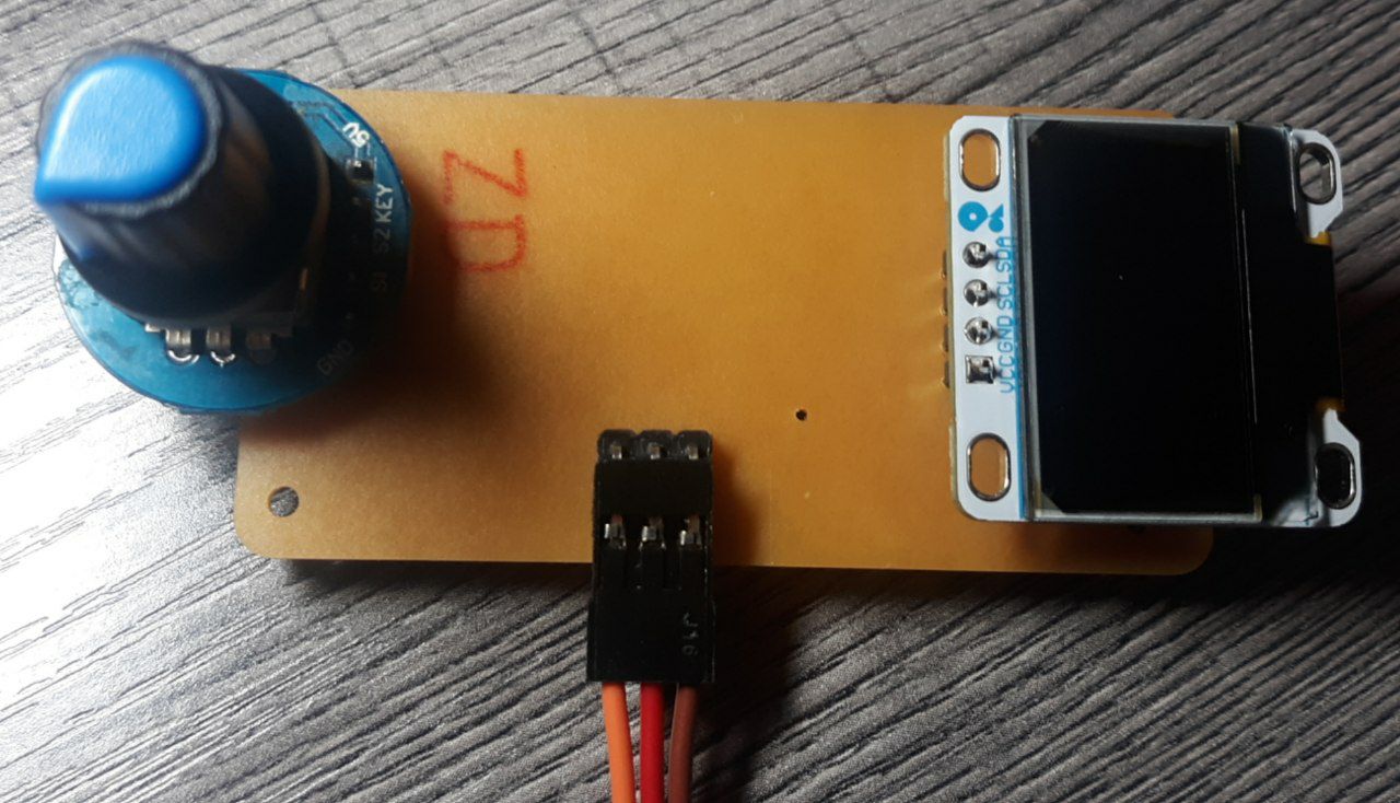
This week, I tasked myself with designing a PCB that could accommodate the circuit I created in week 6 without requiring wiring or breadboards.
The following tutorial about using KiCAD, is based on other you can find here.
To get started, you need to download and install KiCAD from the official website. Versions are available for Windows, Linux, Mac, and even Docker.
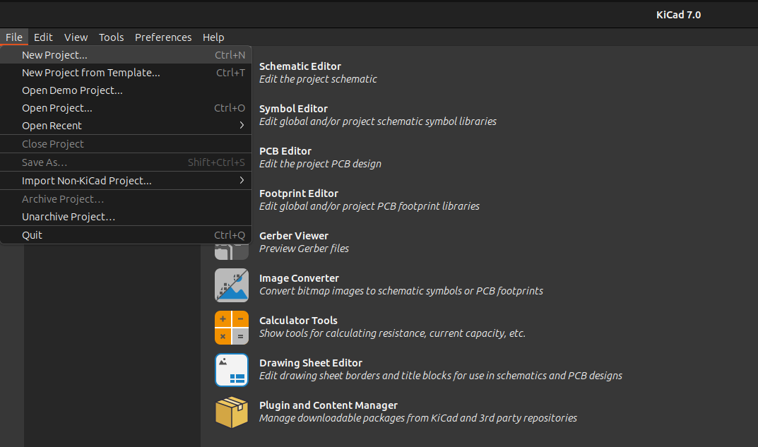
When we launch KiCad, we will be greeted by the main KiCad window. From here, we aim to start a new project. This can be done by clicking File -> New Project or pressing Ctrl+N.
To begin, a new window will open where you can select a name for the project (it is recommended to choose a name that aligns with the project's purpose to avoid confusion) and a folder to create it in:
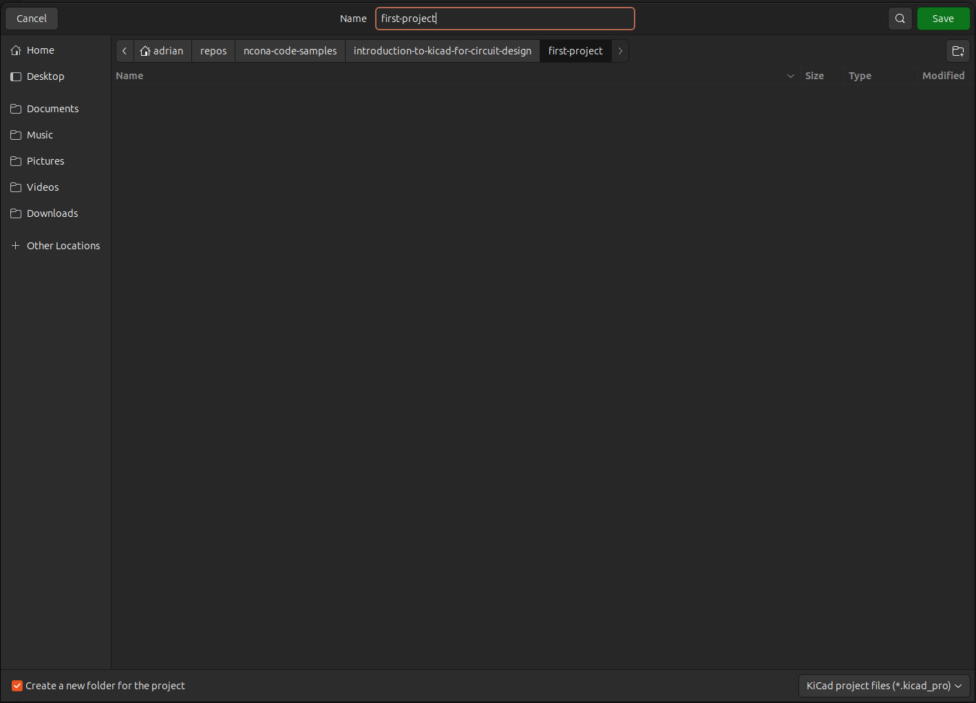
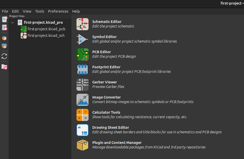
A folder with the same name as the project will be created, and the project files will appear on the left side of the main window.
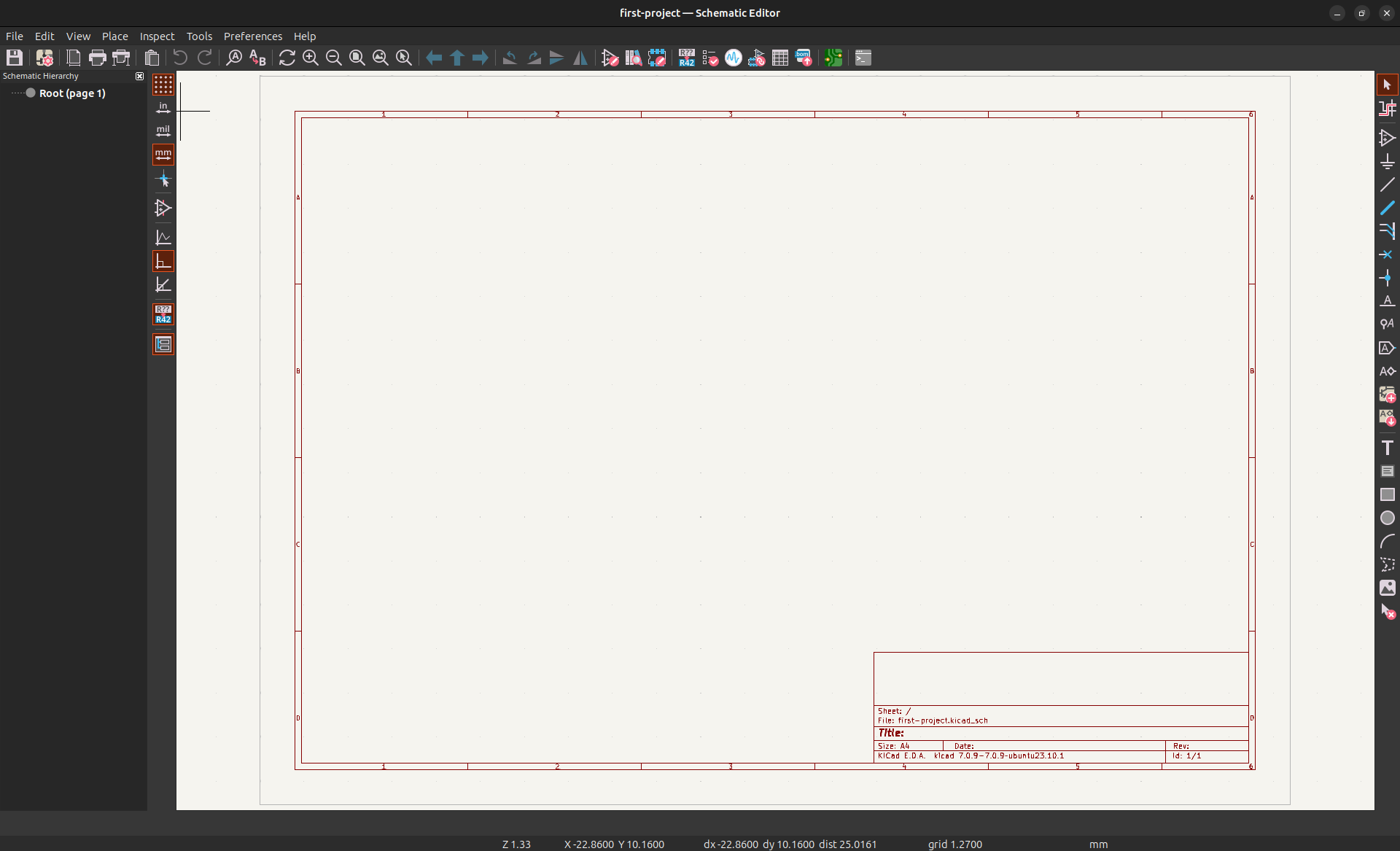
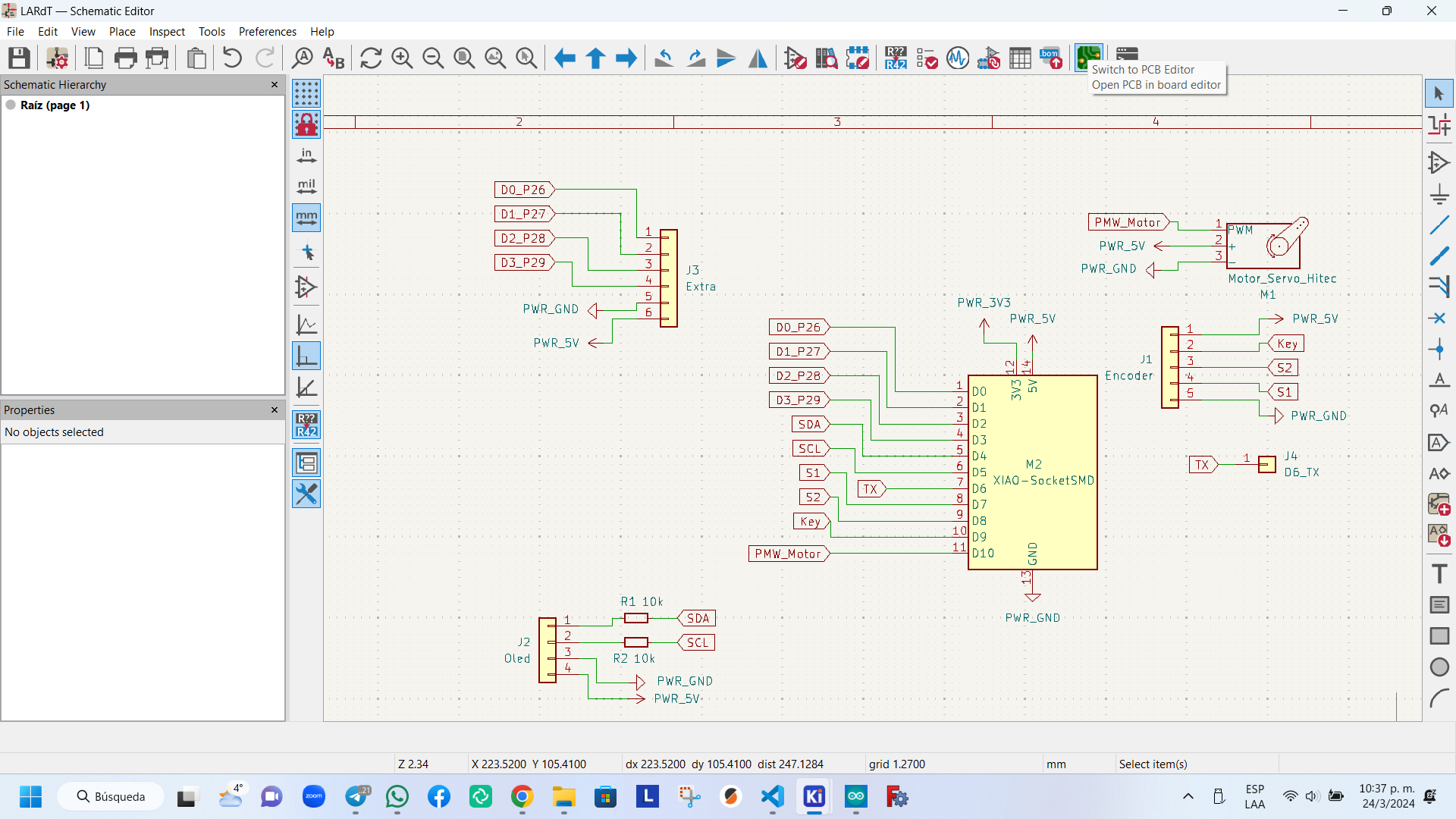
To begin a project, it is recommended to first design the schematic in KiCad. A schematic is a document that displays the logical structure of an electronic circuit, including its components and their connections using symbols and lines to represent electrical connections. The schematic in KiCad is a crucial element of the electronic circuit design process. It serves as a reference for the physical layout of the components on the PCB. To begin, we need to click on the Schematic Editor icon on the right:
The schematic editor window will open upon taking this action.
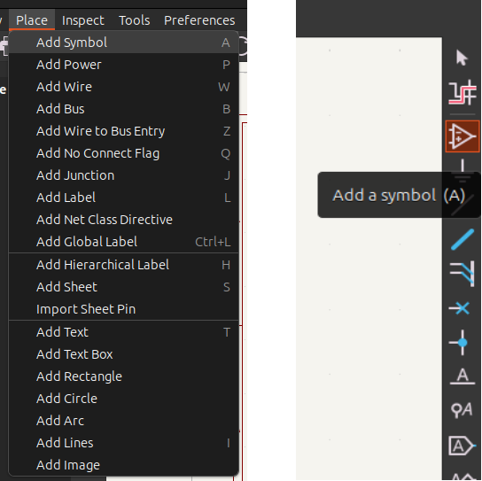
In the schematic editor, components can be added to the project by inserting their electrical symbols. This can be done in three ways: opening the symbol selection window by clicking on Place -> Add symbol, clicking on the add symbol icon in the toolbox on the right, or pressing the A key.
The Symbol Chooser allows you to add symbols for the components needed in the project. You can search the default list of installed KiCAD components or install additional components as needed. Additionally, you can add the component's footprint for use in the PCB design.
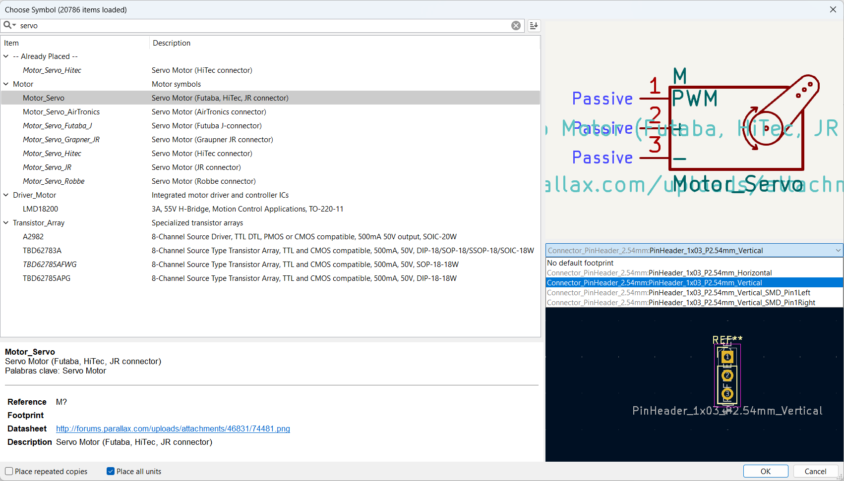
The Symbol Chooser allows you to add symbols for the components needed in the project. You can search the default list of installed KiCAD components or install additional components as needed. Additionally, you can add the component's footprint for use in the PCB design.
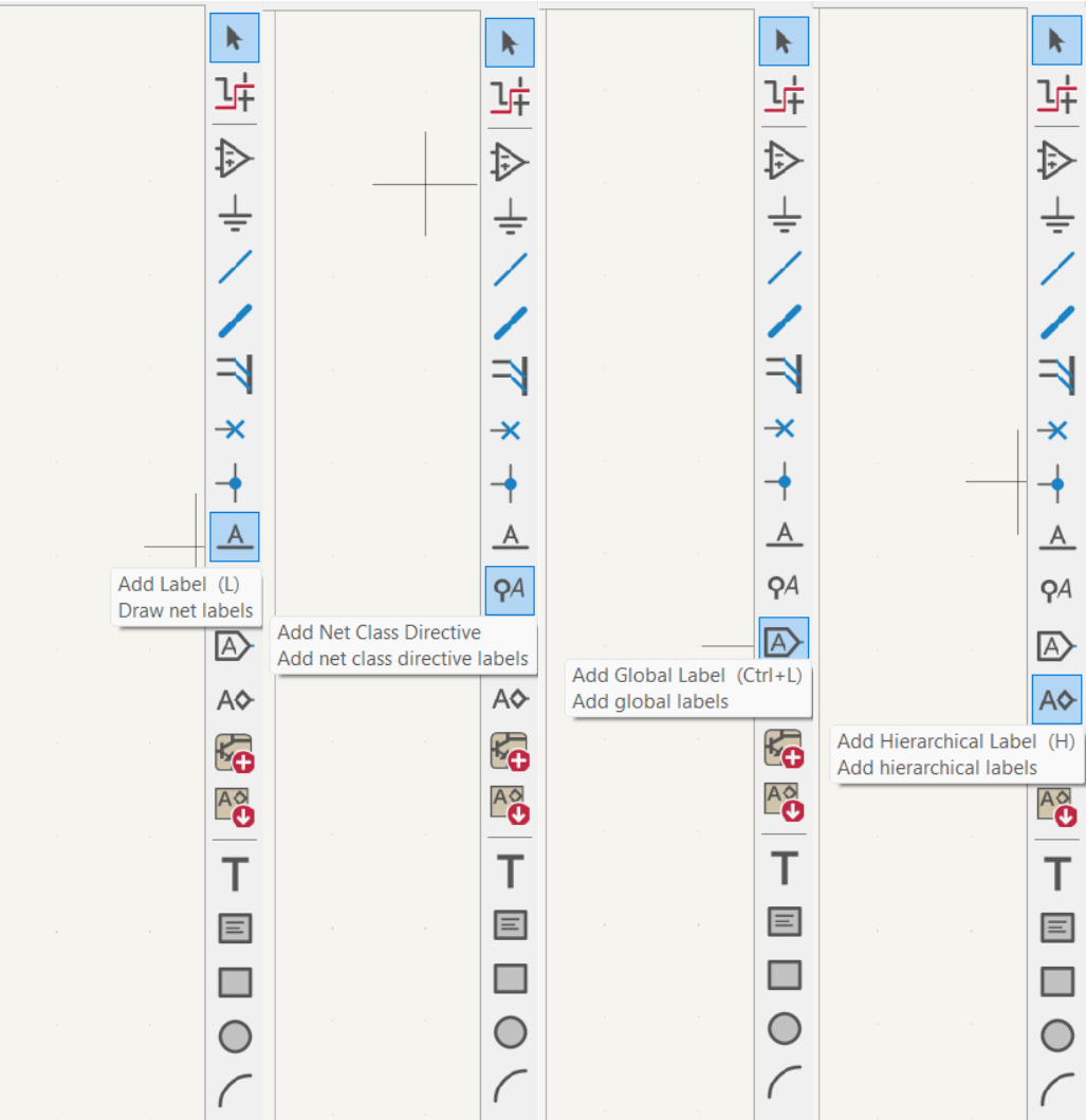
KiCAD has four types of labels: simple, global, network class directives, and hierarchical. Simple labels, simply called labels, are used to name individual components or connections in a schematic. They uniquely identify a particular component or connection within the design. Global labels identify a connection that spans the entire project, allowing multiple elements on different sheets of the schematic to be connected. Global tags are utilized to establish connections that span the entire design, regardless of the physical location of the elements. Network class directives are configurations that apply to a specific group of electrical networks with similar characteristics, such as track width, spacing, and design constraints. They allow for the definition of specific rules for a set of electrical networks instead of configuring them individually. Hierarchical labels are utilized in hierarchical design to connect different sheets of the schematic and establish communication between different hierarchy levels. This allows for the definition of ports in upper and lower sheets to facilitate interconnection and signal transmission. These labels can be added using the toolbox on the right.
Once the schematic design has been completed, the PCB is designed based on the electrical design made. To do this, open the PCB editor in the toolbox located at the top.
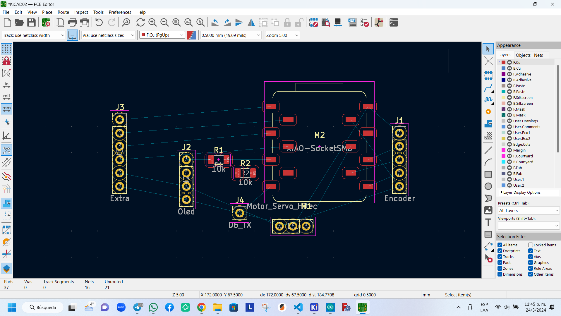
In the PCB editor, the footprint of the electrical components are updated based on the schematic design.
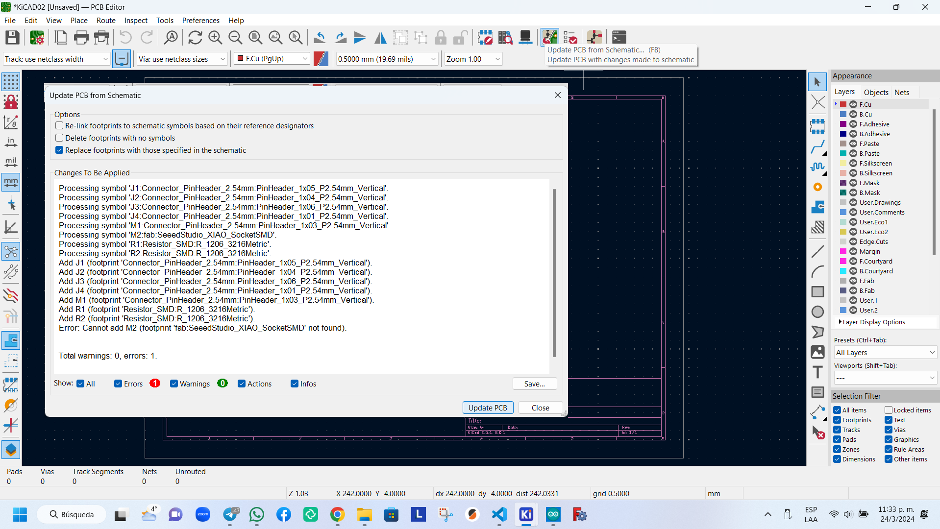
By adding the footprints you can see the electrical connections that exist in the components and that are derived from those established in the schematic editor.
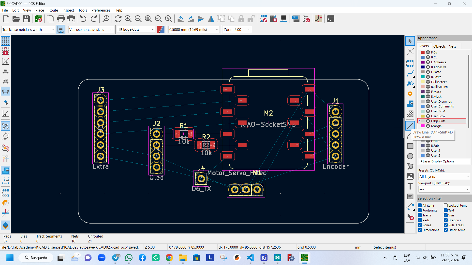
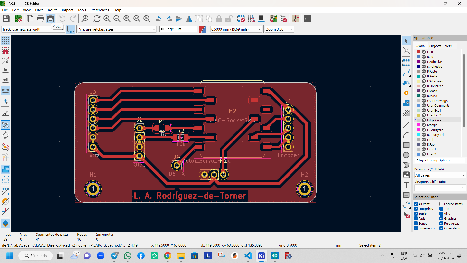
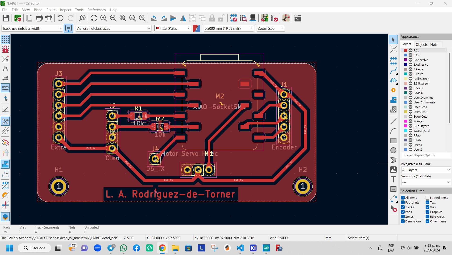
To add an edge to the plate, select the Edge.Cuts layer and trace it. The most advisable thing is to use the line and circle arc tracer, although it is also possible to make more complex drawings, and even import them in .dxf format.
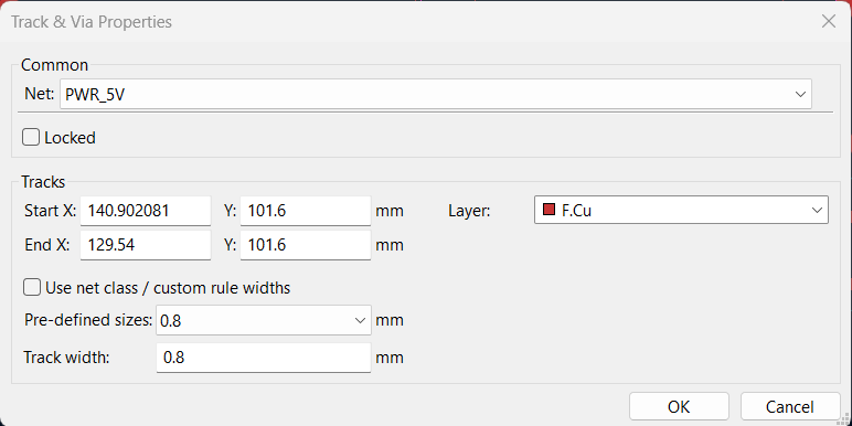
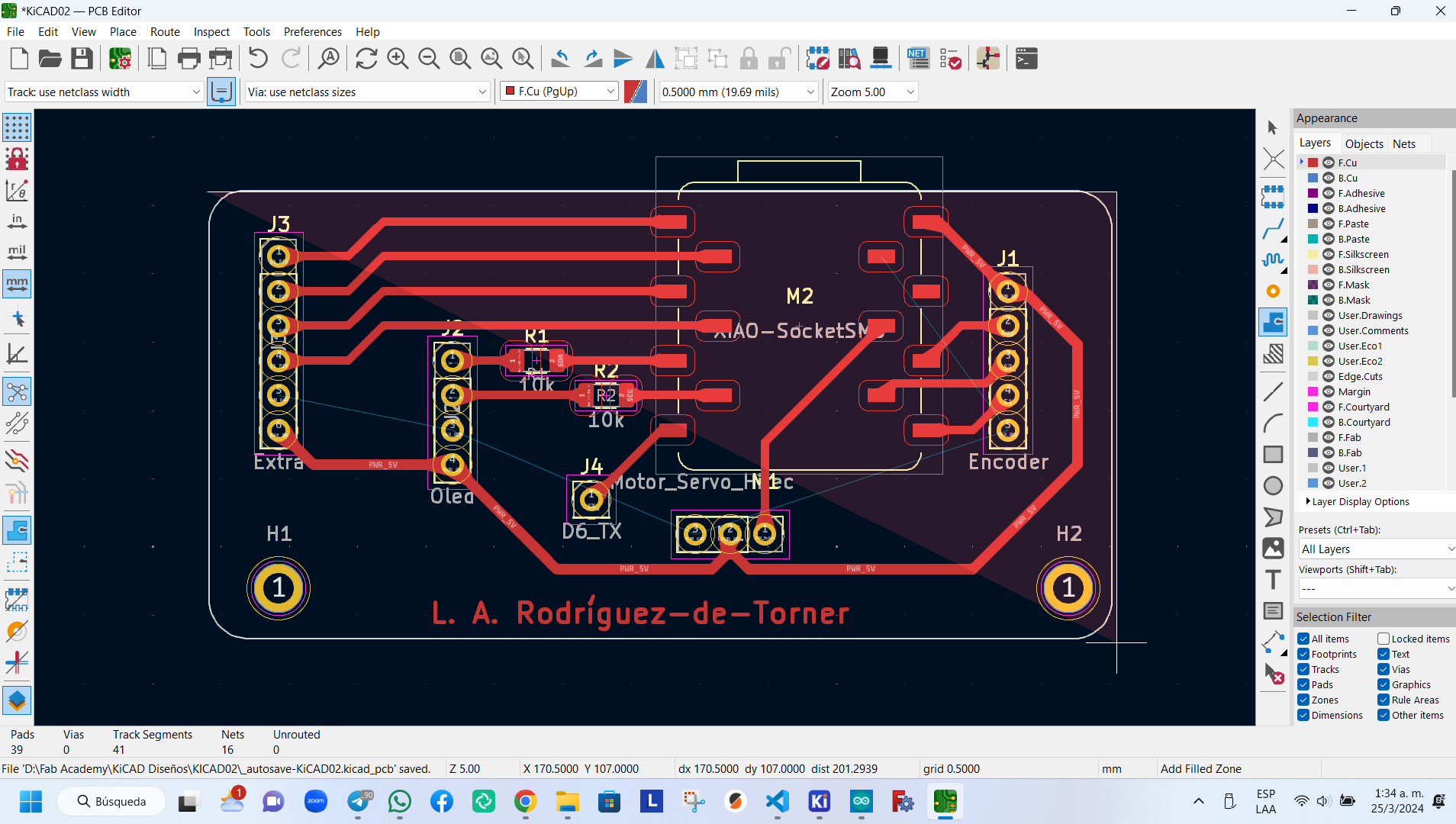
Subsequently, the tracks that will connect to the terminals must be laid out, except for the ground connection, which has another way of doing it. To lay out the tracks, it is always recommended that the connection angles be between 0° and 60° (or between 120° and 180°), avoiding angles close to 90° at all costs. This is because when milling you should try to ensure that the milling machine makes smooth movements. To trace the tracks, select the F.Cu layer, which corresponds to the upper copper side of the PCB. Click on the track tracing button (or press the X key) to start tracing the tracks. If the B.Cu layer is used in the design, it corresponds to the lower copper side of the PCB.
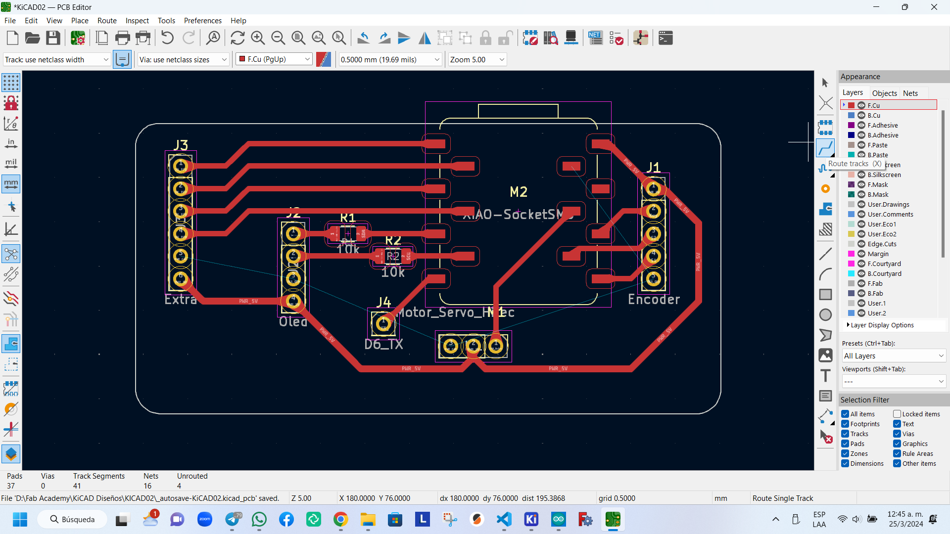
The properties of tracks can be modified by double-clicking on them. For power tracks (Vcc) a minimum width of 0.8 mm is recommended and for information tracks a minimum width of 0.6 mm.
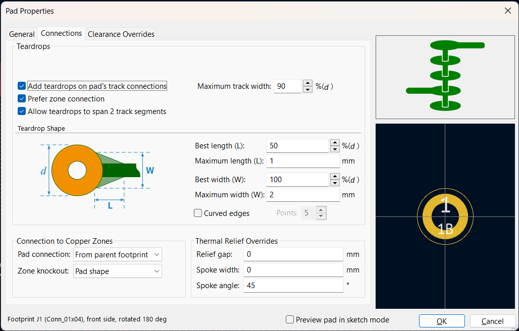
It is advisable to add teardrops to the plate pads, as these serve to facilitate a smooth transition between a copper track and a pad. This improves the distribution of current flow and reduces the concentration of mechanical stresses in that area. In contrast, a direct right-angle junction is more susceptible to issues such as breakage or tearing during the manufacturing process and use. To incorporate teardrops into the plate pads, navigate to the Connections section of the Pad Properties window and input the recommended values for the desired design.
It is possible to customize the board by adding fixing holes, texts and shapes, using the toolbox on the right of the PCB editor.
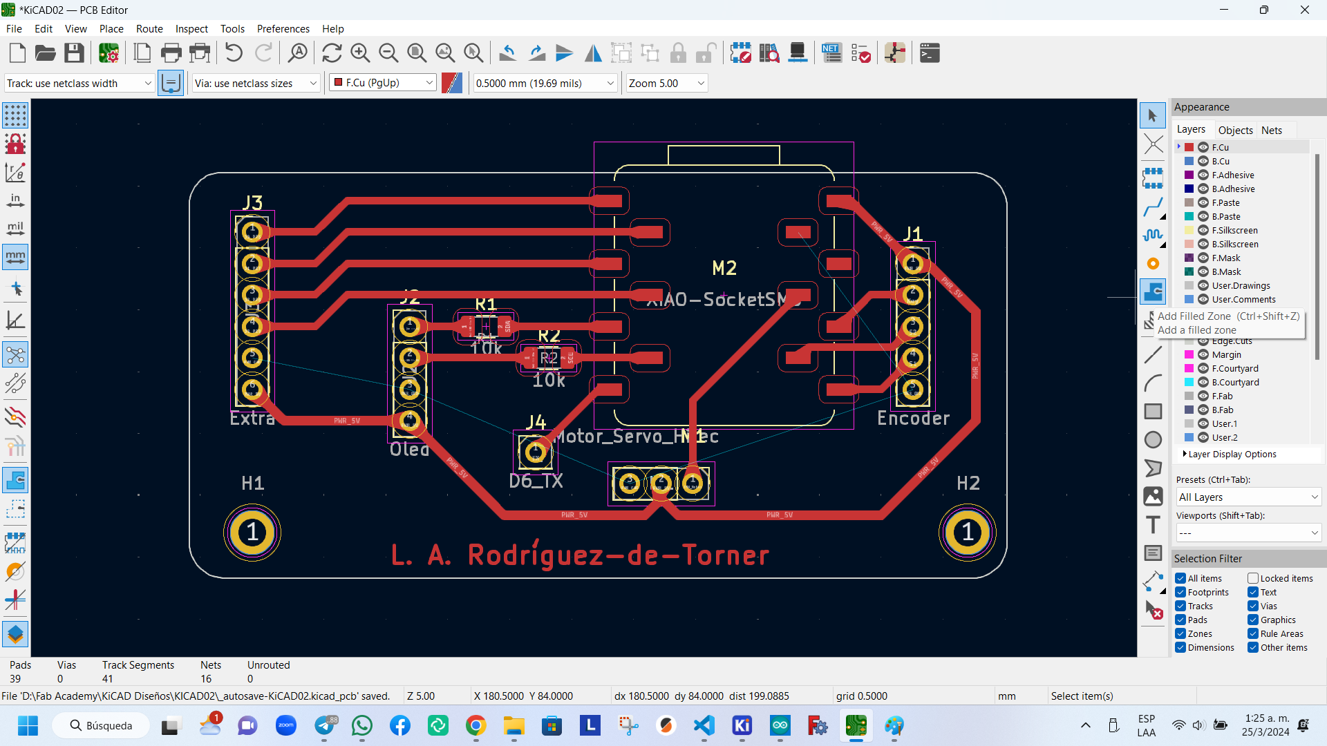
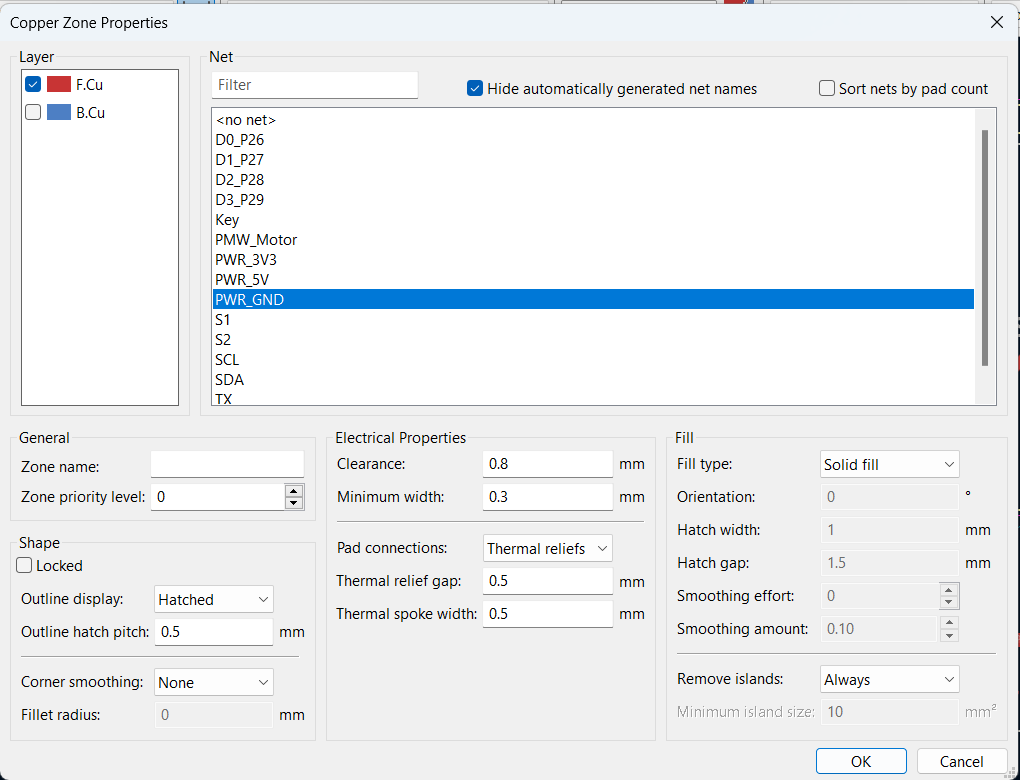
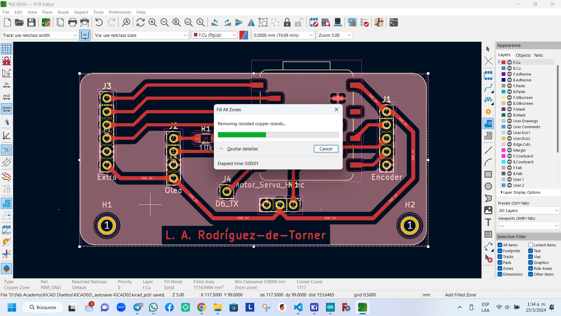
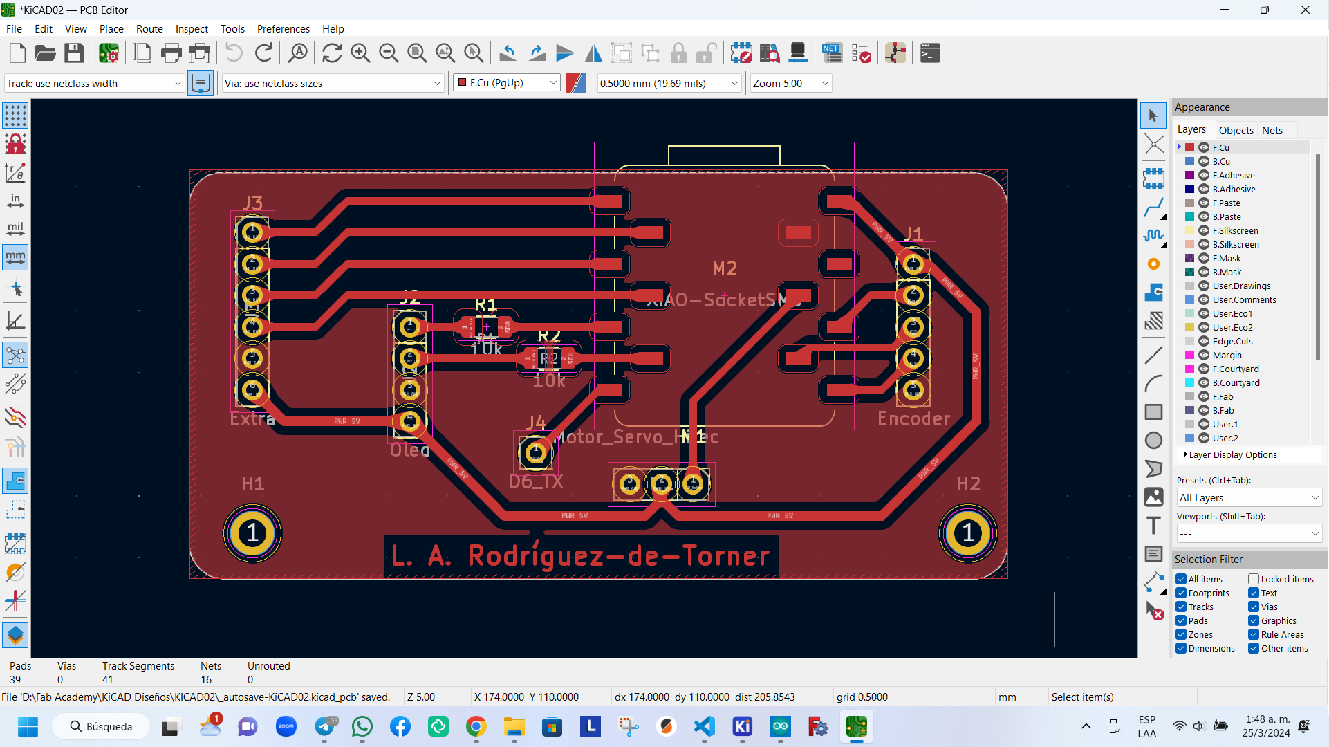
To create the ground plane, select 'Add Fill Area' from the toolbox in the PCB editor (or press Ctrl+Shift+Z) and choose the starting point for the plane. The process opens a new window. To select the layer to use (F.Cu), choose the plane to work on (PWR_GND, which in this case corresponds to ground), set the clearance (distance between the ground plane and any other connection that does not belong to the ground plane, recommended to be at least 0.8 mm), and choose the type of fill (recommended to be solid), among other options. Afterwards, press OK and continue drawing the border. When the figure is closed, press the B key to show the ground plane.
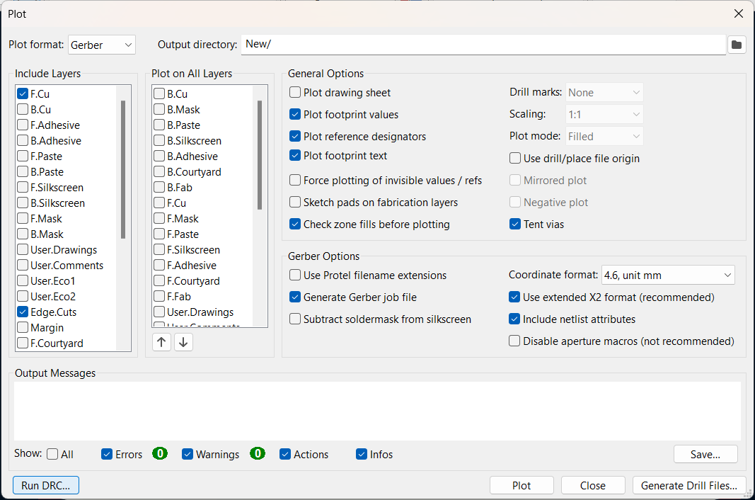
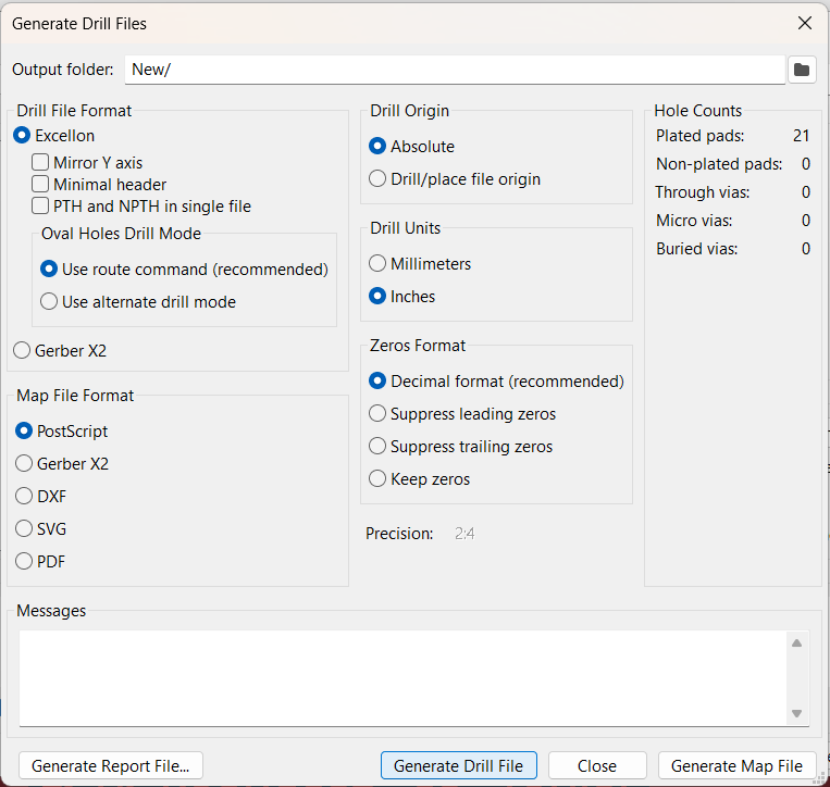
To generate the print files for the CNC to mill the PCB, click on the Plot button located in the top toolbox of the PCB editor.
This action will open a new window titled 'Plot'.
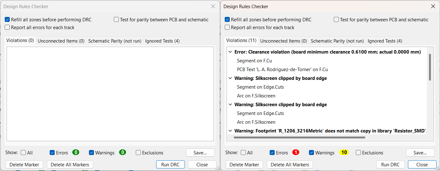
To check for errors in the design, click on the 'Run DCR' button. To check for errors in the design, click on the 'Run DCR' button. This will open the Design Rules Checker window, where any errors or warnings will be displayed. Errors will be marked with red arrows and warnings with yellow arrows on the board.
To generate the drill files, click on the 'Generate Drill Files' button in the Plot window. This will open a window with the same name. From there, select the PostScript option in the Map File Format and choose the appropriate drill units for your CNC. Leave the rest of the parameters as default. Finally, select the location of the files and click on 'Generate Drill Files'.
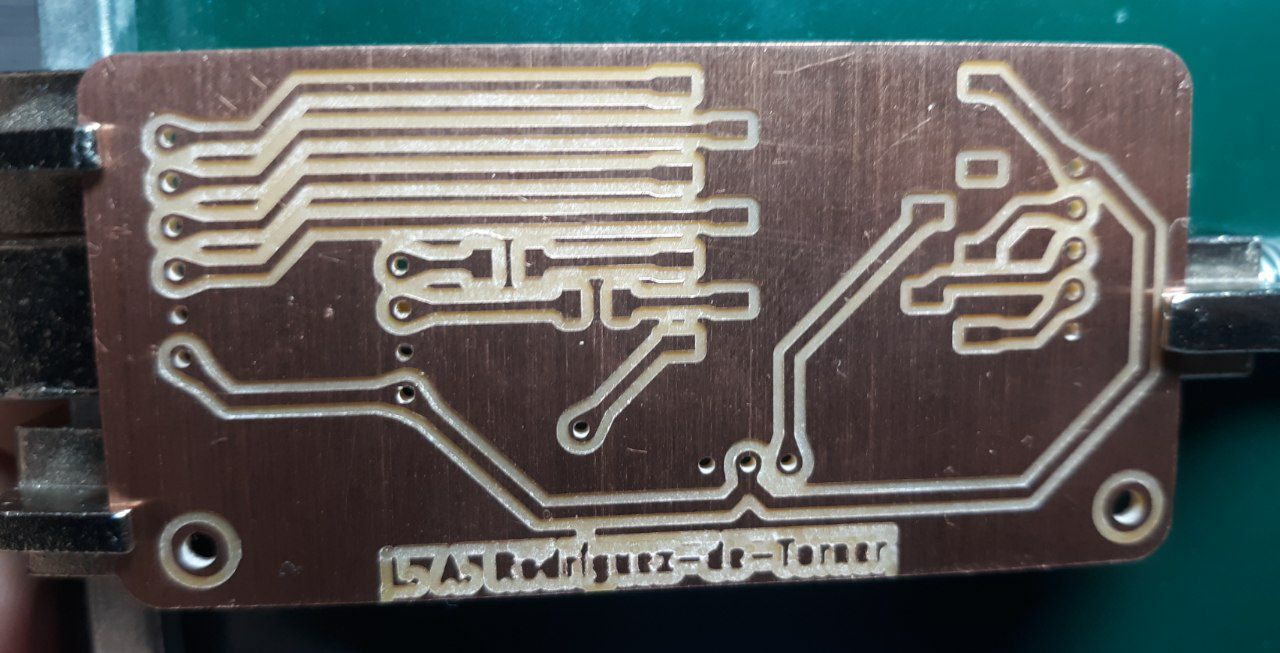
The plate produced by the Bantam milling machine, as described in week 4, is visible here.
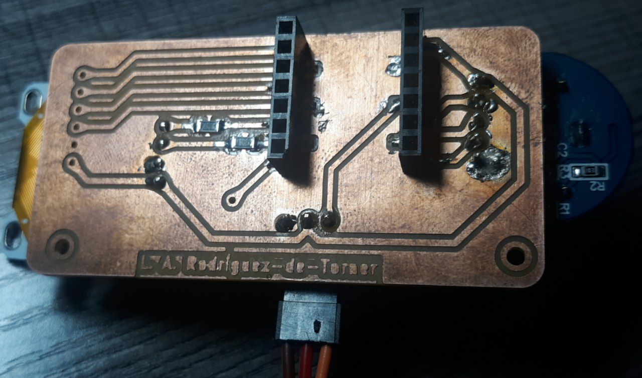
The motor speed was controlled using the code from week 6, which was modified from the original code found here.
#include "RotaryEncoder.h"
RotaryEncoder encoder(1, 2);  // (DT, CLK)

#include "Servo.h"
Servo servo;

#define STEPS  10
#define POSMIN 0
#define POSMAX 180

int lastPos, newPos;

void setup(){
  servo.attach(3);
  Serial.begin(9600);
  encoder.setPosition(10 / STEPS);
}

void loop() {
  encoder.tick();
  newPos = encoder.getPosition() * STEPS;

  if (newPos < POSMIN) {
    encoder.setPosition(POSMIN / STEPS);
    newPos = POSMIN;
  }

  else if (newPos > POSMAX) {
    encoder.setPosition(POSMAX / STEPS);
    newPos = POSMAX;
  }

  if (lastPos != newPos) {
    Serial.println(newPos);
    lastPos = newPos;
  }

  servo.write(lastPos);

}
The files necessary for the fabrication of the plate may be downloaded by clicking the button below.