4. Electronic Production
The process of producing electronic boards for microcontrollers, such as Arduino, Raspberry Pi, ESP32, Blue Pill, Black Pill and others, involves multiple stages. Firstly, the board's schematic is designed to define the necessary connections and components for the microcontroller's operation. Next, the board's layout is designed, with components strategically placed to ensure proper operation and minimize electromagnetic interference.
Once the design is finished, the board prototype is manufactured for functional testing and corrections, if necessary. This is followed by mass production, which typically involves techniques such as silkscreen printing, surface mount assembly of components (SMD), and reflow soldering. These electronic boards are highly specialized and require strict quality control throughout the manufacturing process to ensure proper operation.
The production of electronic boards for microcontrollers has evolved over time, enabling the manufacture of smaller, more efficient, and more powerful devices. This advancement has contributed to the development of innovative applications in fields such as robotics, home automation, industrial automation, and the Internet of Things.
Research
This week, we will focus on the production processes of electronic boards for microprocessors. Understanding each phase of manufacturing, from material selection to final assembly, is essential to ensure product efficiency and quality.
This week's group assignment involves characterizing the design rules for your internal printed circuit board production process and submitting a printed circuit board to a board manufacturer. The results are available here.
This week's individual assignments consist of three parts: one mandatory and two optional. The mandatory assignment, described below, involves fabricating and testing a microcontroller development board using a design provided by Quentorres Project.
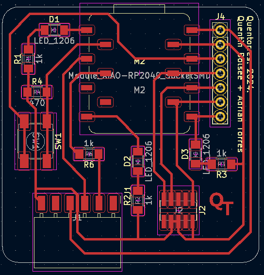
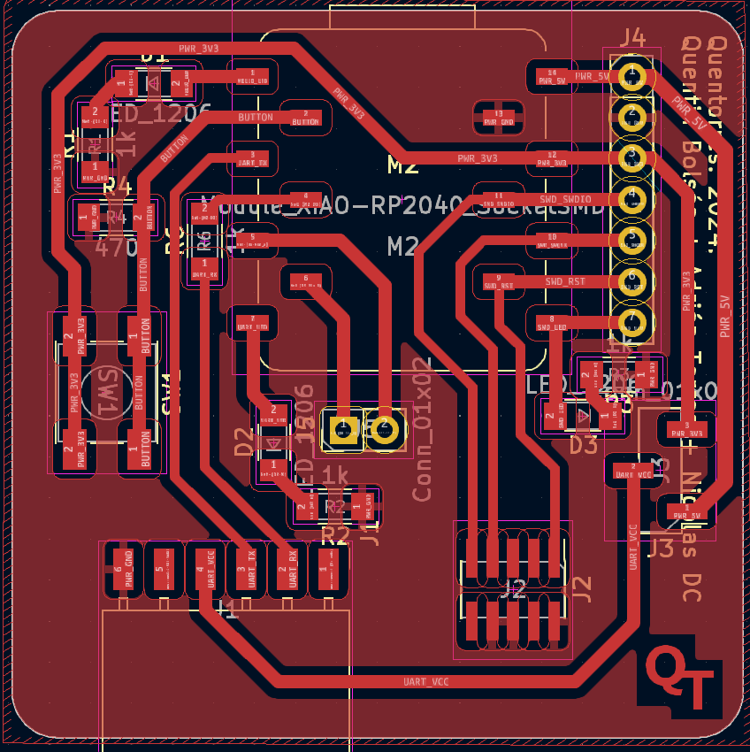
After a comprehensive review by our Fab Lab instructors (Nicolas and Axel), modifications were made to the design to implement significant improvements, particularly focused on widening the board's raceways. The redesign process was carried out in collaboration with the original creators of the project, who approved and supported the proposals. This ensured that the improvements were consistent with the initial vision and contributed to the success and efficiency of the design implementation.
|
|
| Quentorres original desing | Quentorres modified desing |
Milling the boards
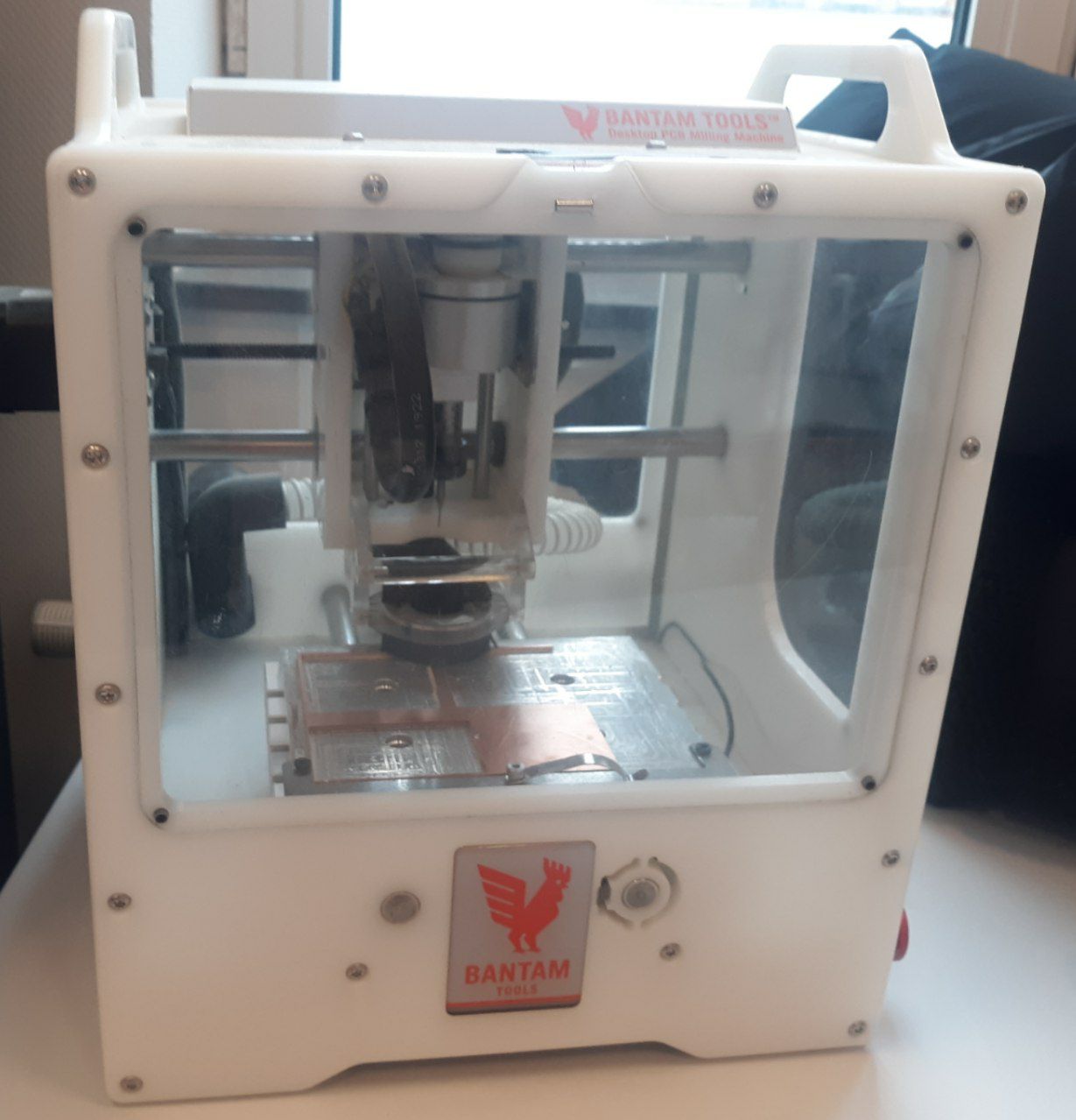
The boards were milled using a Bantam desktop PCB milling machine, series 2600.0248, as depicted in the figure:
The CNC software is used to load the file containing the design to be milled. The material to be used is then selected, taking into account its properties and milling process requirements, as well as the necessary dimensions for the part to be processed. This initial step is crucial to ensure accurate and efficient milling in accordance with the original design specifications.
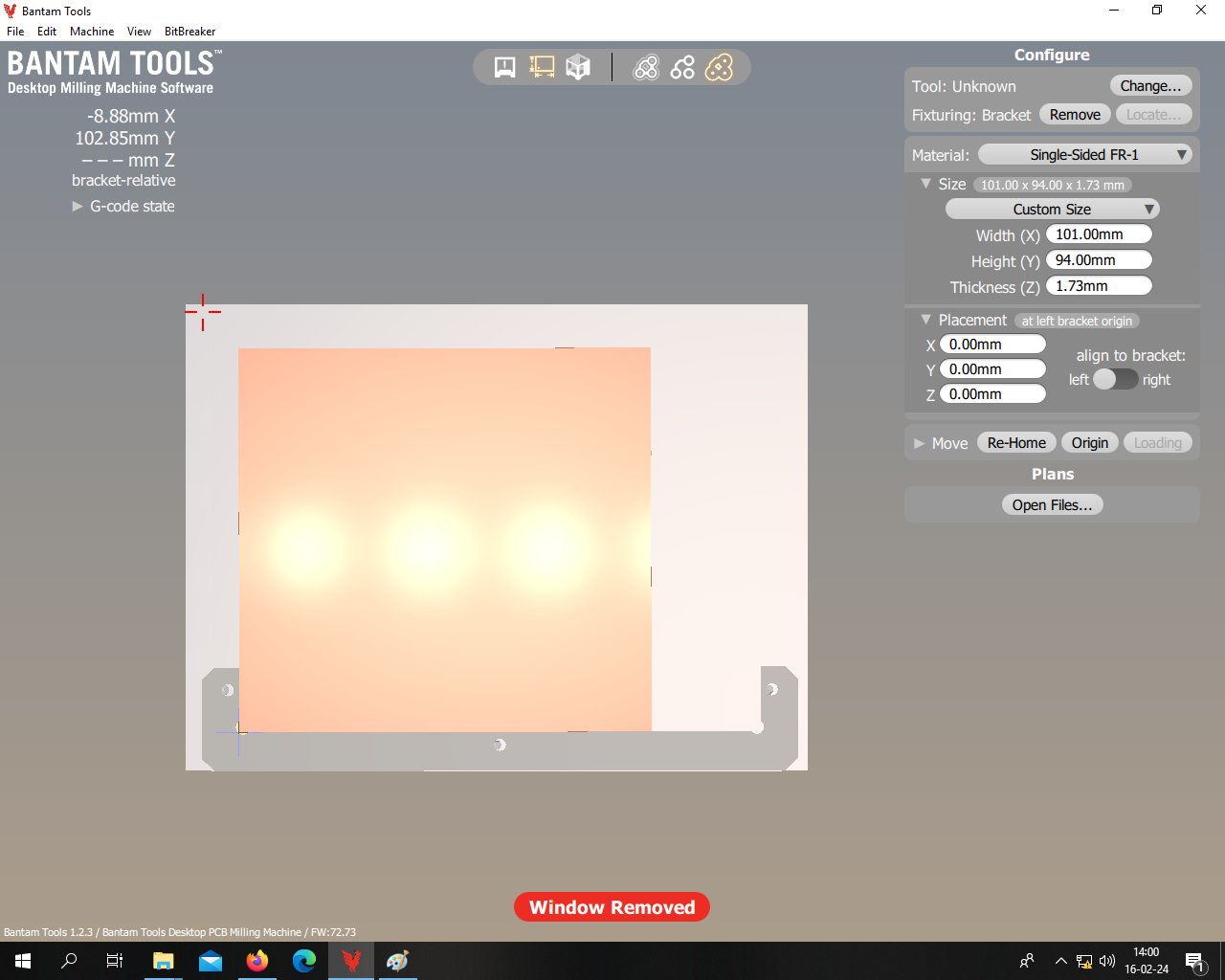
After loading the file with a .gbr extension, the design must be positioned within the work area. This step is crucial to maximize the number of plates obtained from a single piece. In our scenario, where the blank plate measures 101x94 mm, it is possible to obtain up to four designs from each, optimizing material usage and the efficiency of the manufacturing process on the CNC machine. This strategic approach maximizes production capabilities and minimizes waste.
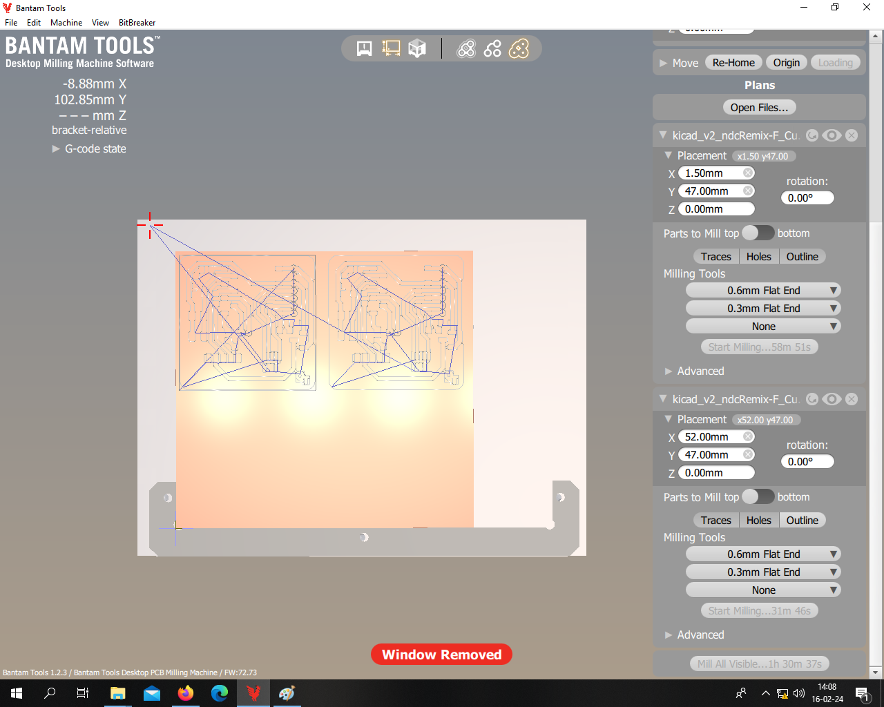
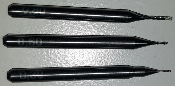
After loading the file and placing the design in the work area, the next step is to select the drills for the milling process. For drilling the 10-pin surface mount connector (SMD) holes with 1.27 mm spacing, a 0.3 mm flat end drill bit was chosen. The surface design was worked on using a 0.6 mm flat end drill bit, which included drilling additional holes. For the precise cut on the edge of the board, a 0.8 mm Chip breaker drill bit was used to ensure a clean and accurate finish on the final product. Careful selection of the appropriate drills is crucial to achieve accuracy and quality in the milling of the parts.
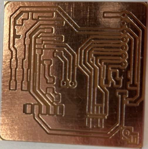
The image below displays the final result.
The initial attempt to assemble the board was unsuccessful due to the difficulty of soldering the SMD components, such as resistors and LEDs. This was caused by my lack of fine motor control, resulting in shaky hands.
During my second attempt to assemble the plate, I realized the need to protect it from natural corrosion caused by exposure to air and handling. To achieve this, I decided to utilize my recently acquired knowledge of the vinyl cutter.
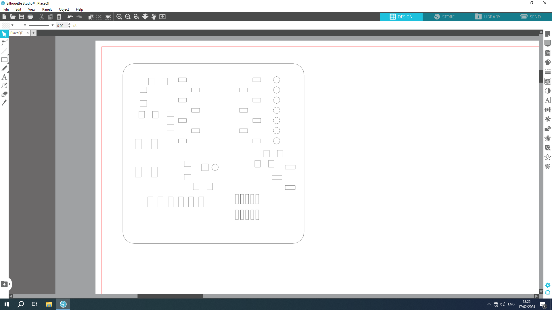
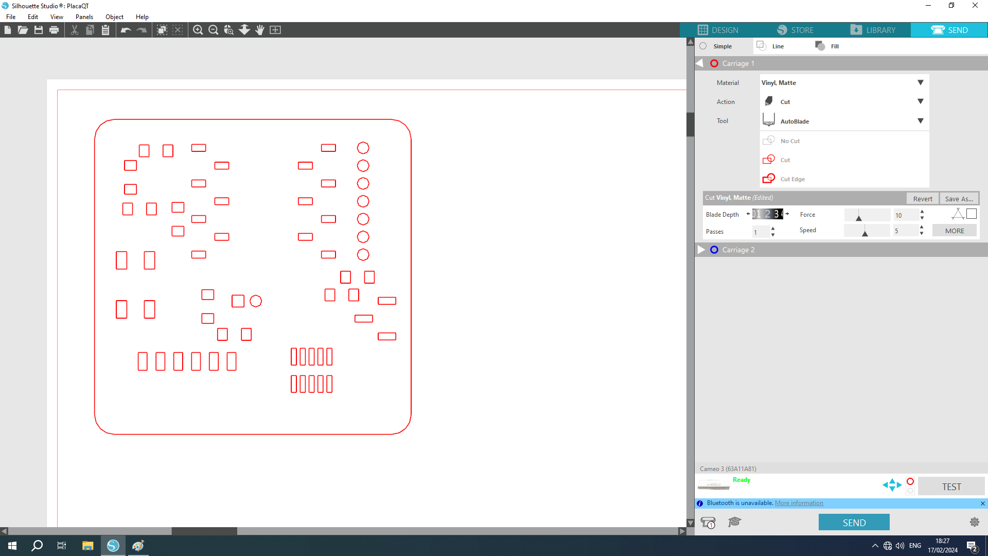
The process involved opening the .kicad_PCB file in KiCAD software and saving it in .svg format, after removing any unnecessary layers. I opened the file in Inkscape to remove the folders, group the tracings into one, and save it in .dxf format, which is compatible with the vinyl cutter used for the cuts. The attached images illustrate the process described.

File in .svg format.
|
|
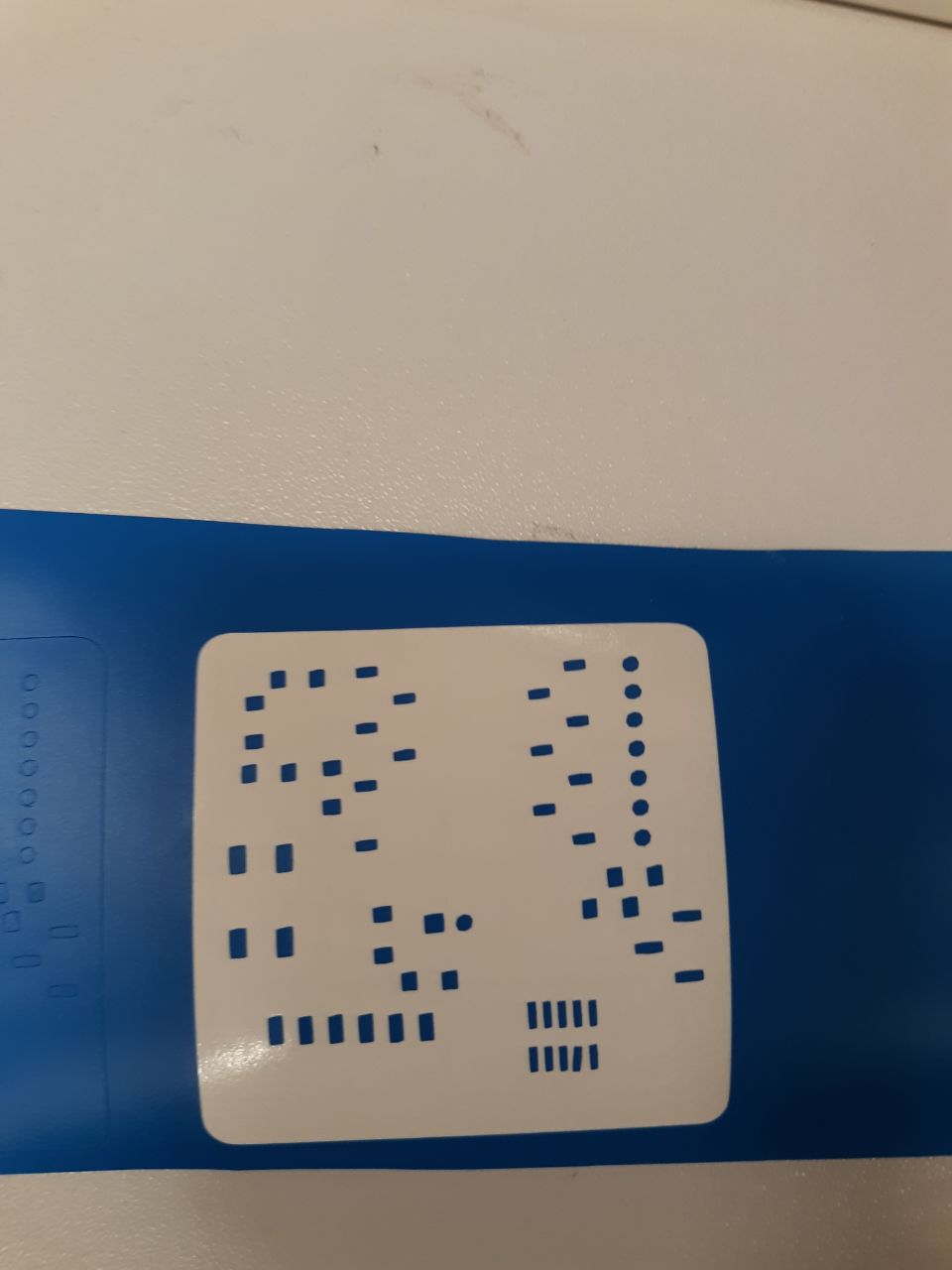
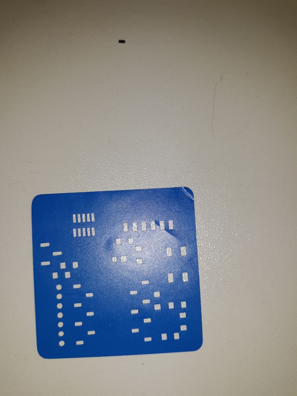
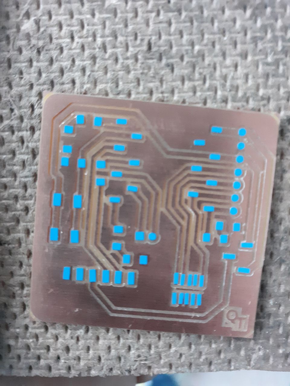
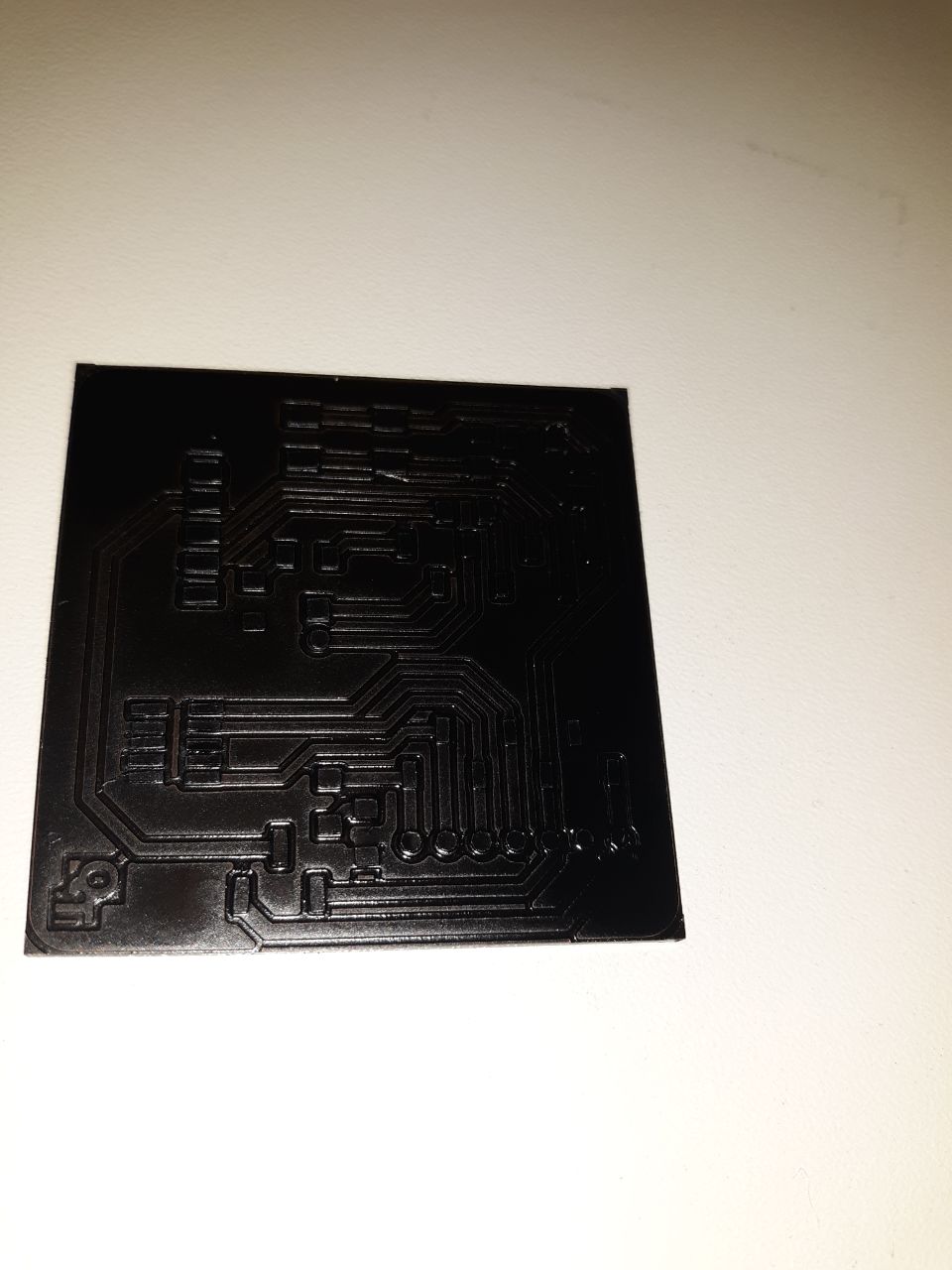
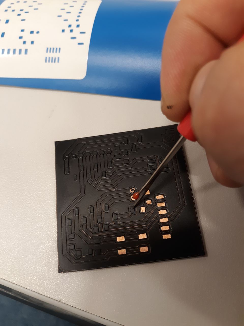
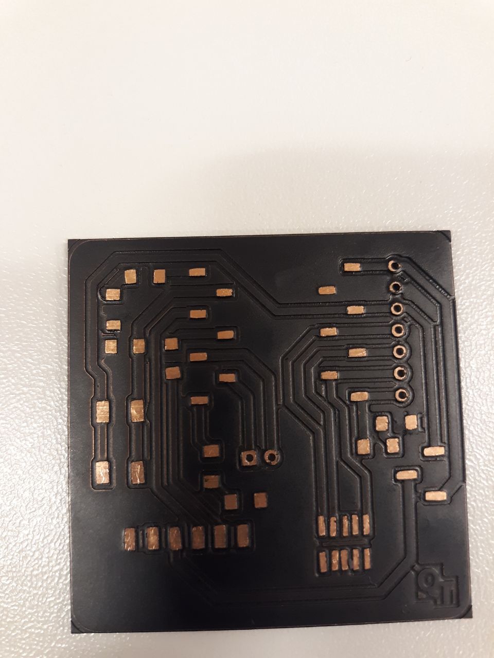
The following images illustrate the process of creating a stencil and using a negative to guide the work. The stencil is placed on the surface to be worked on, and paint is applied to protect specific areas of copper that are not to be soldered. Afterward, the vinyl is removed, revealing the final design. It is worth noting that the paint is essential in the soldering process as it helps to delimit the area where the tin will be applied. This procedure ensures precision and quality in the assembly of electronic components, resulting in an optimal final product. Each step of the process requires careful attention and precision to achieve a high-quality and durable end result.
|
|
|
|
|
|
During my experience with soldering, I encountered a new challenge. When I accidentally left the soldering iron on one surface of the board, the copper peeled off in certain areas, rendering the board unusable. To resolve this issue, I had to perform the final soldering on an uncoated board since applying the protective paint is a time-consuming process that I was unable to complete in time. Despite the setback, I plan to use the paint coating in future electronics projects, particularly in the final project, where its protective and delimiting function will be critical to ensuring the integrity and efficiency of the connections. This experience taught me the importance of precision and care in every step of the soldering process. I am confident that I will successfully apply this technique in future occasions to obtain quality and durable results. The following images illustrate the three plates. every step of the soldering process, and I am confident that I will successfully apply this technique in the future to achieve quality and durable results.
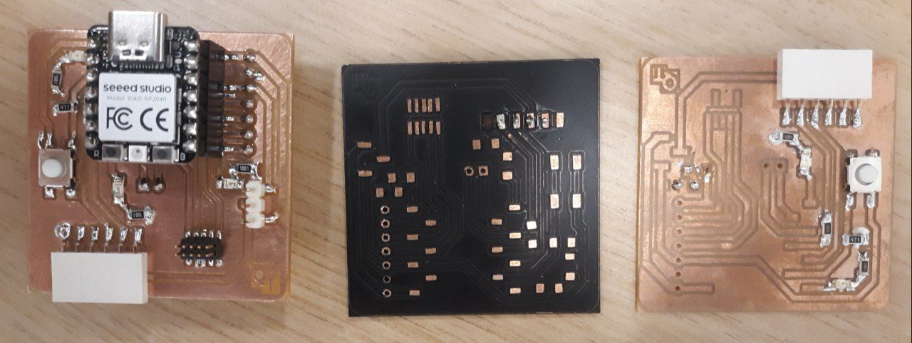
After following the steps outlined on the Quentorres project page, the final result of using the Blink example in the Arduino IDE is displayed below.
Blink Example