4. GA - Electronics production
Tasks: Electronics Production**
Group assignment:
- Characterize the design rules for your in-house PCB production process: document feeds, speeds, plunge rate, depth of cut (traces and outline) and tooling.
- Document the workflow for sending a PCB to a board house
- Document your work to the group work page and reflect on your individual page what you learned
The CNC machine
Since I am a remote student for ULB Fablab I have to do the the group assignmemt alone in SciFablab Magurele and since we are a new lab some steps (not all of them) we are doing for the first time in the lab. So I am starting with installing the CNC module on the Snapmaker 2 machine that I have used for the lasercutting, then testing and characterization.
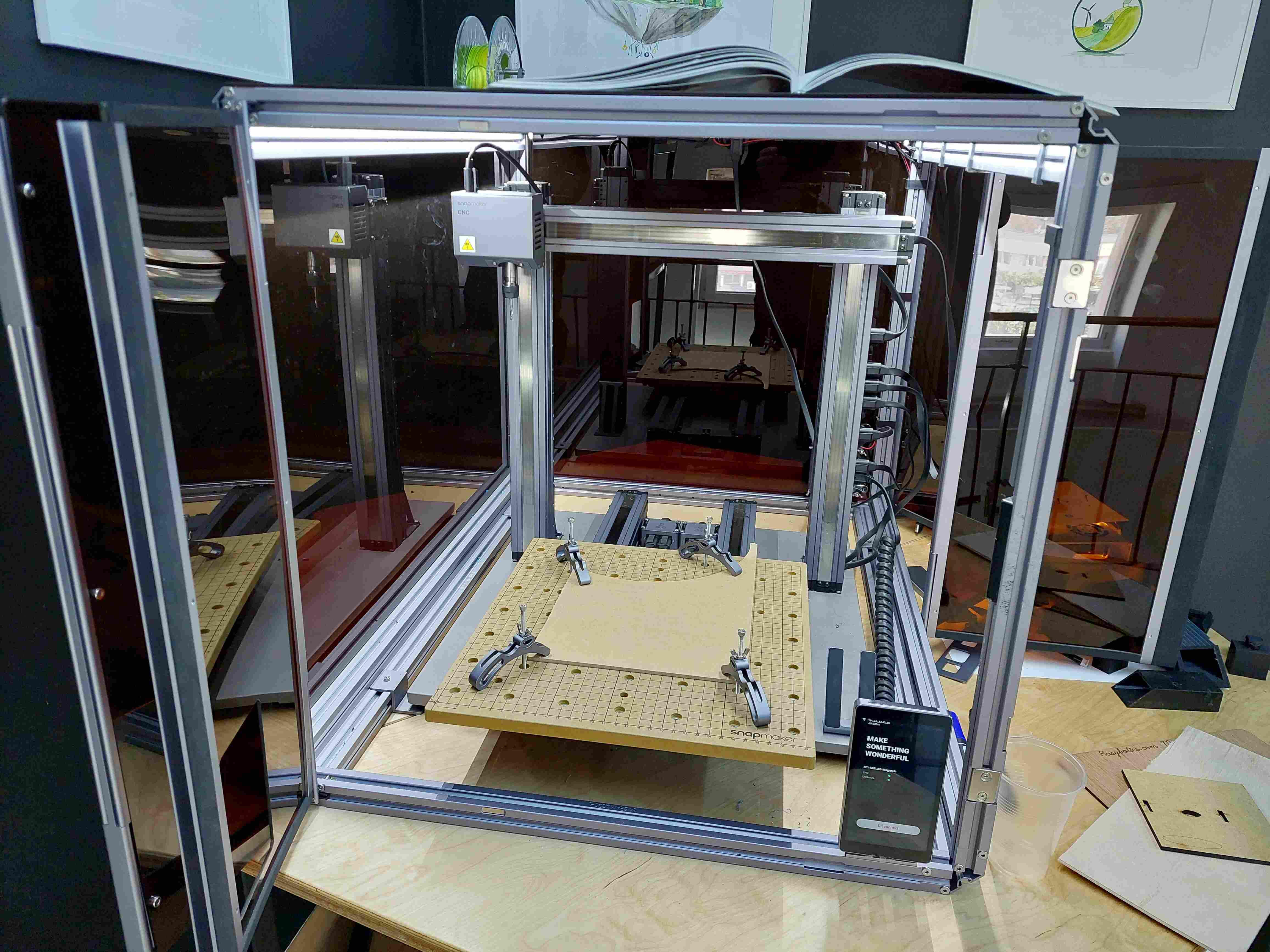
- Model: Snapmaker 2.0 A350
- Software: Luban 4.10.2 😎
- Specifications: Max. operation area: 320 mm (X) x 350 mm (Y) x 330 mm (Z), Mechanical Resolution 0.03 mm/step, Revolution speed 12,000 rpm, layer resolution is 50 microns–300 microns.
- Tools: V-bit Milling bit 0,3 mm; Flat end mill Milling bit single flute, 1,5 mm
- Materials: MDF boards and, FR-4 Printed Circuit Board 15 x 10 cm.
Installation and callibration
I am removing then laser module with the CNC module, it is using the same fixing system, and also the bed has to be changed.

prindere bed

Setting the origin X, Y, Z

Luban workflow
Characterization tests
Type of bits

Dictionary
Table dictionary
| Term | Definition |
|---|---|
| jog | |
| shaft |
Testing on wood
Menius with settings and steps

Testing on epoxy board
copper 0.5 oz: 17.5 um 1.0 oz: 35 um 2.0 oz: 70 um
First trial
I am running the test file on the epoxy board with the following parameters. Now, I intend also to cut the board so I have to take into considerations the exterior lines. I am not sure at this point what is the right procedure, if to cut with the same bit or to change it, I am in trial mode. The width of the board is 1 mm, I am trying with a “step down” of 0.5 mm, which means two passes.

Parameters for the traces
tool diameter: 0.3 mm cut depth: 0.07 mm
And for the path to G-code cell: cut speed: 300 mm/min plunge speed: 300 mm/min step down: - stepover: 1.2
For the jog jog speed: 1500 mm/min jog height: 1 mm stop height: 8 mm
Parameters for the exterior line
tool diameter: 0.0156 in cut depth: 1 mm
And for the path to G-code cell: cut speed: 300 mm/min plunge speed: 300 mm/min step down: 0.5 stepover: 1.2
jog speed: 1500 mm/min jog height: 1 mm stop height: 8 mm
With these parameters the test fails in several ways, in the most parts it didn’t remove the copper layer, then it did’t cut through the board. I try again changing the following parameters.
traces: cut depth: 0.14 mm exterior lines: cut depth: 1.2 mm
The result, it didn’t cut through, it removed the copper layer but still not uniformly. It is ime for a debugging pause:

Debugging
So far I thought that working with some defaults and skipping the details would take me to an easy result. The fact is that I skipped over a lot of questions that I had means that I have to check if they influence my result.
- At this point I admit I don’t know what the numbers engraved on the board meaan, are they absolute values, or relative, is it the length of the design fixed or it can be varied according to the bit size we used?
- Then copper removal is not uniform, it is cleaner toward de center, that might mean that I have a bending of the board in the up direction in the middle.
- Then I am suspecting my toolpaths, they are all parallel with the X axis as if the machine can’t do smooths rounded paths and only it does straight lines and right angles. I am also suspecting the resolution of the files.
Raising all these questions it takes me to more experimentations, looking for tutorials and trying more tools. I am doing some changes.
I changed the fixing method of the board going to the double sided tape
Check for different displacement direction of the board and positionings;
- use vector files as input for Luban, it is a marginal improvemnt onlu, then I try using mods and reading/visualising the gcode with nviewer
- try milling the board v1, to see how the performances impact on the test impact my board. It is horrific.
Mods does the difference and gives me more rounded passes, I am giving up Luban the part of gcode generation; I use only the workspace/job controlling interface.
The mods is better on v1 board but still unusable, I am switching to v3, ULB version, which is a version with thicker paths, but here I only have the gerber file which Luban doesn’t know how to play it. I convert it to png and feed it to mods, the result is bad again but I believe the fill prameter is wrong this time.
I go to Flatcam and watched a tutorial.
The development board
Task and materials
| Components | Image | Amount |
|---|---|---|
| SEEED STUDIO XIAO RP2040 |  |
1 |
| CONN HEADER SMD 10POS 1.27MM | |
1 |
| CONN HEADER SMD R/A 6POS 2.54MM | |
1 |
| Tactile Switch SPST-NO Top Actuated Surface Mount | |
1 |
| LED BLUE CLEAR 1206 SMD | |
3 |
| RES 1K OHM 1% 1/4W 1206 | |
4 |
| RES 499 OHM 1% 1/4W 1206 | |
1 |
| CONN HDR 7POS 0.1 TIN SMD* | |
2 |
PCB milling
Soldering the components
Testing the board
Conclusions
Checklist
- Linked to the group assignment page
- Documented how you made the toolpath
- Documented how you made (milled, stuffed, soldered) the board
- Documented that your board is functional
- Explained any problems and how you fixed them
- Uploaded your source code
- Included a ‘hero shot’ of your board