Electtronic Designed
Make Something interesting
Group assignment
The group's tasks:use the test equipment in your lab to observe the operation of a microcontroller circuit board and send a PCB out to a board house fablab website.
General Objective

The idea is to make a simple system based on the esp32+lora with some inputs/outputs for motors, LEDs, sensors, etc... that can be used to continue using it in the coming weeks and that is scalable.
Before Design
It is good practice before designing or building a circuit, to simulate it to check that it works as desired. There are many simulators today, each with their respective strengths, but for today's example we will use wokwi, a simulator in the cloud, free and very easy to use.

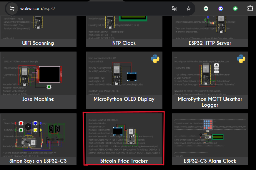
Once the Microcontroller to simulate has been selected, we can select a blank environment or one of its example templates, so I selected one that looked similar to the main idea and made some modifications to it.
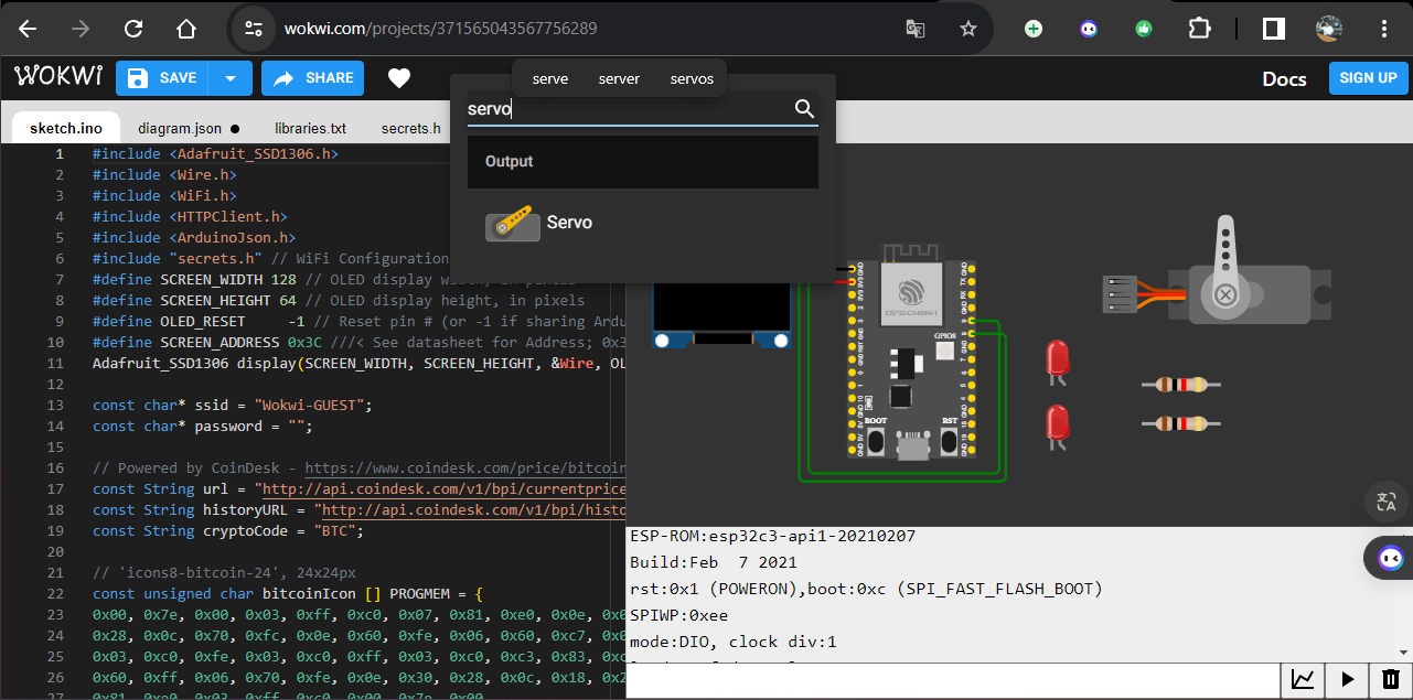
UOnce inside with the plus button we can add the necessary components, write the code in the windows while we see in a quick and controlled way what would happen.
With the components selected, we delete the code that does not interest us and start testing to see how it goes.

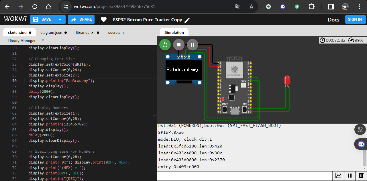
Once all the components have been installed and their connection and operation checked, then it is time to design the circuit.

There are many PCB design software, among the most notable we find Altium, one of the most popular among professionals, kicad, without a doubt the main one in the maker community and independent developments and Proteus, one of the most used in the teaching field due to its ease of combining design and simulation in a single program, just to mention 3. In the end it will be the last one in which I designed my PCB.
Like most PCB software, you start by designing the schematic, a classic cad sheet with the usual tools, such as lines, texts and figures.

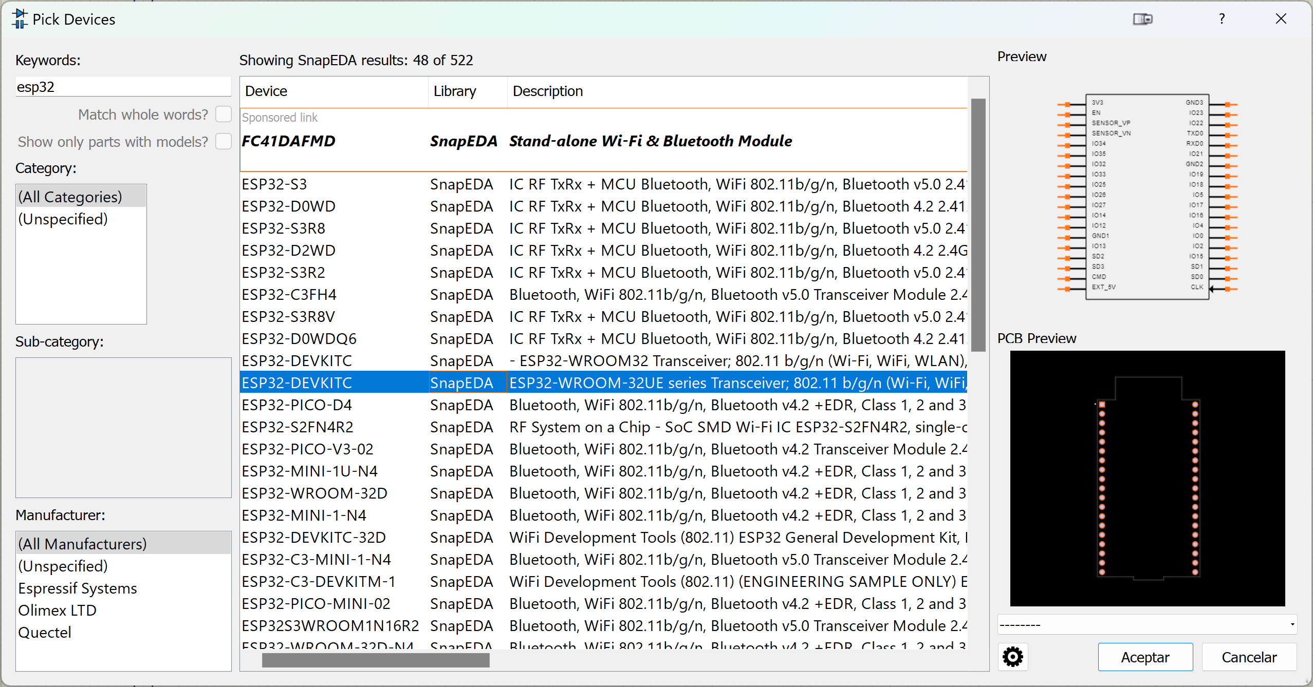
With the component tool, new elements from both local libraries and the Internet are added to the diagrams. In the specific case of my board, I don't have it locally and I will probably find it on the Internet, but I decided to do it myself.
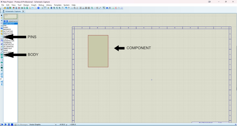
FIt is a very graphic process, where I draw a rectangle to give it shape, then I place the pins and name them, finally I name the new component and it is ready to be used.
Since the rest of the components are generic, we look for them and put them in during the work hour. Finally, we add the ground, power and labels and we are ready to move on to designing the PCB.

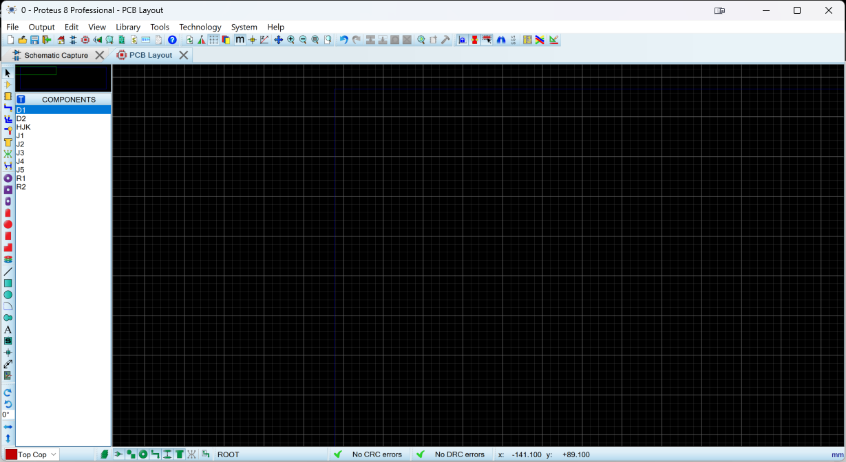
This new sheet is another classic CAD, with line, figure and text tools. Generic components have a footprint assigned by default (although it is editable, of course), and the components that you design or add must be created. In this case you have to create the microcontroller footprint.

To do this we will take the rule to establish a specific separation, we will put the pins that the component needs (it has to match the schematic), once we have it ready we can add as much aesthetic detail as we want but in my case I will only put a border to guarantee that it does not collide with other components.
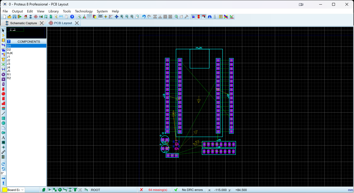
With the prints ready, we place them in the work area according to the layout and shape that we want the PCB to have, trying to ensure that those that are related remain together.
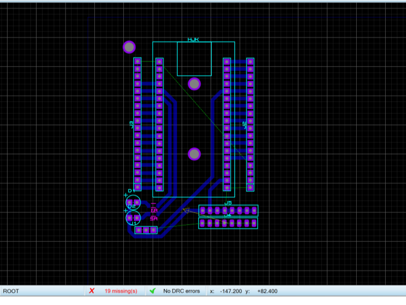
The most important part of this selection is the layout of the tracks, where one component is linked to another, the track thicknesses are established, where a greater thickness is generally defined for the power tracks.
To avoid adding a street, to make the CNC work less and to reduce electrical noise, we will put a ground plane on the PCB, a solid section that occupies everything that is not a street and that transmits the GND of the circuit.
In the final touches we will put a border on the PCB, some bolts to hold it and we will move on to the 3D visualization.
TIt looks good but clearly the components I created are missing and some are not as they should be, so I will have to edit those components.
The first thing will be to go to this grabcad website and search for our component model, once located we download it in step or gxxx format.
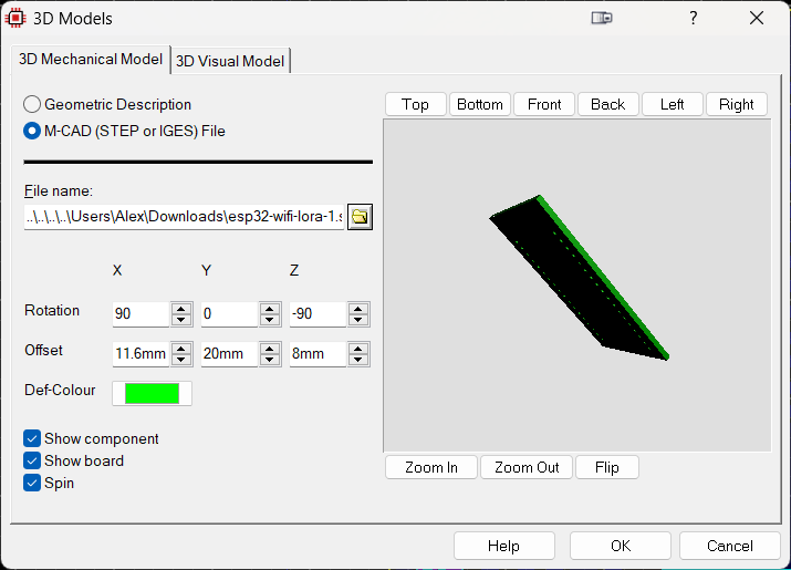
When editing the component properties we see that you can select its 3D model, once located in the download folder we adjust it to the PCB.
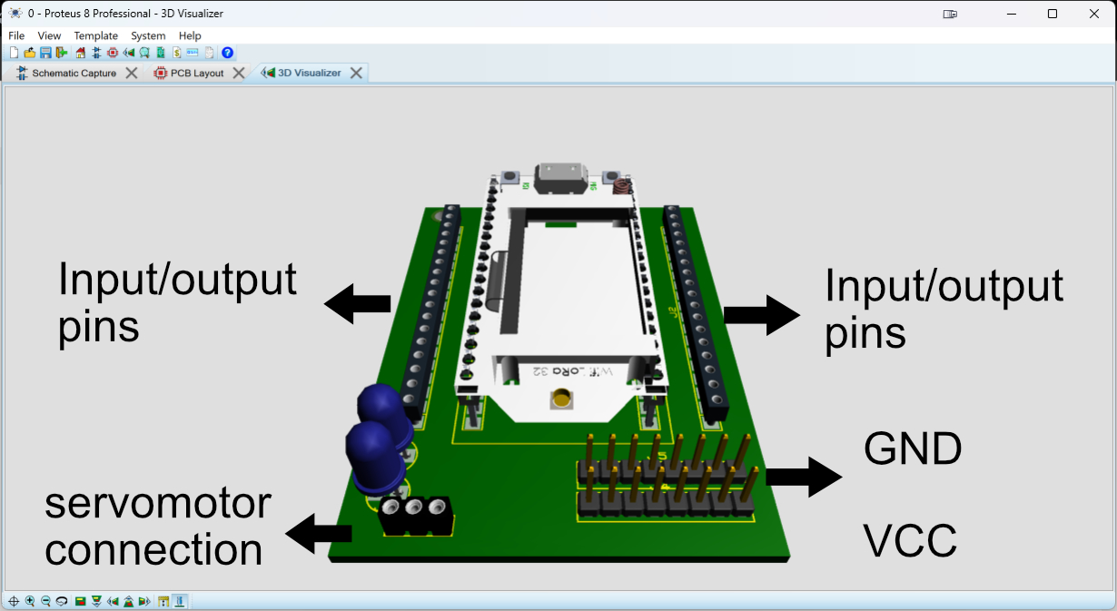
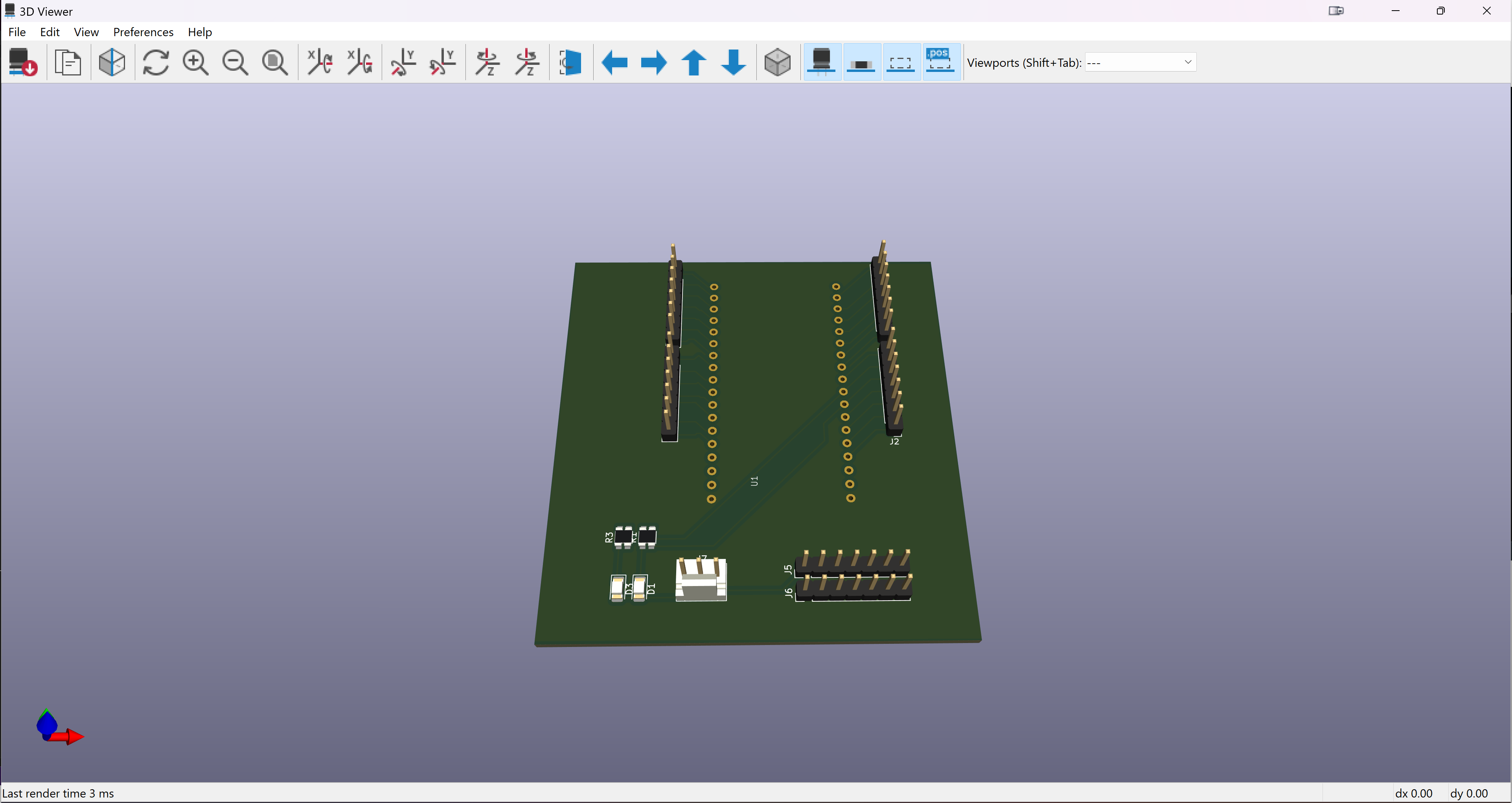
Now if the PCB is quite similar to what it should be, let's see if it looks like this after manufacturing it.
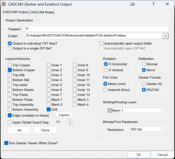
To manufacture it we click on export gerber, we select the layers we need and follow the steps of the Week 4, where I explain how to manufacture a PCB on the CNC or by acid solutions.
It is not a very complicated piece, the manufacturing took just under two hours, but it turned out very well.
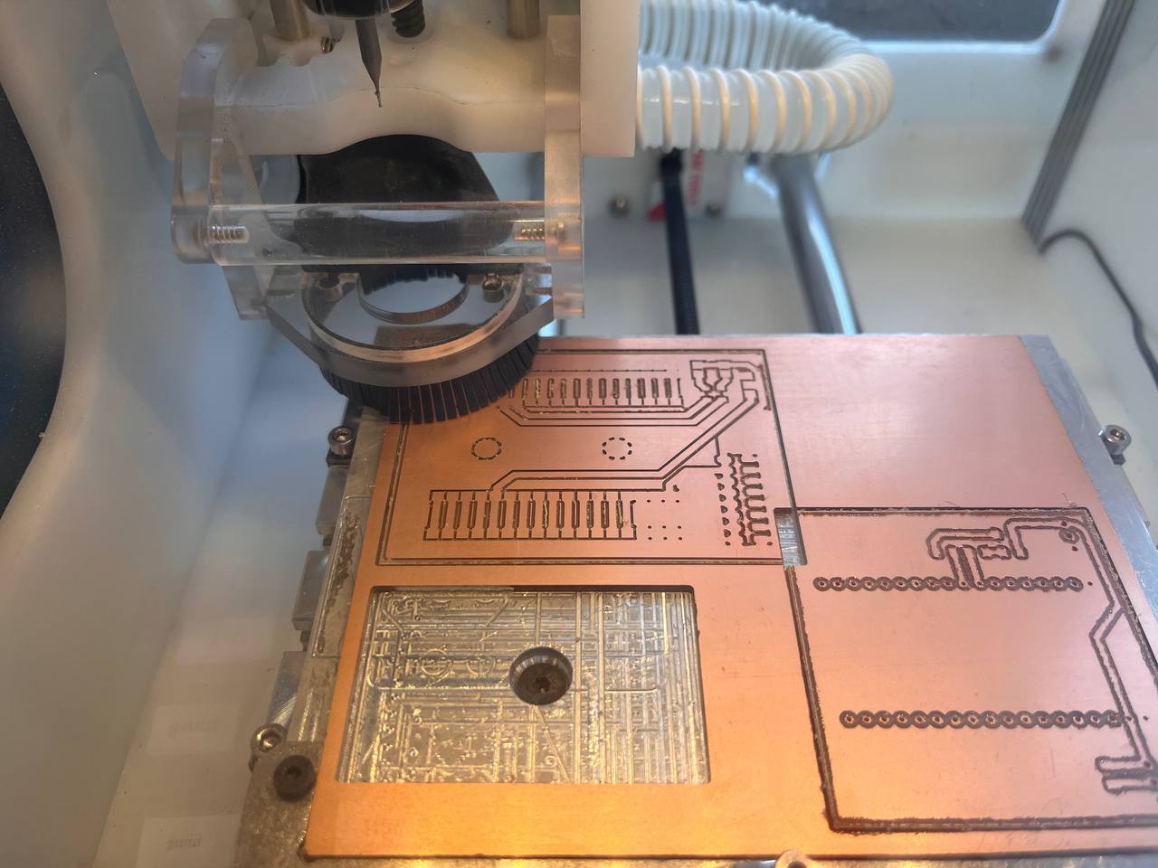
Unfortunately there was a problem with the drills so I had to end up making them by hand.

The components fit together perfectly, we will see how the soldering turned out later when we supply it...first, we are going to try other electronic design software.
Although the meme was funny, the reality is that Kicad is widely used by the community and since it is free it has a lot of online documentation, so I will make another version of the project in Kicad.


Everything is quite similar to Proteus so I will start in the schematic where we will create the microcontroller, because it is not native either.
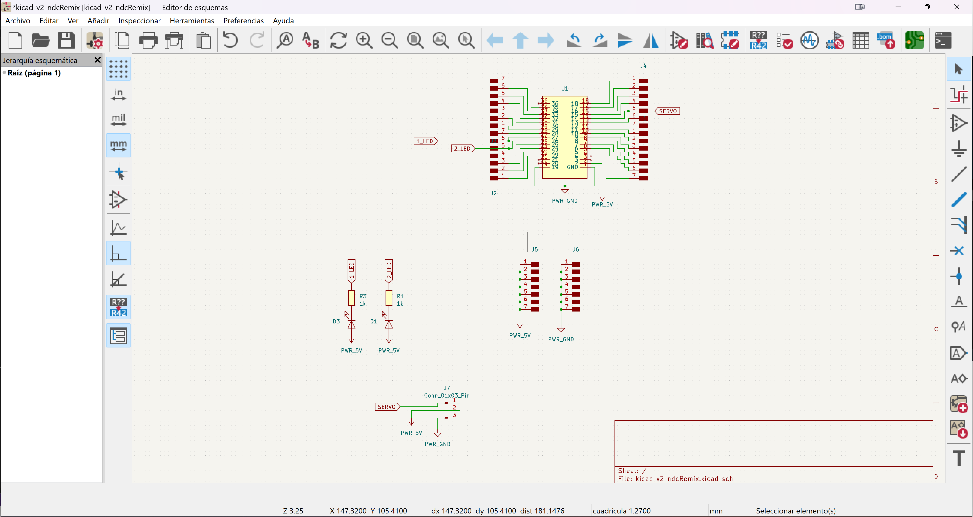
Once the component is created, we move on to put the rest of the elements of the PCB, I will make it the same as the previous one so there will be some connectors with 2 LEDs and their resistors.
An important important difference here is that the footprints must be assigned, or they can be indicated automatically but it is not ideal.

When we finish the schematic and update the PCB, this view appears with all the components so that we can group them and place them as we see fit.

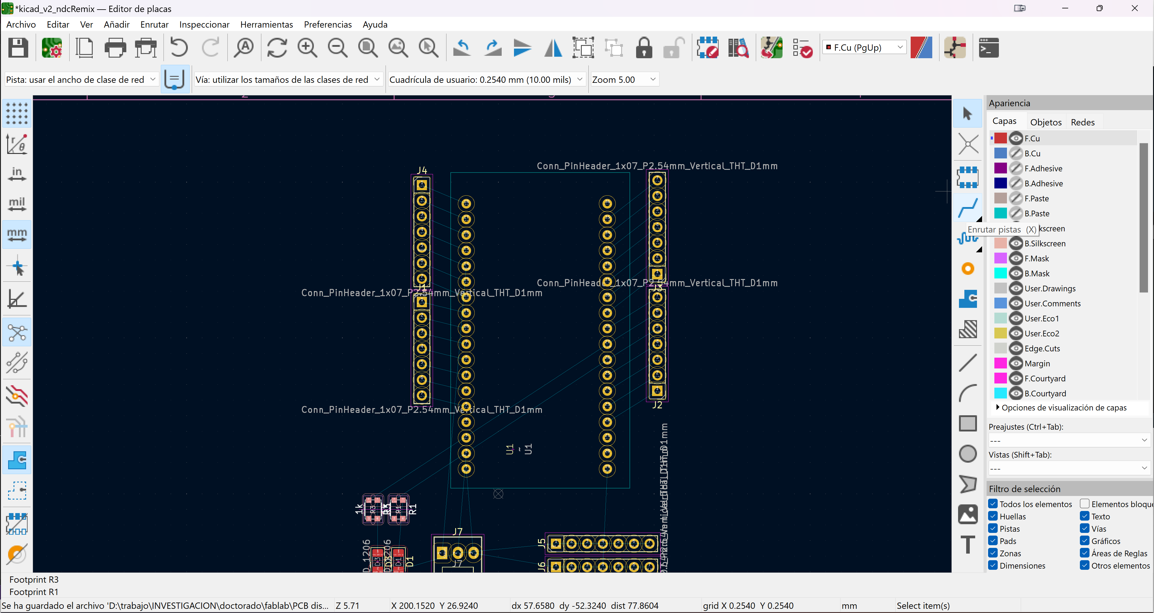
Once the components are placed, draw the streets, it is all very similar and it is an almost the same process.
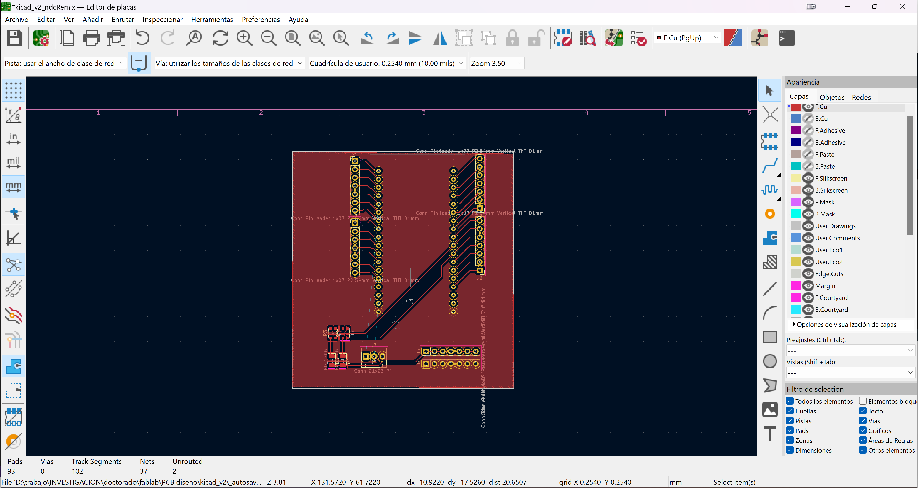
To finish, I place the ground plane and make the final adjustments, I won't do much more because I won't make this version.
Finally this is the result, it is good, comfortable and I think that even more than in Proteus, I will not look for the 3D components because that is fine for one test, I will use the other to continue.
Naturally, the need arises to make a protective case, for this we will take the design that we just created and export it in STL (it is not ideal but it is the best, it worked for me in fusion), once opened I will design the box with the tools described in such week 2
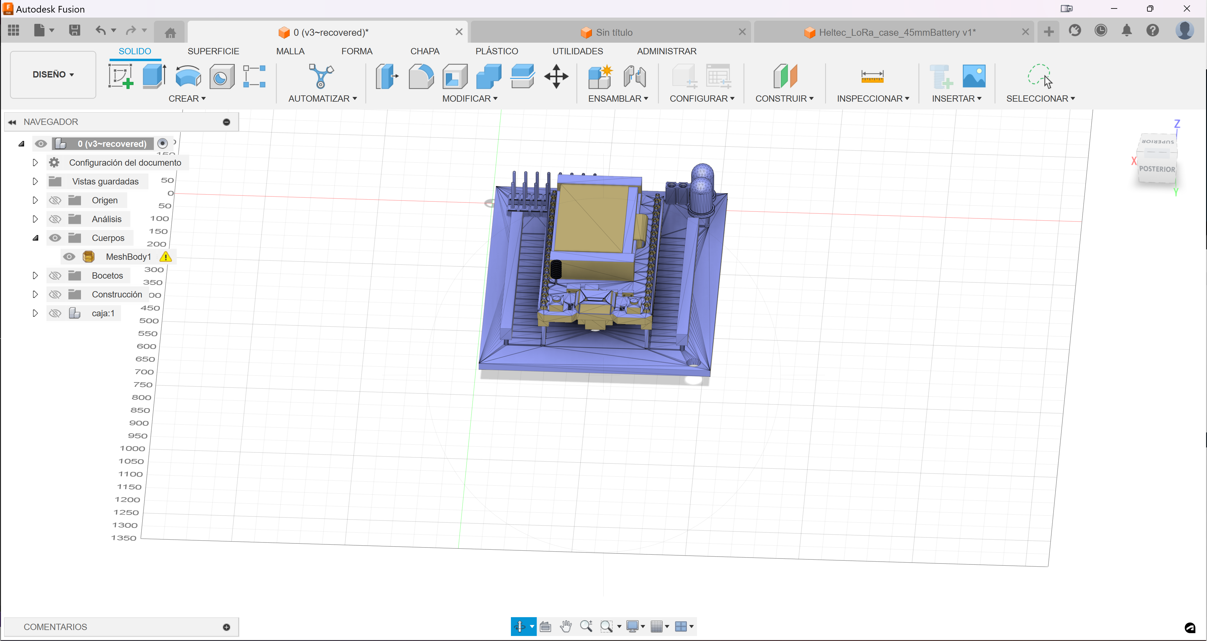

Once the outer contour is made, we will use the gap tool to create clearance between the PCB and the casing, and with this ready we can move on to making the extrusions and cuts.
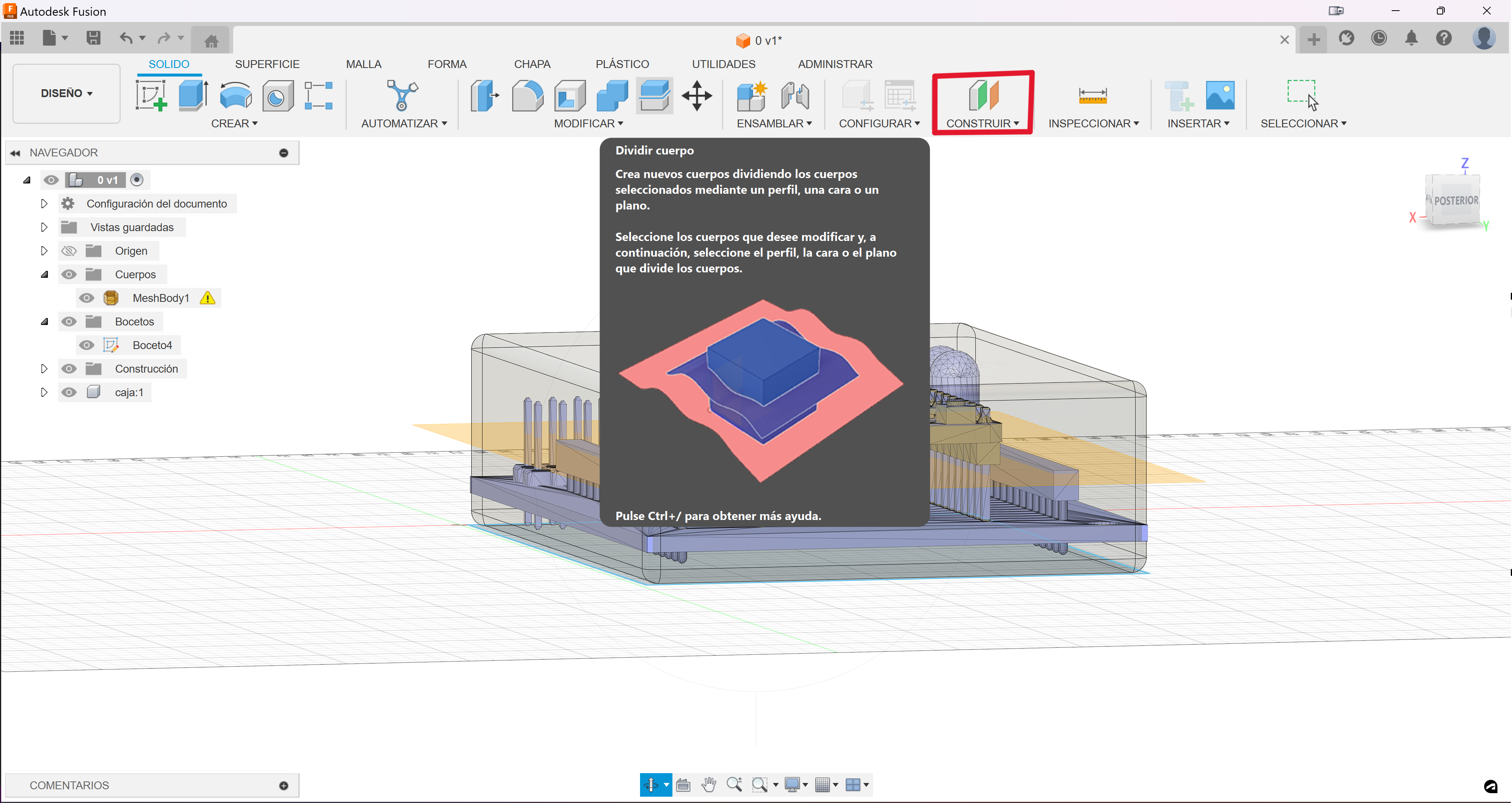
To convert the block into two parts of a box we will draw a plane in the middle plane and cut the piece in half.
After all the cores are finished, we embellish them with the splicing tool.
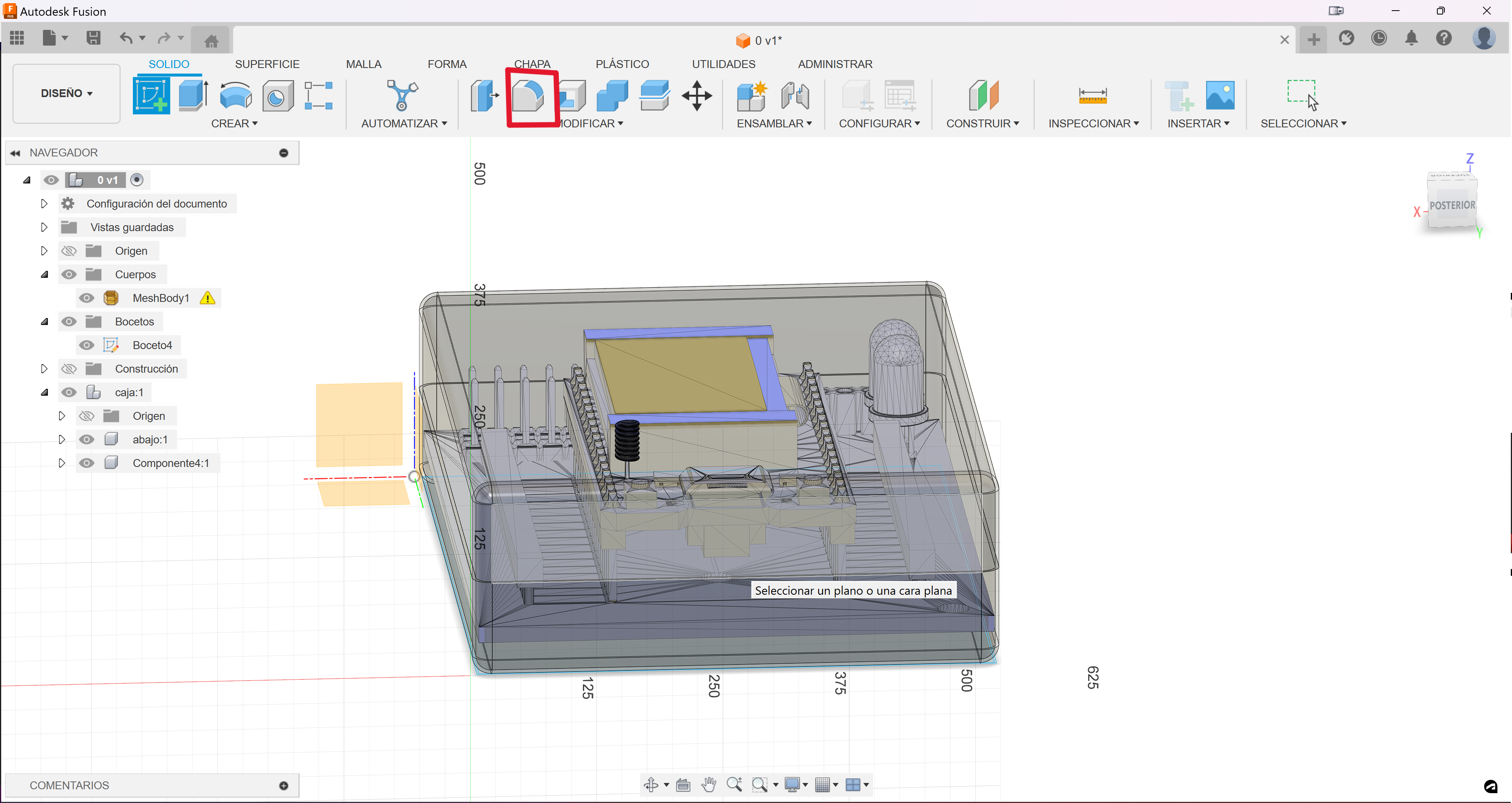
To close the box we will draw some small checkpoints with the line tool, for which we will do a selection analysis to work more comfortably.

gft.png)
Once the box is ready we can make a render of it just by going to that section, I imagine that the parameters of it can be changed but even without doing so you will be satisfied with the result.
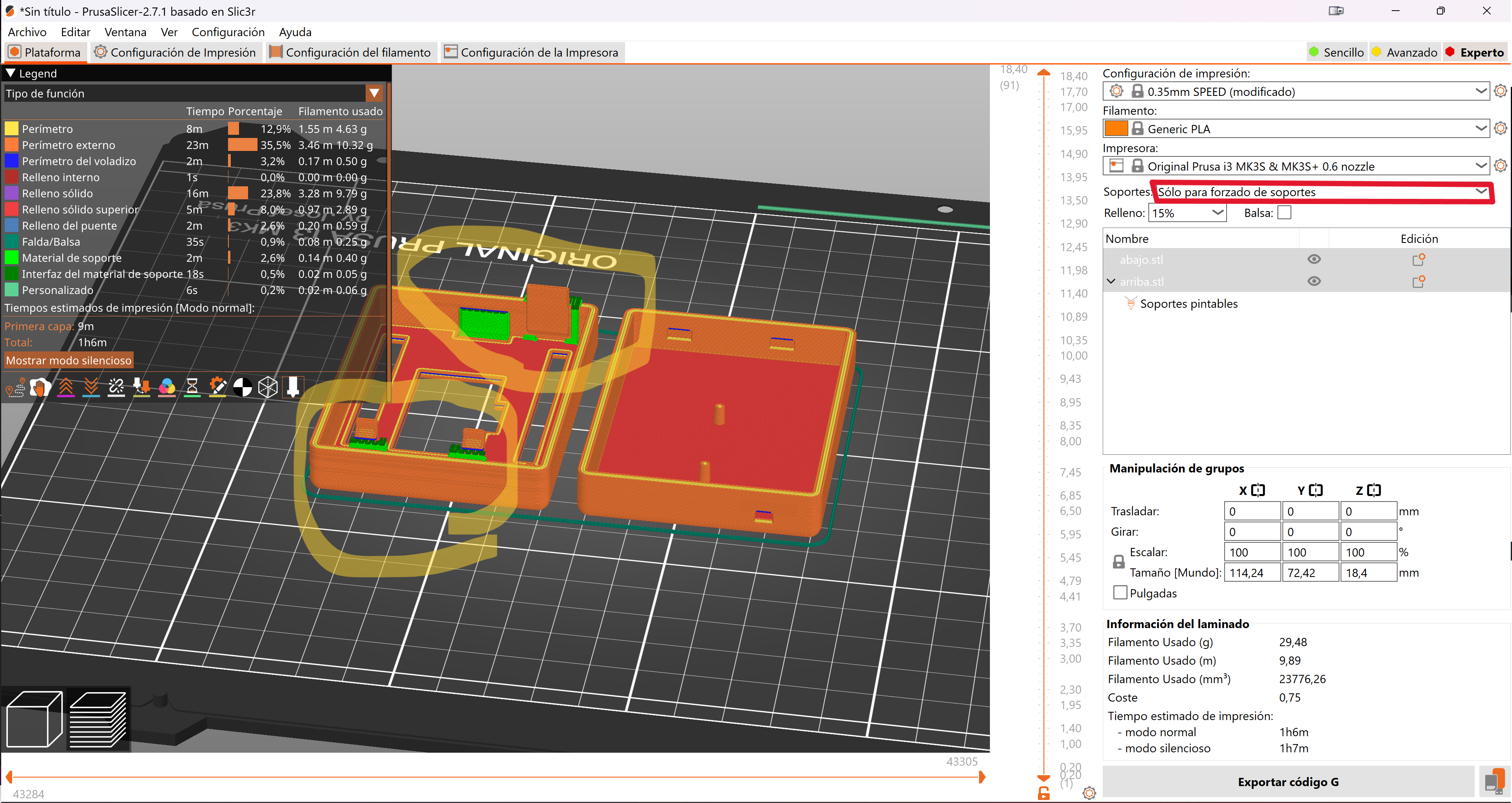
Consistent with the design, I moved on to the manufacturing of the piece. For this, I laminated the piece with the PrusaSlicer laminate, maintaining the default configurations and only adding some supports in the indicated places.
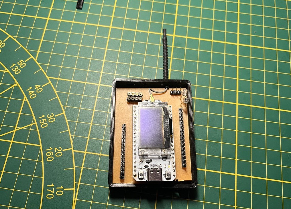
Once manufactured, it was quite the same as the render, I had to use a little force but it is acceptable.
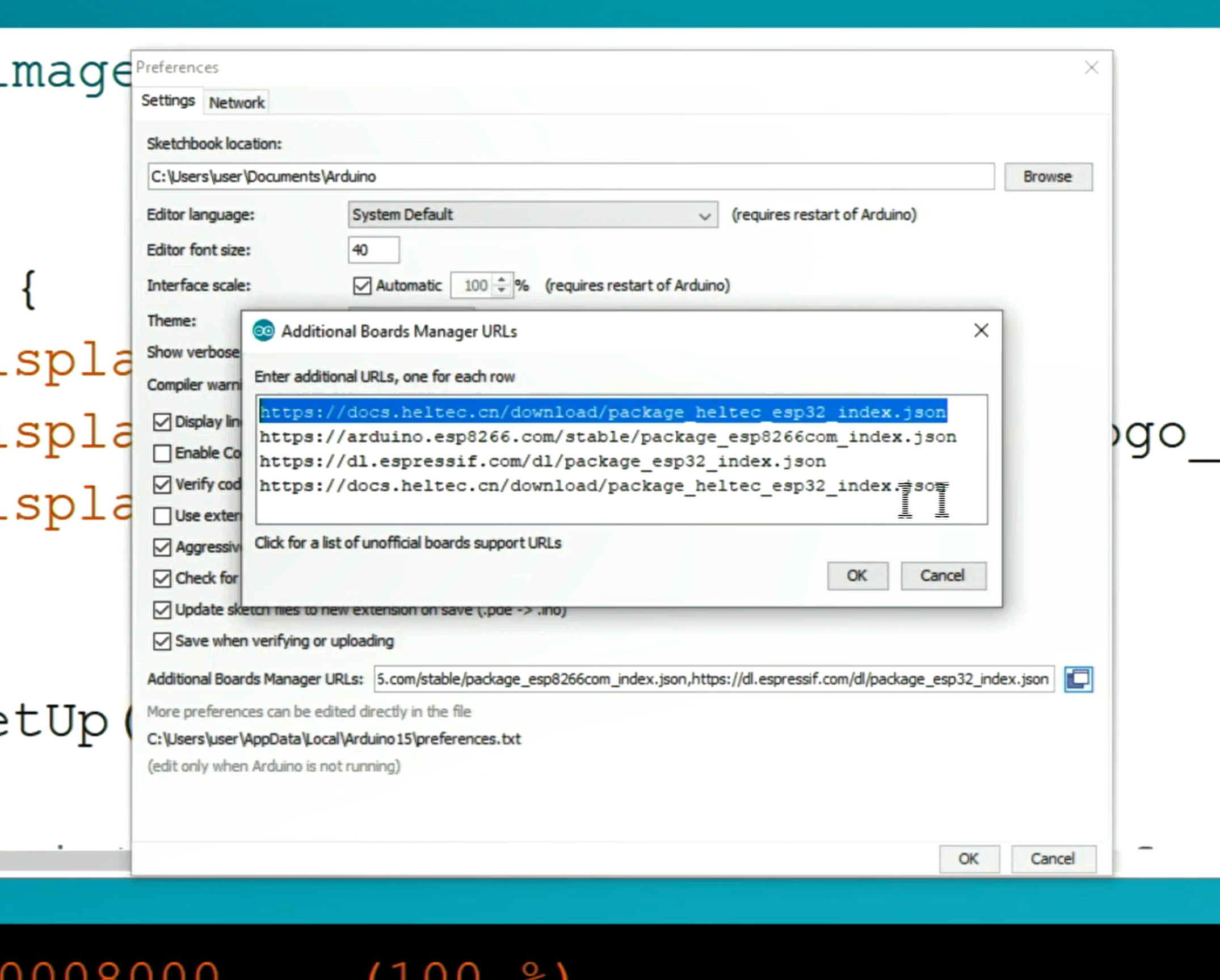
To test the board we uploaded an example code of the board, which to add it you have to go to preferences and add the following line: https://docs.heltec.cn/download/package_heltec_esp32_index.json .

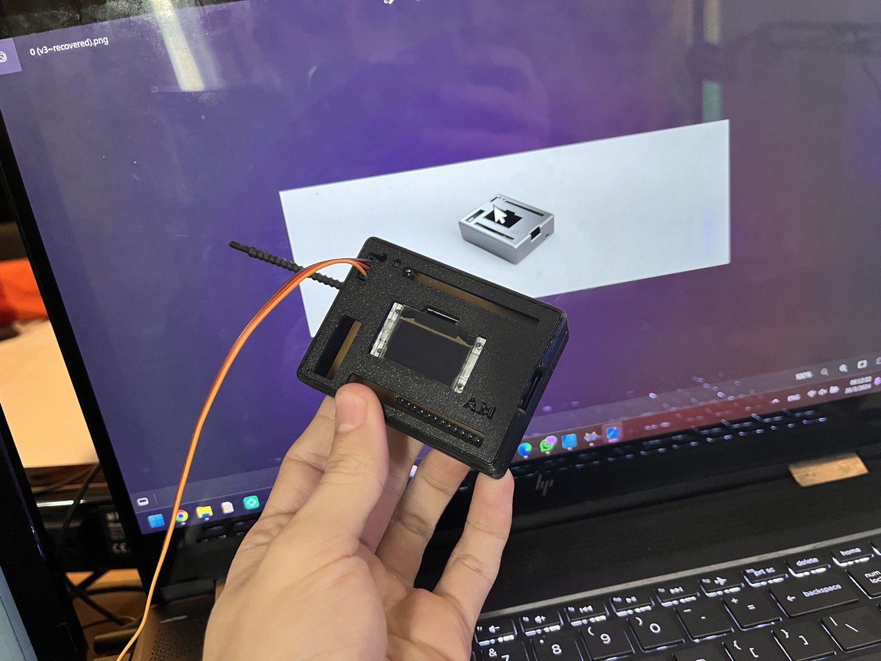
Since the objective is to use this board in several projects, I will need another one to test the communications, so I designed another box for a new module.
The objective of this new one is only to communicate with the original one, which is why at the moment it does not have a PCB, just a battery and a switch.

We finally see the result of the week and the promise of seeing both boxes interact in the future.In this link I leave all the files generated this week