Electronics Production
It is possible and it is here
Group assignment
The group's tasks: characterization of the design rules for the internal PCB production process and sending a PCB to a board house can be found on our fablab website.
Starting production
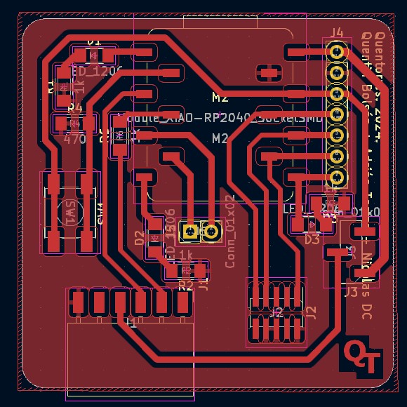
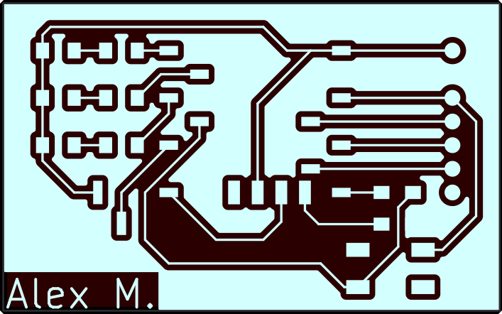
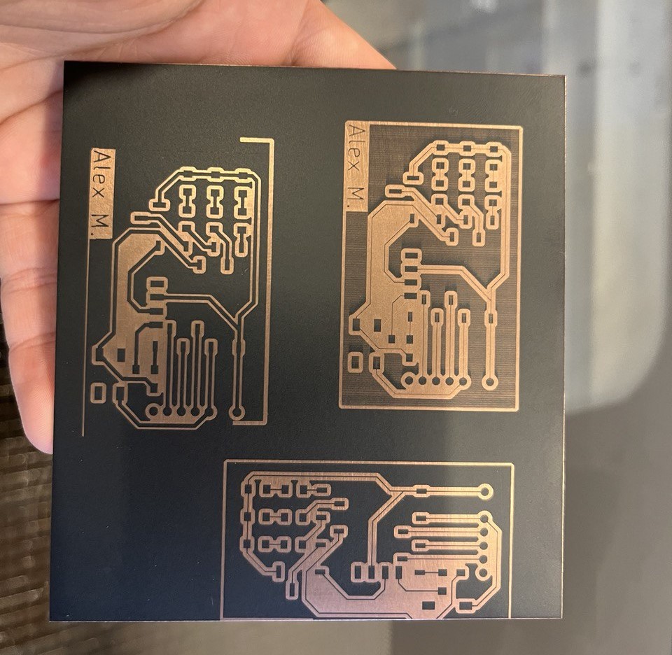
The objective this week is to manufacture a PCB, for them we will start from The Quentorres project that represents a technical challenge and a significant learning opportunity. The specific version of the PCB that was chosen to replicate included modifications made by my instructor Nicolas. To carry out the PCB replication, I had several Gerbers at my disposal. However I chose to work directly from the KiCad file. This choice was motivated by my desire to delve deeper into KiCad PCB design software, a powerful and widely used tool in the electronics field.
Starting production
The designs made on the original project can be considered minimal, I set the width of the tracks at 1mm, eliminated some components, changed the trajectories of the routes and put my name.
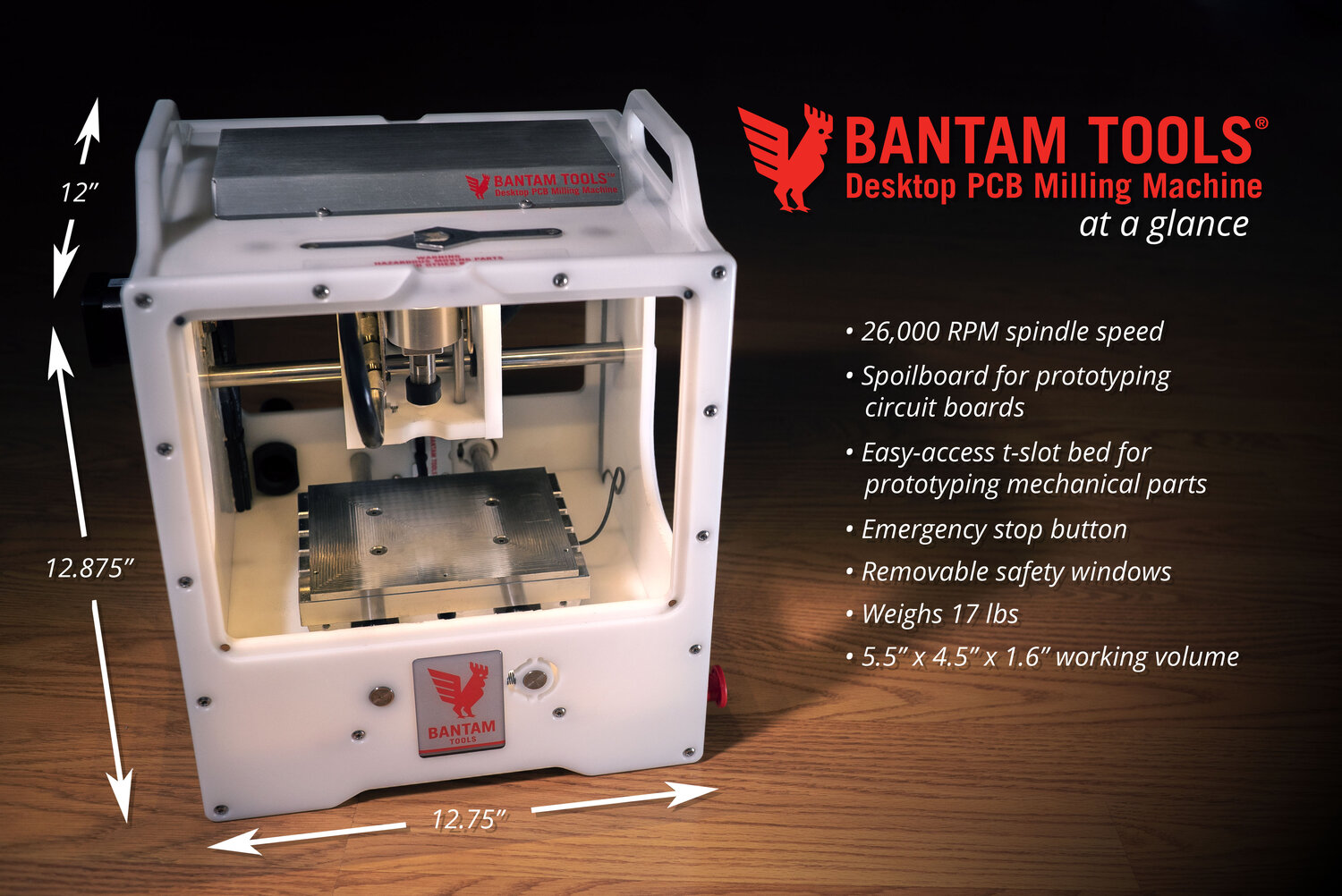
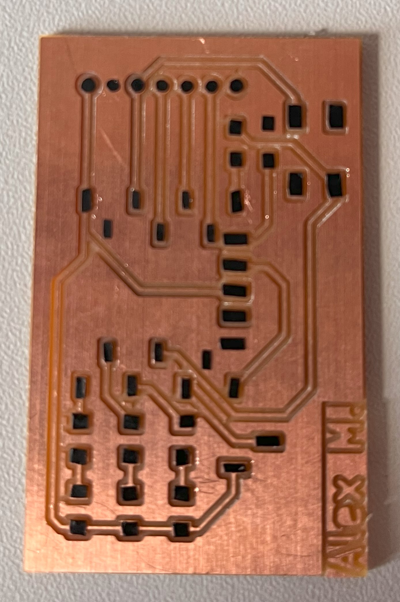
Producing PCB prototypes using CNC milling machines is a common practice due to its efficiency and precision. In particular, the Bantam milling machine, located in the ULB FabLab, is designed specifically for this purpose, significantly simplifying the PCB manufacturing process.
This PCB manufacturing method is ideal for projects that require rapid iteration and proof of concept, allowing designers to experiment and optimize their designs effectively. Additionally, the ability to produce high-quality boards in the FabLab itself encourages a self-directed, hands-on learning cycle.
Steps to manufacture PCB
To coordinate and detail the general steps to manufacture a PCB with the CNC milling machine, we could structure the information as follows:
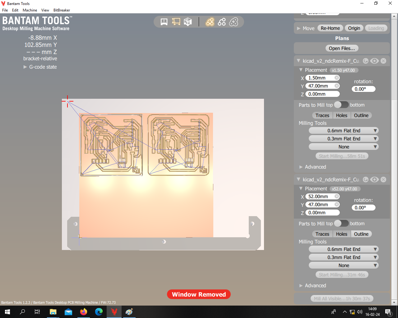
1. Gerber File Import (GBR): Start the CNC milling machine control software and Import the GBR files corresponding to the PCB design.
2. Selection of Tasks and Tools: Determine the necessary operations, such as copper stripping, drilling and contour cutting, and we must choose the appropriate tools for each task, such as drill bits of different sizes and types.
3. Manufacturing Parameter Adjustment: Setting the speed of the router to optimize precision and avoid damage to the material and adjusting the depth of the scribe to ensure that the tracks are engraved correctly without penetrating too much into the base, are some of the changes we can make.
4. Stripping and Drilling Process: Start by stripping the copper to form the circuit tracks and continue with drilling the holes for components and vias.
How was it?
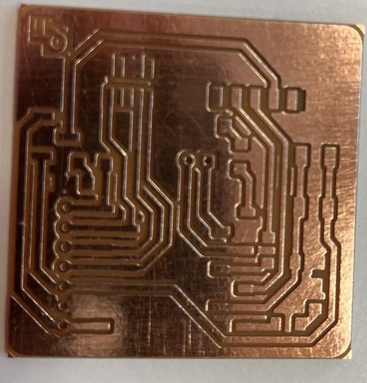
The success of the PCB manufacturing process can be measured by the quality of the final result. In this case, the use of the CNC milling machine has proven to be exceptionally effective, producing a high-quality PCB in an acceptable time. The next phase of the project, soldering components, is equally crucial. The ability to solder accurately will influence the functionality of the circuit.
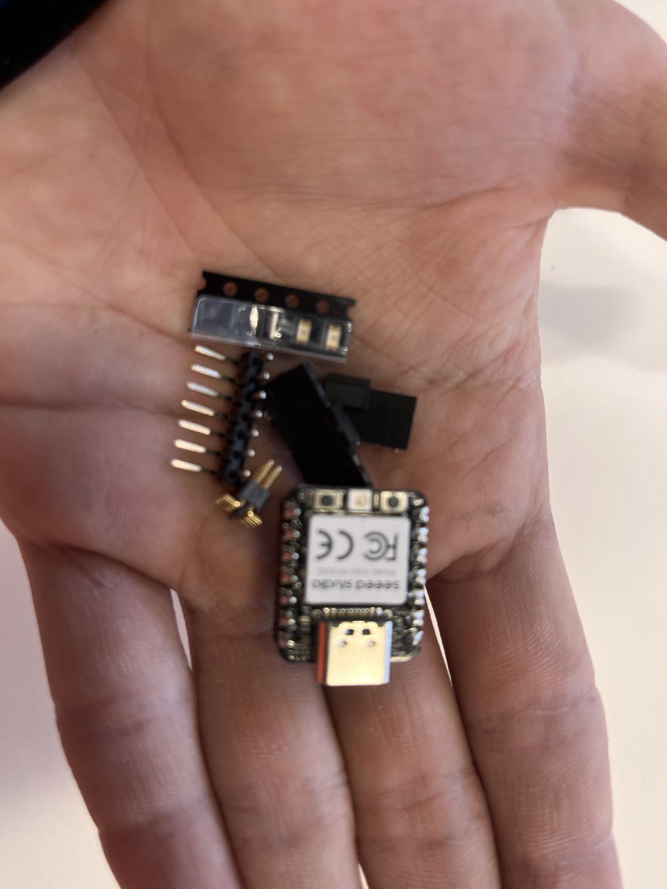
Components to use
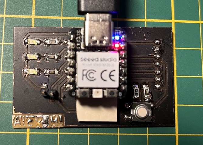
1 SEEED STUDIO XIAO RP2040
1 CONN HEADER SMD 10POS 1.27MM
1 CONN HEADER SMD R/A 6POS 2.54MM
1 Tactile Switch SPST
3 LED 1206 SMD
4 RES 1K OHM 1% 1/4W 1206
1 RES 499 OHM 1% 1/4W 1206
2 CONN HDR 7POS 0.1 TIN SMD
Assembly of components
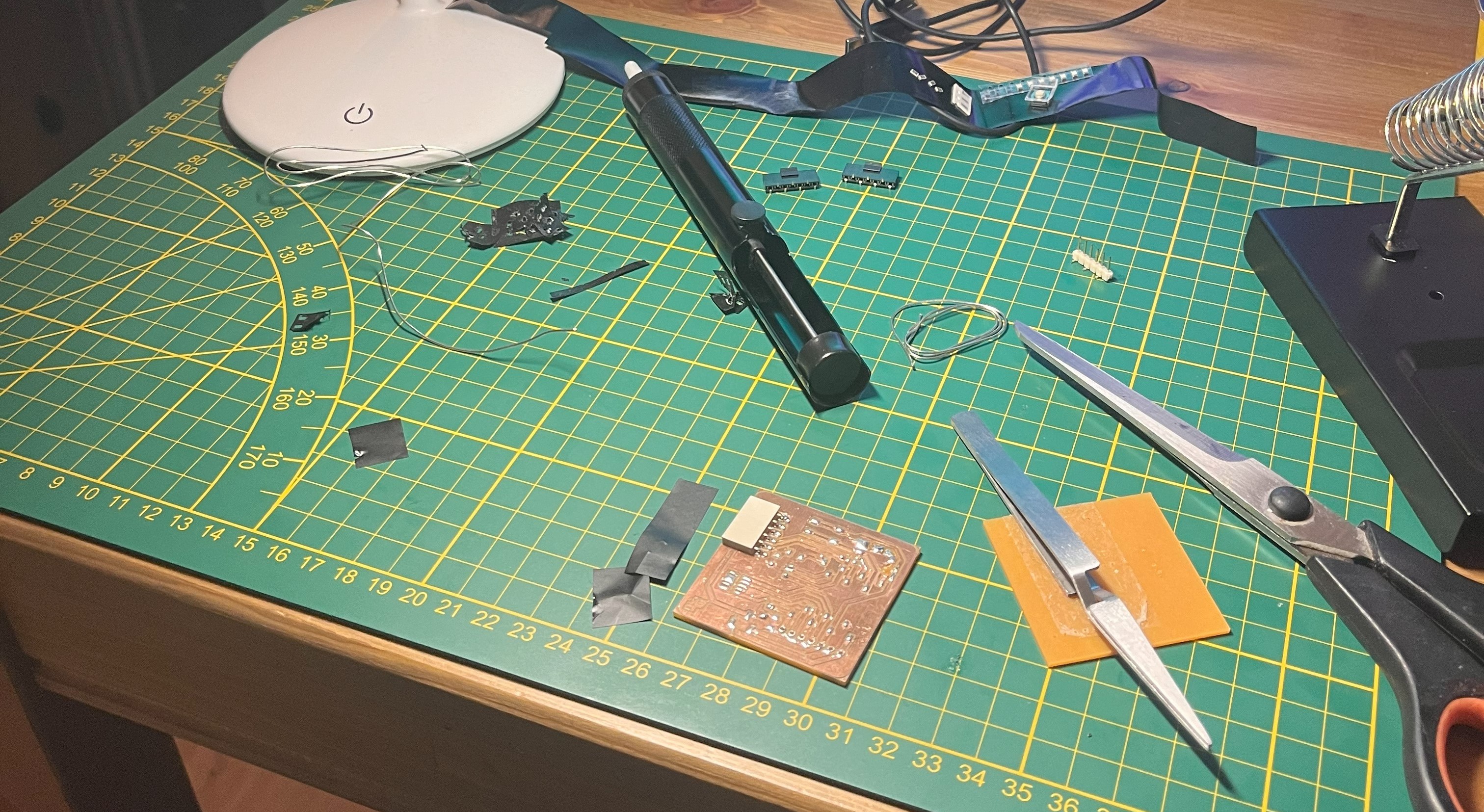
The meticulous task of placing and soldering SMD (Surface Mount Devices) components is a process that requires precision and patience, especially when a solder mask is missing, yet there were no setbacks and the assembly was completed successfully.
Testing my board( Blinking led)
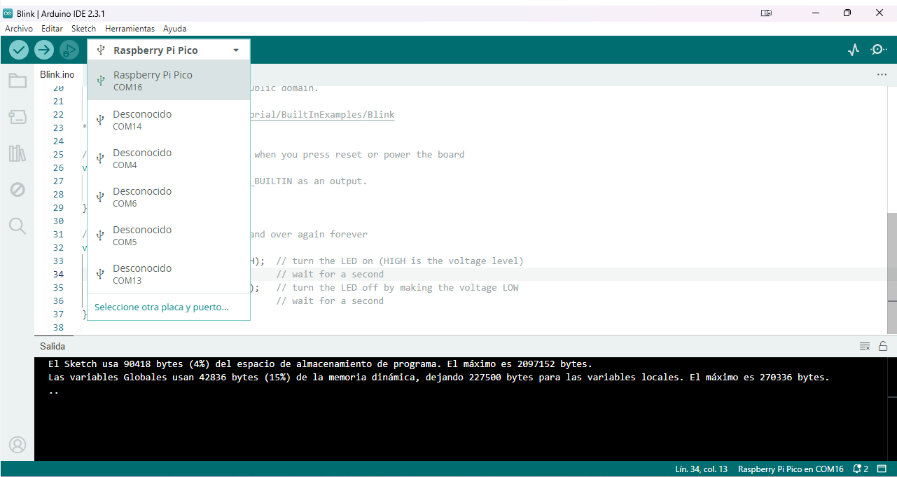
To test the manufactured PCB, using the Arduino IDE Blink example is a great way to verify the basic functionality of the board. This program is essential in the Arduino world, allowing new and experienced users to confirm that their hardware and software are configured correctly.
In order to use the Xiao in the Arduino IDE you must follow the following steps:
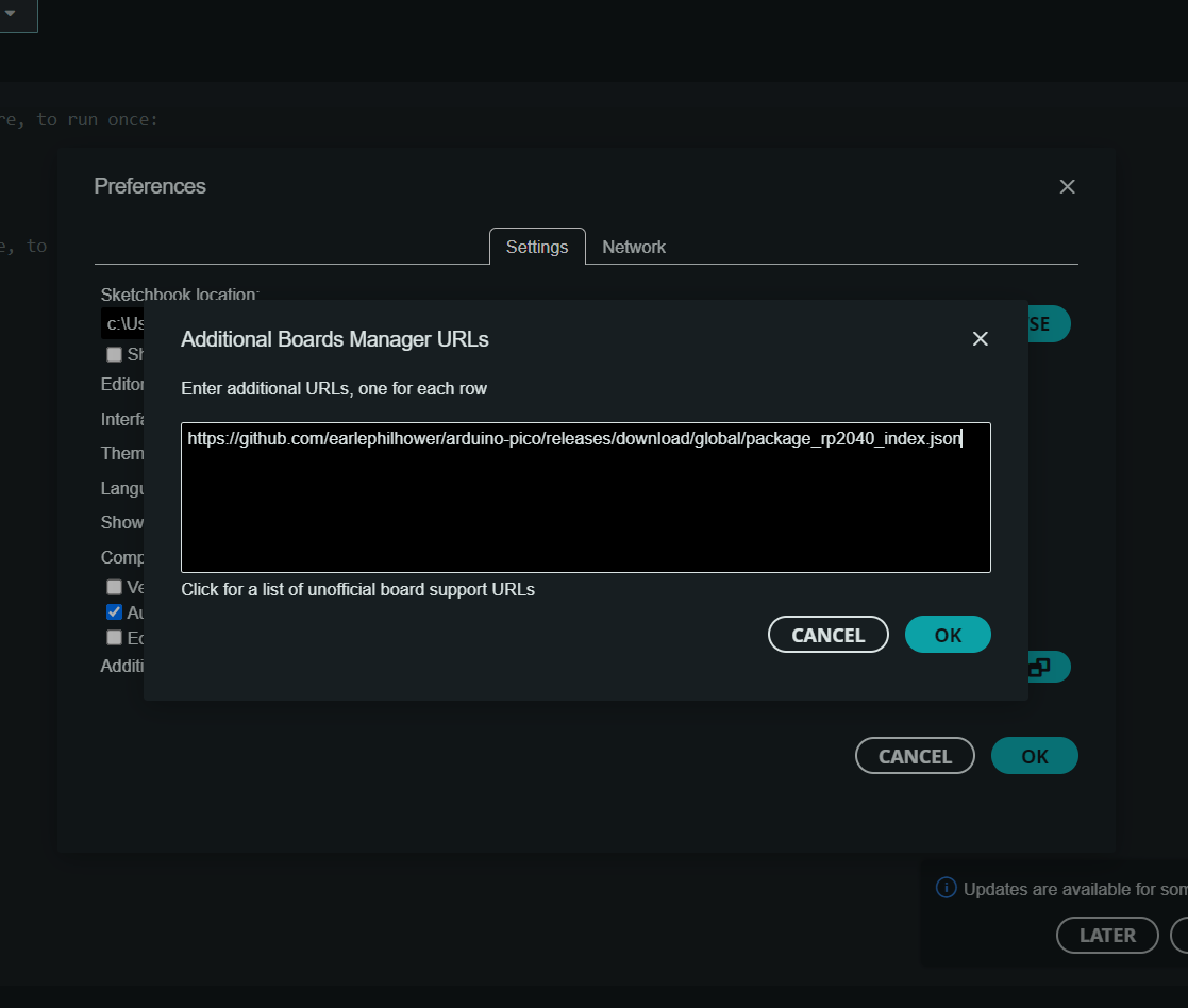
1. Download the arduino app
2. Open the application -> file -> preferences -> add "https://github.com/earlephilhower/arduino-pico/releases/download/global/package_rp2040_index.json" in the "Board Manager additional URLs"
3. Select Tools -> Dashboard -> Dashboard Manager -> search for “pico” and install it.
4. Select file -> examples -> basics -> blink
In this video we can see the final finish of the PCB after the assembly of the components, we can also see the blink program working with a slight change in the frequency of the blinking to give more personality to the test.
Customizing the design
Taking The Quentorres' original design as a starting point, the redesign process led to the creation of a PCB with its own characteristics, distinguished by a different arrangement of components and an altered pin selection.Using Inkscape software, which has been mentioned and used in previous stages, prepare for the application of a solder mask
Well, once we have it in inkscape, we export it to cut into vinyl, and with a lot of patience, we place it at the points where the welding was. This method is very practical when traditional solder mask application methods are not available in PCB manufacturing.To then be painted with a layer of paint that will function as a homemade welding mask.
Applying a layer of solder mask on a PCB has multiple practical and aesthetic benefits. Although the final performance of the circuit may be the same, its presence offers additional protection against oxidation and possible short circuits. This not only improves the durability of the PCB, but also makes component assembly easier, reducing the risk of accidental bridging between nearby traces. Additionally, the solder mask contributes to a cleaner, more professional finish on the PCB. Visually, a soldermask PCB looks more uniform and neat.
Another Method?
Manufacturing PCB prototypes using acid-based solutions is a traditional and economical method, especially suitable for resource-limited environments. This approach involves removing unwanted copper from the board surface through a chemical reaction, leaving only the circuit traces. The accuracy of this method may vary, but it is a valuable technique for rapid prototyping or hobbyist projects. Combining this technique with laser cutting opens up new possibilities. The laser can be used to, after applying a layer of paint, precisely etch the circuit design into the surface, marking the areas that must remain exposed to the acid. The acid solution is then applied to remove the exposed copper, while the areas not affected by the laser remain intact. This combination can significantly improve the accuracy of PCB prototypes manufactured using acid-based methods, while keeping costs relatively low and affordable.
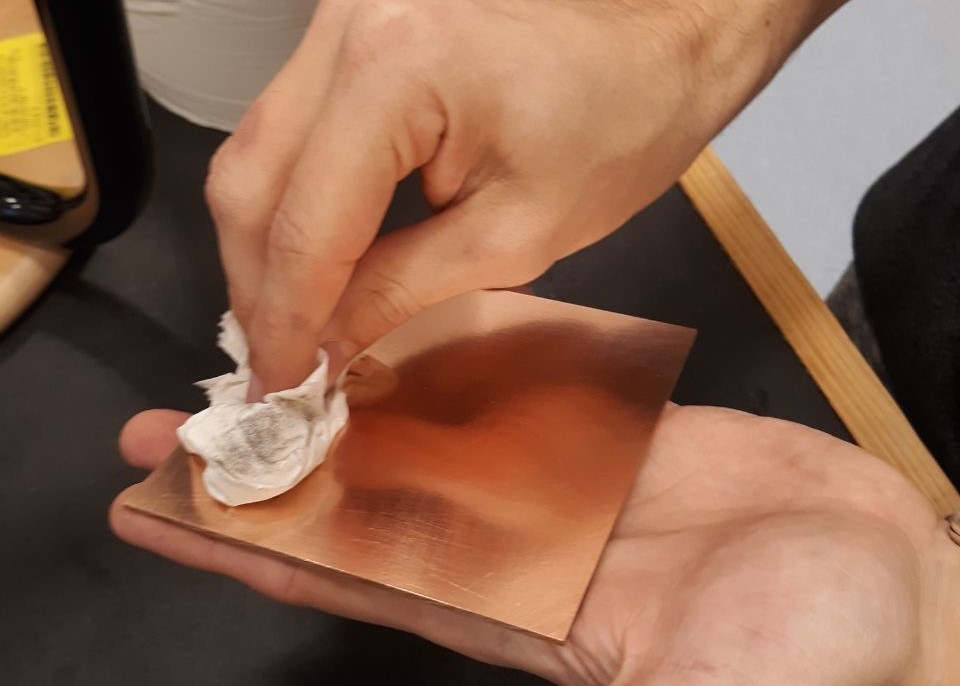
Once we have cleaned the surface of the PCB, first with a copper or aluminum scouring pad and then with alcohol, then with a spray paint of any color (although matte black is ideal) we apply a generous layer of paint on the virgin PCB.
This method is a little more experimental than CNC manufacturing and the parameters will depend on the type of laser, the paint used, the speed of the laser, etc... in my case I had to make several attempts until I got the desired result.
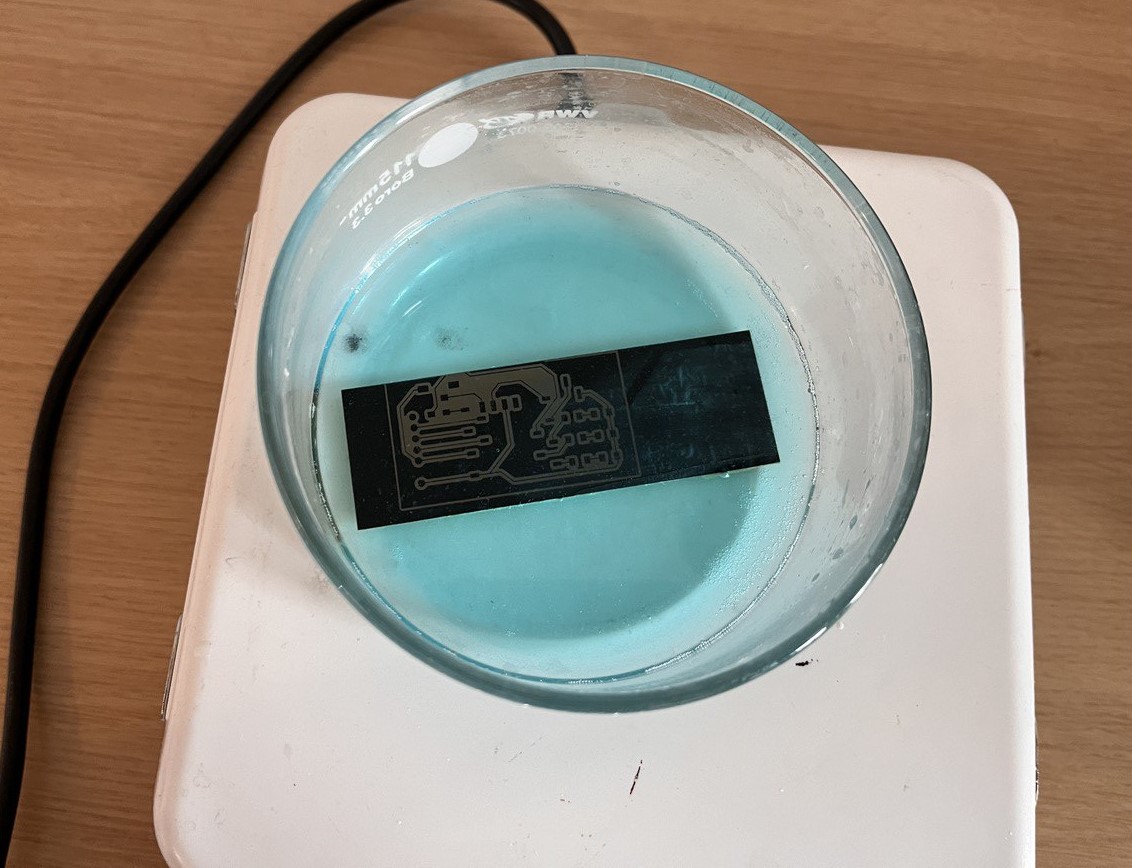
Finally, at the suggestion of my instructor Axel, I use a sodium persulfate solution because it is cleaner than iron perchlorate. In addition, it has the advantage of being transparent (but turns blue when used, so its efficiency can be distinguished by its color).
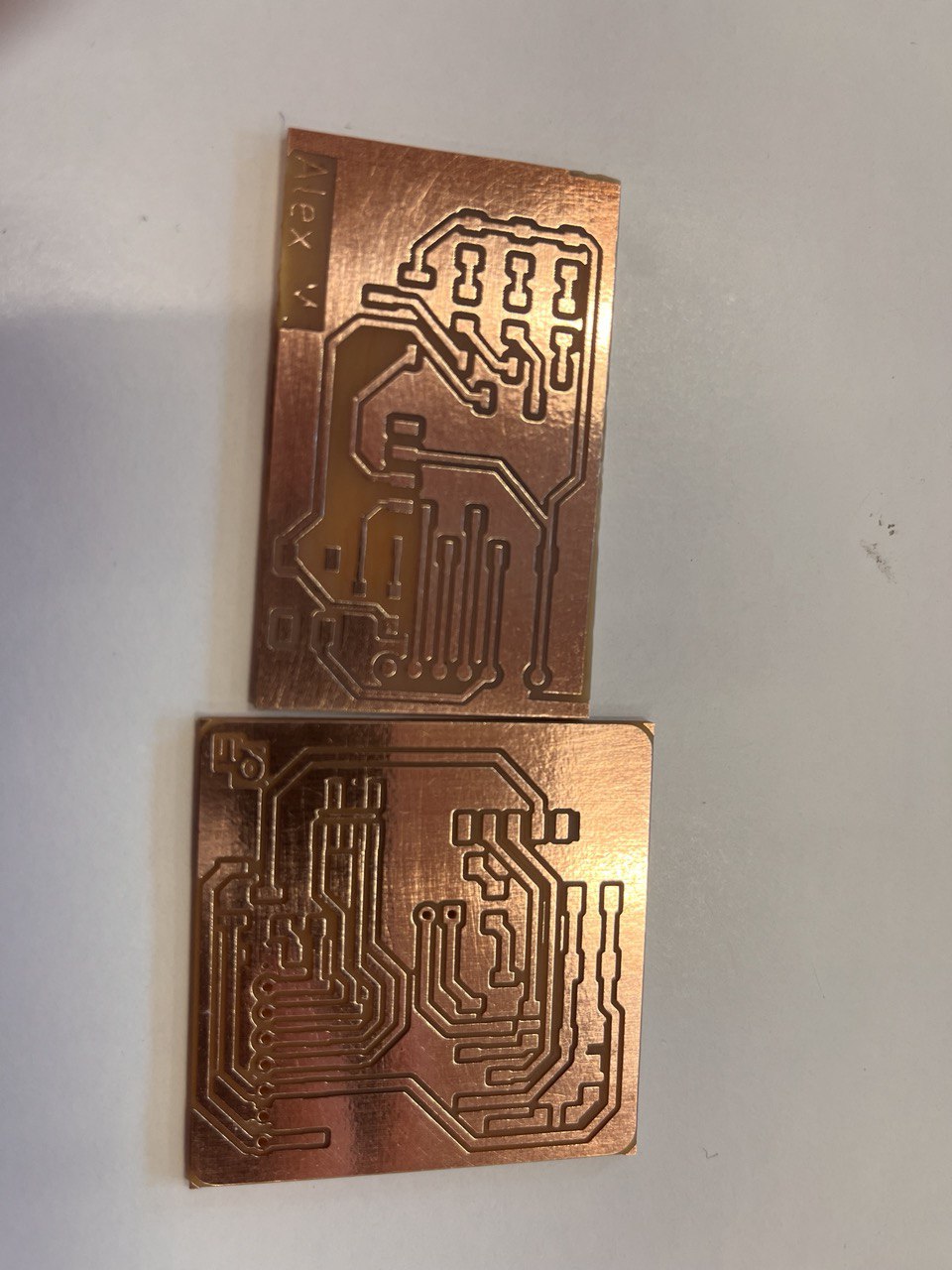
Here we can finally see a PCB made using chemicals and another using CNC, from left to right respectively and there is no difference in quality from one to the other, both were perfect, without lost tracks or dirt between the tracks.