✨🌸Electronic design🌸✨
Hey there sis, welcome to this week's assignment where we're totally learning tall about PCB design and fabrication! Get ready for some really cool pink stuff ahead.
First of all I will explain what PCB fabrication is all about. So, basically, special gorgeous machines that are programmed to do this take our digital designs and turn them into real life circuit boards. It's just like a carving wizzard omg🌟 they use this super fast cutter to carve out pathways on copper boards, making the circuits we need. The minimum trace width on a PCB is like the narrowest path it can take, it is like a little highway for electricity. It's super important because it keeps things from overheating or breaking when carrying current.
And then there's the number of layers lol I like to think of it like building a sandwich! More layers mean more room for cool stuff without making the board bigger. But you gotta find the right balance because it affects how well everything works and how much it costs so be careful, we are not millionaire´s...YET😎💸
✨Massive shoutout to our instructors for their engaging and enlightening session, guiding us toward mastering the art of PCB fabrication here at the FabLab Puebla. With these insights, we're ready to use this tech! Thank you!!🧸
For a better knowledge, feel free to check the Electronic Design week below
⬇️
All about the design💅🏼
- MY Fab academy ✨NETWORKING and COMS WEEK
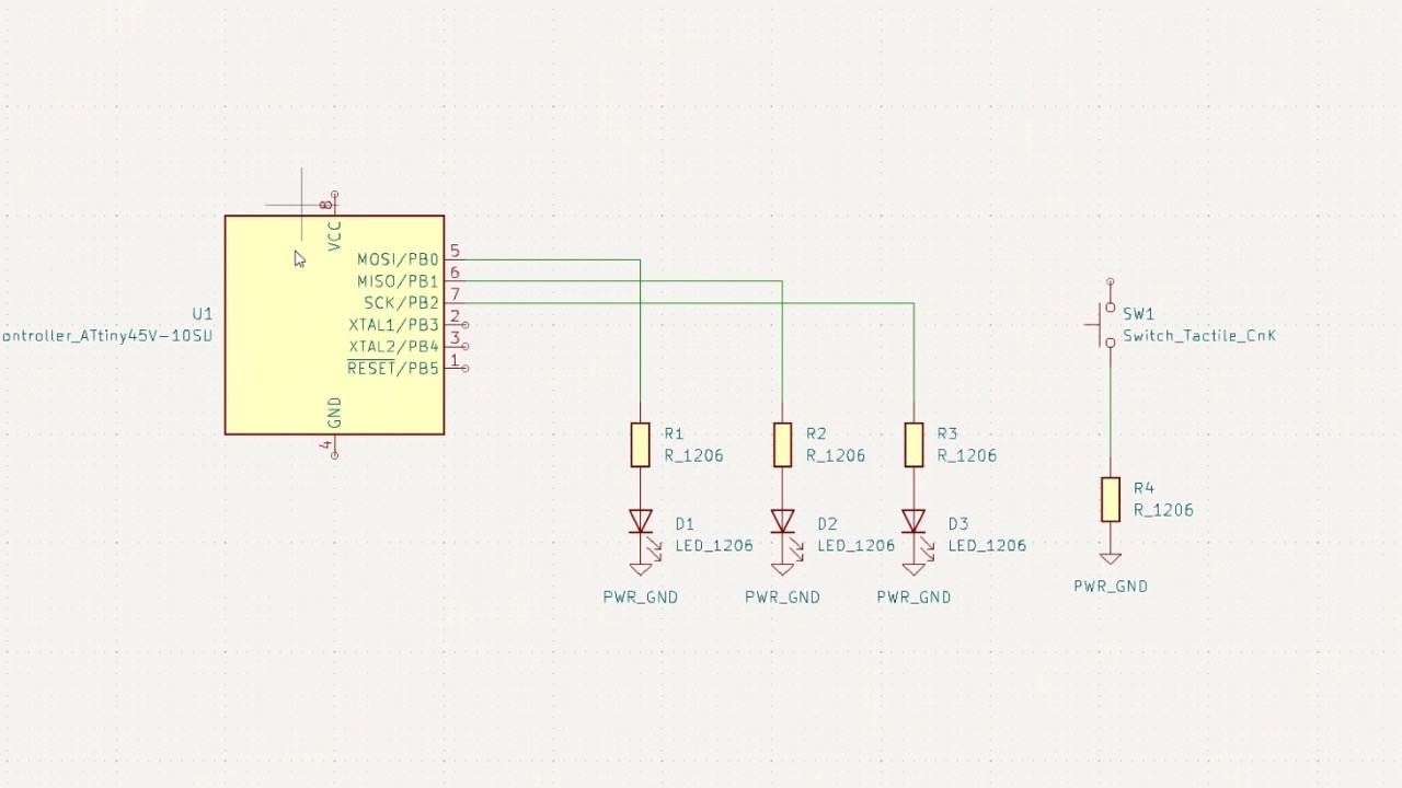
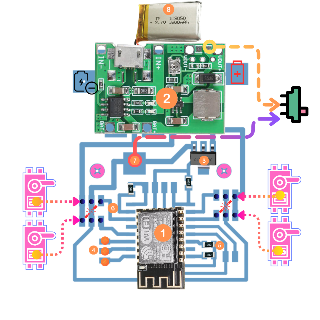
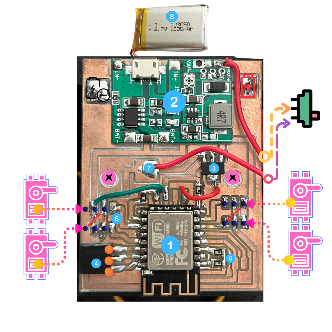
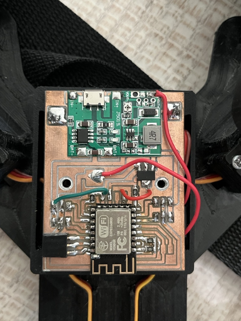
Power Supply Design❥ I connected the 3.7V LiPo battery to the TP4056 charging board with step up❥ Then used the step up output to provide 5V to the servos and 3.3V to the ESP-12-F via the AMS1117 voltage regulator.
Microcontroller❥ First I Powered the ESP-12-F with 3.3V from the AMS1117❥ TIP: You shall connect GPIO pins to control the servos (typically GPIO 12, 13, 14, and 15 for servos 1, 2, 3, and 4 respectively)❥ Finally connect the button to an available GPIO pin to switch modes.
Servos❥ For this part connect the servo signal wires to the corresponding GPIO pins on the ESP-12-F❥ Power the servos with the 5V output from the step up converter.
Microswitch❥ Place SMD capacitors close to the power pins of the ESP-12-F to stabilize the power supply.
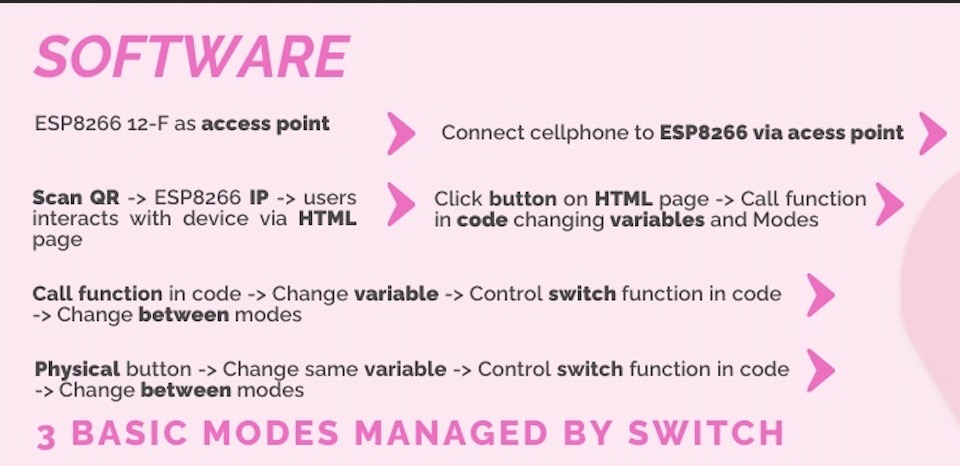
Program❥ Configure the ESP-12-F to act as a WiFi access point. Create an HTML page hosted on the ESP that allows users to control the servos via buttons on the webpage. For this part please go to application + interface week
APP AND INTERFACE ---->
- SOPHIE´S APP AND INTERFACE PINK WEEK
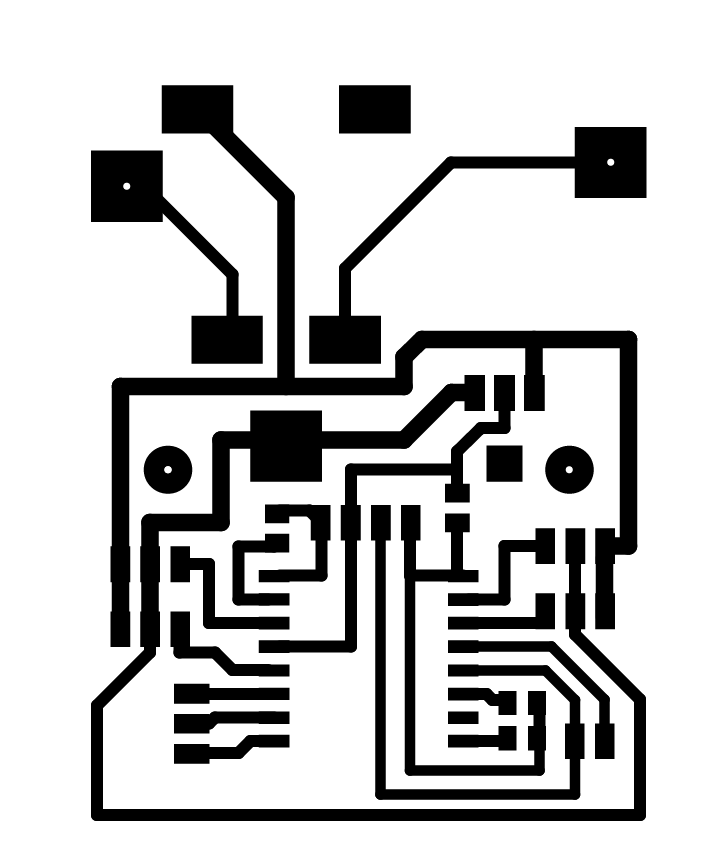
Layout the components❥ First place the ESP-12-F in the center❥ Arrange the voltage regulator, TP4056 board, and capacitors near the power input❥ Position the servos connections along one edge for easy wiring❥ Place the microswitch and button conveniently.
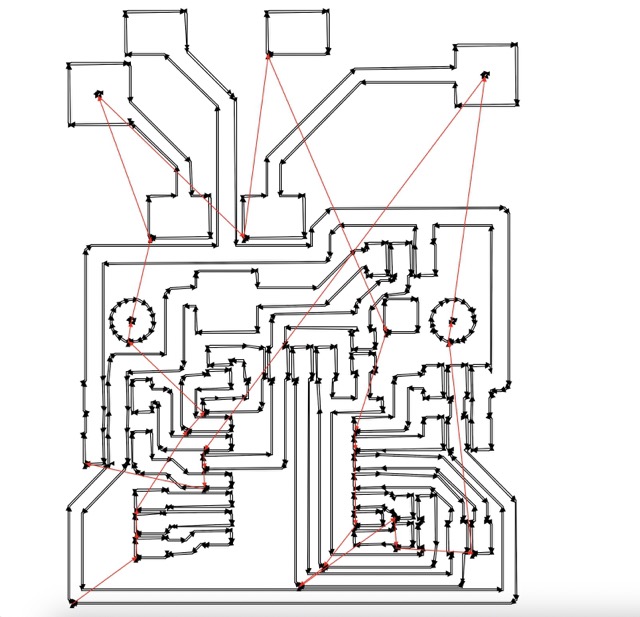
Routing❥ Route power traces to ensure stable supply to all components❥ Ensure signal traces from ESP GPIOs to servos are clean and without interference❥ Follow design rules to ensure minimum trace width and clearance.
- FOR A DEEPER STEPS GUIDE OF ELECTRONIC PRODUCTION PLEASE CLICK HERE WEEK 4💋
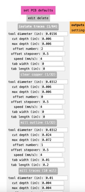
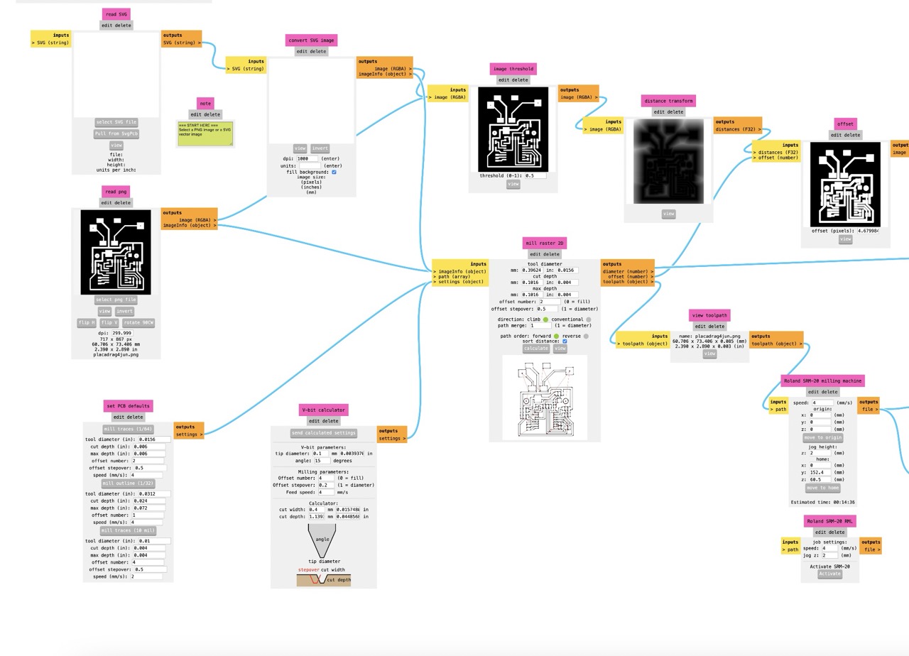
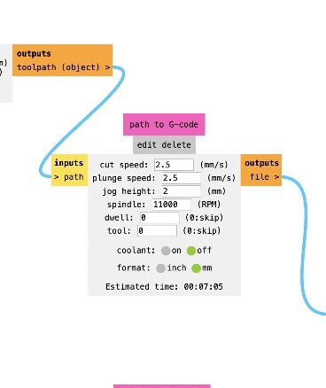
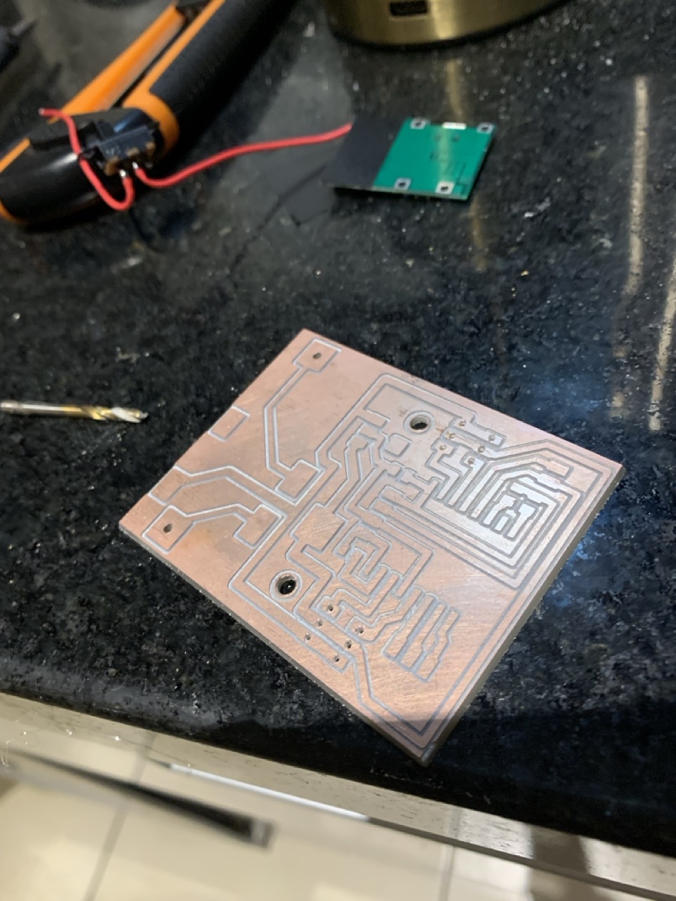
So for the tools, I used a pretty 15-degree V-bit for engraving and a 0.8mm diameter two-flute end mill for cutting. Also I used this cool software called MODS to make things easier. Trust me, it's a bit intimidating at first, but once you get the hang of it, it gets better!🌺
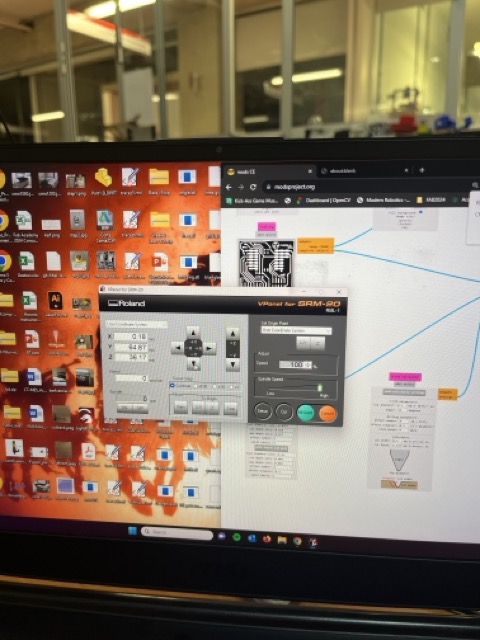
For managing the Roland I used V-carve software to cut.
In V-carve first, I calibrated in x, then in y, and then the z-axis is where we mark our starting point. Then I swapped out the engraving tool for a V-angle one. After I finshed, I did another calibration, but this time just in z, so I could pop in my 0.8 mm diameter cutting tool. Oh, and always remember, when you're putting your tools in the holder, make sure it's not too tight! Gotta leave it loose so we can do that last bit of calibration by hand and make sure it's all perfect. Don't wanna break the tool when it goes down in z, you know girl...? (I DID)

So now u know all bout designing stuff.. are u ready to create ur very own dazzling PCB from scratch using the Roland SRM-20 milling machine? Let’s dive right in! IK hun iknow... You´ll enjoy it later u´ll see´
HOW TO MAKE THIS PCB STEP BY STEP GUIDE
IF YOU WANT TO SEE EVERYTHING ABOUT HOW MY BOARD WORKS PLEASE GO TO MY FINAL PROJECT. HERE I´M JUST GONNA TALK ABOUT IT IN A NUTSHELL. THIS ARE THE SCHEMES THAT SHOW HOW IT WORKS. AND THAT´S JUST ALL I´M BOUT TO TALK HERE CUZ´THIS WEEK IS ELECTRONIC DESIGN 4 A REASON HUN.
- MY FINAL PROJECT💋
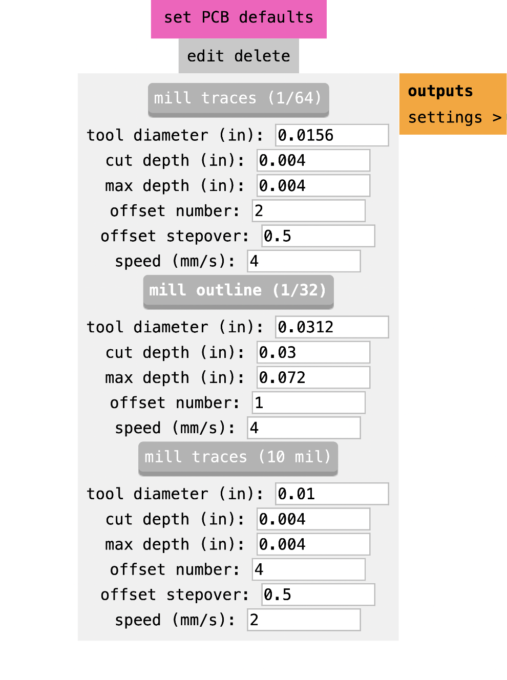
- 🌸For engraving, use a 15-degree V-bit. This tool is perfect for creating fine details and precise engravings on your copper board. The sharp angle allows for delicate cuts without damaging the board.
- 🌸For cutting, use a 0.8mm diameter two-flute end mill. This bit is great for making smooth and accurate cuts. The two flutes help to remove material efficiently and prevent clogging, ensuring clean edges.
For X-Y calibration move the spindle to the starting position (home position) for the x and y axes. This ensures your design is milled in the correct location on the board.
For Z calibration lower the spindle to the surface of the copper board to set the z-axis zero point. This ensures the engraving and cutting depths are accurate.
Spindle Speed: 10,000 RPM
Feed Rate: 100 mm/min
Depth of Cut: 0.1 mm
These parameters are important because the high spindle speed and moderate feed rate allow for precise and clean engraving without damaging the copper. The shallow depth ensures that only the top layer is removed, creating fine details. Begin the engraving and once it’s completed, switch to the cutting tool and start the cutting process. Always monitor the machine to ensure everything is running smoothly.
🌸 Make sure the footprints of your components match the pads on your PCB. This includes checking the pin spacing, pad sizes, and overall dimensions.
🌸 Ensure there's enough space between components to avoid short circuits and to make soldering easier.
🌸 Use the DRC feature in KiCad or PCB wizard to check for any design rule violations. This will highlight issues like minimum trace width, clearance, and pad sizes.
🌸 Ensure that all layers (top layer, bottom layer, silkscreen, solder mask) are correctly defined in your design. Make sure your copper traces are on the correct layers.
🌸 Add a ground plane to reduce noise and improve signal integrity. This is usually done on the bottom layer or as a separate internal layer.
🌸 Verify that your trace widths meet the minimum requirements for your fabrication process. For standard processes, a 6 mil (0.15 mm) trace width is common.
🌸 Ensure that there is enough clearance between traces and pads. A typical minimum clearance is 6 mil (0.15 mm).
🌸 Make sure vias are of appropriate sizes. Typical via sizes are around 0.3 mm for the drill hole and 0.6 mm for the pad.
🌸 Ensure that the silkscreen layer is legible and doesn’t overlap with pads or traces. This will help during assembly and debugging.
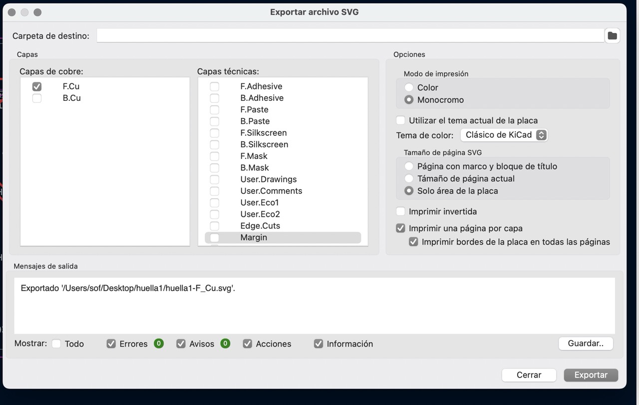
🌸 Generate Gerber files for all layers. This includes copper layers, silkscreen, solder mask, and the drill file. Ensure the files are named according to your fabricator's requirements so you are not taking any chance for mistakes.
🌸 Create a detailed list of all components, their footprints, and quantities. Ensure all components are available and can be sourced.
🌸 If you’re producing multiple boards, consider panelizing them. This can make the manufacturing process more efficient.
First off, I downloaded KiCad, this awesome platform our instructors recommended for designing electronic PCBs. I kicked things off with a tutorial from my fab lab advisor in Puebla. He showed me how to design a custom Arduino like controller for my Xiao board and we downloaded together all the libraries my KiCad needed. This was my first time using KiCad and we started things off designing this board, easy peasy.
Soooo getting back to the deal… when I was designing the board, I made sure to include resistors for each LED and component output. Plus, I wanted to add pins to make it more versatile. Here's what I used:
When you're about to export the margin, you should check the boxes for 'margin' and 'user drawings', remove them for the paths. Remember, before saving, verify that the paths you create are preferably the width of your tool, in my case it was 0.4 millimeters, and that's how I reset it from the beginning.
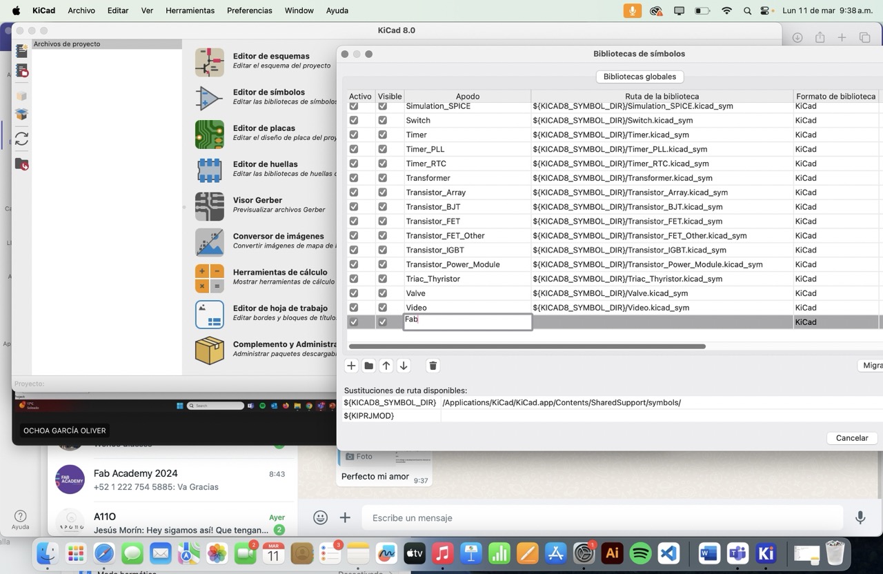
So the T´ honey bee.. including libraries in KiCad is super important, It gives you access to a fabulous array of pre designed symbols and footprints, making your design process a breeze. To include them, open KiCad, go to Preferences, and manage your libraries in both the Symbol and Footprint Editors. Adding libraries ensures you use accurate, industry standard components, saving time and reducing errors. Custom libraries let you create and reuse your unique components, adding that personal touch. Shared libraries are perfect for team projects, ensuring everyone’s on the same page. I downloaded mine from fab academy git library. With everything in one place, your workflow will be efficient and accurate.
My pretty design for this week it´s going to be my final´s project board and how I physically designed all of my boards since I did them all by myself and I really really like to show them off.
ALSO I KNOW I TALKED NICE STUFF OF KICAD BUT FOR ANY OF THIS BOARDS I USED IT. WHY? CUZ MY TEACHERS TOTALLY SHOWED ME HOW TO KICK IT OFF BUT TBH IT´S NOT MY STYLE. I WANT TO DRAW IT OLD SCHOOL AND PCB WIZARD SOFTWARE WAS BY BESTIE IN ALL OF THIS SITUATION. I HIGHLY RECOMMEND IT BUT THAT´S JUST MY OPINION SWEETIE.
Personally, I was itching to use ferric chloride because it's way quicker, plus the Roland machine was booked 24/7 :( but I ended using the Roland SRM-20 and V-carve software to mill my boards. Obviously I used for all of this MODS software cuz´DUH girl it is the best.
So how did u came for your final project✨ board design hun?
For the electronic production🌸✨
So, for the design I had to take in consideration that i was going to program this board with a CH340 plug. The CH340 acts as a bridge between your computer (via USB) and the ESP8266 microcontroller, so when you upload code or send commands from your computer, the CH340 converts these signals into UART serial data. This data is transmitted (TX) to the ESP8266, which receives (RX) and processes it similarly, responses or data from the ESP8266 are transmitted back to the CH340 via UART, then the CH340 then converts this data back into a format understandable by your computer.
IN A NUTSHELL----> I used UART protocol, which allows for bidirectional communication, enabling you to program the ESP8266 and control the relay board remotely. It's essential for uploading code, debugging, and sending/receiving data between your computer and the ESP8266 board. Ensure baud rate settings (typically 115200 or 9600 bps) are consistent between the CH340 and ESP8266 for reliable communication.
TO SEE ALL ABOUT THIS FABULOUS 🎀BOARD🎀 AND HOW IT WORKS PLEASE GO TO
How to make the electronics work PLEAAAASE GURL
So, here's how I made this whole ESP8266 12-F setup work, all while figuring out electronics for the not so first time but ish...
☻Small summary☻
Always always always check all connections twice before powering up. Use a multimeter to verify voltages. Debug with serial output to ensure the ESP is responding correctly to commands.
ELECTRONICS PRODUCTION
TO SEE ALL THE STEPS TAKING IN CONSIDERATION FOR ELETRONICS PRODUCTION PLEASE GO TO WEEK 4. HERE IS EVERYTHING TO SET UP PERFECTLY EVERYTHING. I FOLLOWED THE SAME STEPS HERE HUN.
This were my beautiful parameters:
WHY ARE THE PARAMETERS IMPORTANT? WELL... The spindle speed determines how fast the cutting tool rotates. Higher speeds are great for engraving fine details, while slightly lower speeds are better for cutting to avoid overheating and tool wear ❊→ ❊→ The feed rate is the speed at which the tool moves across the material. A moderate feed rate ensures precision without sacrificing speed ❊→ The depth of cut moderates how deep the tool cuts into the material per pass. Shallow depths for engraving prevent damage to fine details, while moderate depths for cutting ensure efficient material removal without overloading the tool. Obviously by following these steps and using the correct parameters, you’ll create a beautiful, PCB hun. Happy milling🌸✨
HOW CAN I ENSURE MY FABRICATION IS READY?✨🌸
To ensure your board with all of ur components can be fabricated perfectly, you need to follow a few key steps from design to inspection. Here’s a super cute and detailed guide to making sure everything is perffff:
Super important girl cuz we all make mistakes... always have someone else review your design. A fresh set of eyes can catch errors you might have missed.
MY PROCESS OF WEEKS IN A NUTSHELL--->
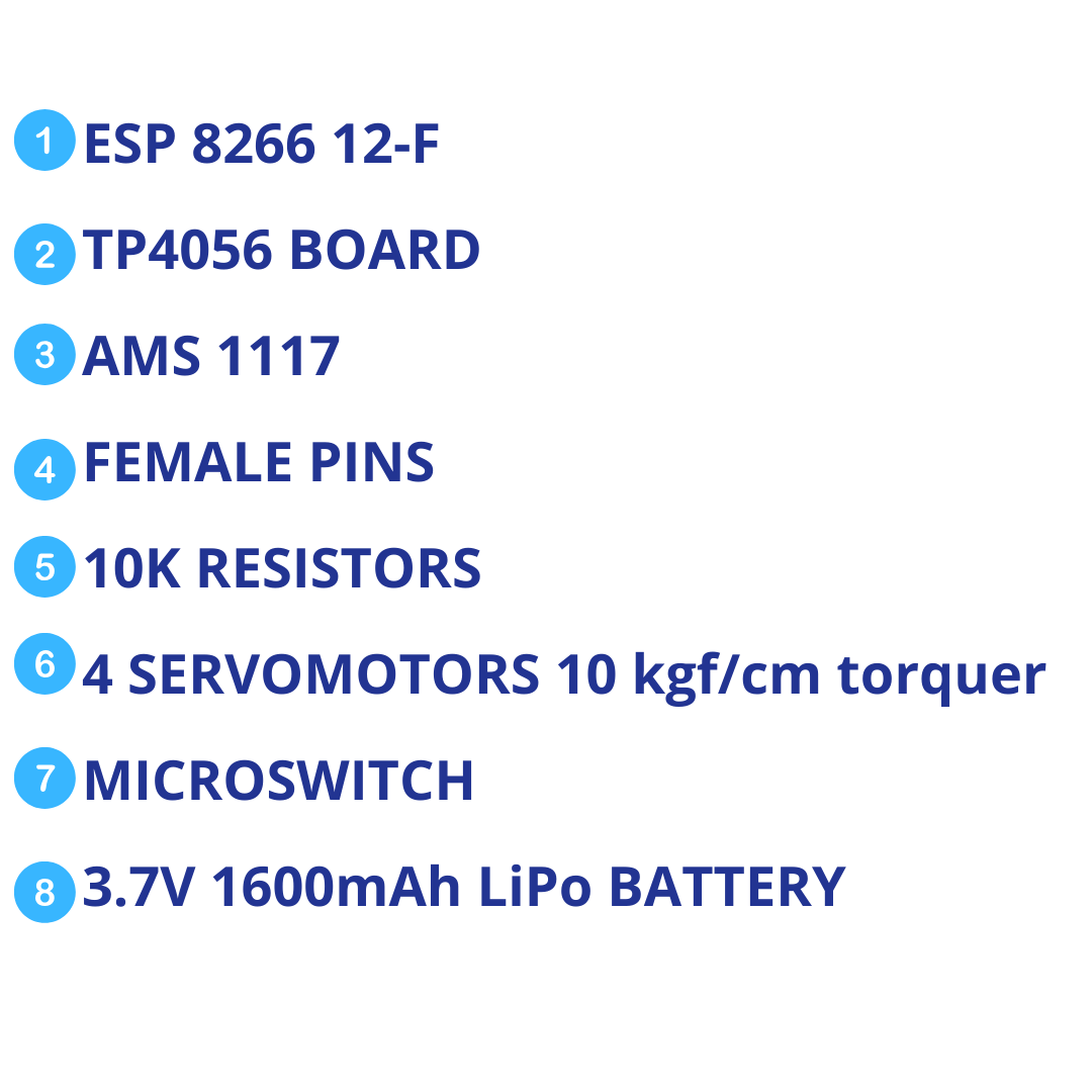
ALL THE components🎀 I USED
🎀And now... my pretty table of components🎀
SOPHIE´S FABULOUS SHOWSACK COMPONENTS |
Where to buy? | Amount | Price | Total price |
| AMS1117 3.3V | Digikey | 1 | $12.80 MXN/unit | $12.80 MXN |
| ESP-12-F | Mercado Libre | 1 | $90.00 MXN/unit | $90 MXN |
| Microswitch 1 pole 2 throws 2 positions | Steren | 1 | $5.00 MXN/unit | $5.00 MXN |
| SMD capacitor 1206 10kΩ | Yageo | 4 | $37.00 MXN/unit | $24.66 MXN |
| Servomotor with 10 kgf/cm torquer | Steren | 4 | $174.00 MXN/unit | $696.00 MXN |
| 3.7V 1600mAh LiPo battery | Amazon | 1 | $183.86 MXN/unit | $183.86 MXN |
| TP4056 board with step-up | Mercado Libre | 1 | $69.00 MXN/unit | $69.00 MXN |
| Copper plate | Mercado Libre | 1 | $90.00 MXN/unit | $12.85 MXN |
| Button | Unit electronics | 1 | $4.00 MXN/unit | $4.00 MXN |
| Total cost | $1098.17 MXN |
MY FINAL CODE:
What I´ve learned so far?
✨🌸From electronic design´s week, I've learned to create precise PCB layouts, select and place components accurately, and ensure proper trace width and clearance. I´ve totally mastered using design rules checks hun (DRC) and generating Gerber files for manufacturing, also I finally understood the importance of ground planes, via sizes, and silkscreen legibility. Additionally, I appreciated the necessity of prototyping, peer review, and communicating with manufacturers for flawless fabrication🌸✨ I KNOW IT WAS NOT EASY BUT IT WAS WORTH IT.