My final project
 March 8, 2024
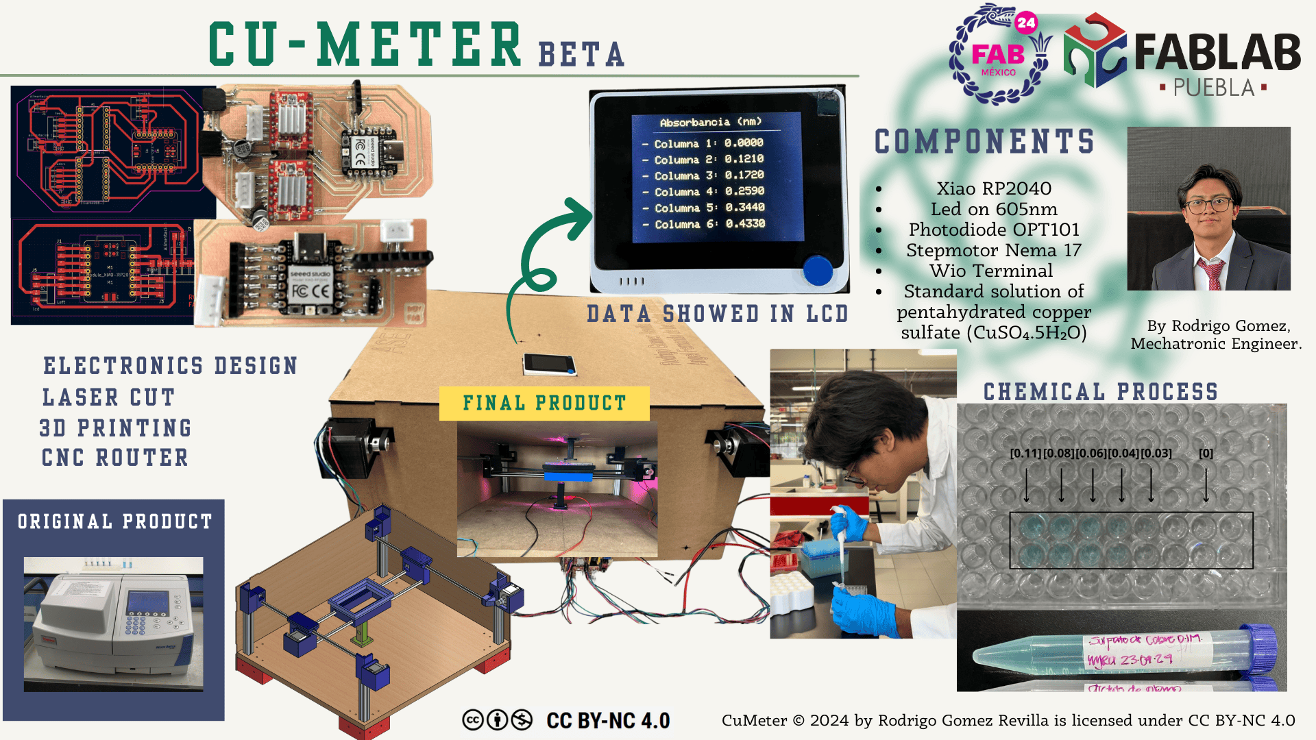
In Mexico, it has been identified that the pollutants we are most exposed to are heavy metals, with the most abundant and toxic being mercury, arsenic, lead, and chromium. One of the main sources of exposure is through clay utensils and their glazes, as these items contain a high percentage of various heavy metal compounds. In response to this issue, a microplate reader was developed for the quantitative detection of heavy metals, with copper as the case study. For its development, the operation of an atomic absorption spectrometer was analyzed, and the mechanism was designed and modeled in SolidWorks to prepare the necessary mechanical parts for assembly. Subsequently, the device was programmed using the Wio Terminal microcontroller to read samples of Copper Sulfate. The developed code enables the reading of each sample in a programmed time of 3 seconds. Finally, the standardization of copper quantification in the samples was carried out, and the results were displayed on the LCD screen of the microcontroller. Twelve tests of 300 µL were conducted to quantify the copper in each sample, and absolute presence was determined in two of them using the device's methodological process. The creation of a microplate reader for the quantitative detection of heavy metals is an economical solution for detecting heavy metals in compliance with the NOM-AA-66-1981 standard.
A lead detector is designed to identify the presence of lead, a toxic heavy metal, in water or mud samples.
Lead contamination poses severe health risks, especially when consumed through water or mud. It can lead to various health issues, particularly affecting children and pregnant women.
I will choose between one of the several electrochemical techniques for lead detection and decidind which can be more accurated to my project i will develop the mechanism to implement with my pcb
In addition to water, some detectors are equipped to analyze lead content in mud. This is particularly relevant in rural areas in Mexico, why? .
In many towns of Mexico its very common to use a lot of dishes made by Mud, its very easy and cheap to do it, so for most of the families are the best option to use it with their food. The main problem its that when the people made this dishes in the process, when the mud burns in the oven, it acquires lead so the families who has these kind of dishes in their daily life with the time past most of them, mainly the children are affected with many cardiovascular diseases and high chances of cancer.
Mid Term Review
April 6, 2024Checklist
-
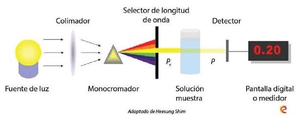
- Light Source: The spectrophotometer starts by emitting light, often in different colors (wavelengths).
- Sample Holder: The light passes through the sample, which could be a liquid, gas, or solid.
- Detector: A sensor measures the amount of light that comes out the other side.
- Result: The machine calculates how much light was absorbed by the sample. Each substance absorbs light differently, like a fingerprint, so this helps identify it or measure its concentration.
My researh
Heavy metals, naturally occurring toxic elements in the Earth's crust, have become significant environmental pollutants due to their widespread use, posing serious public health issues worldwide. In Mexico, glazed clay pottery such as plates, pots, and jars often contains heavy metals like lead and cadmium, which can leach into food and beverages. Despite regulations like NOM-004-SSA1-2013 that discourage the use of heavy metals in utilitarian pottery, many artisans still use these substances due to economic and technical advantages, such as lower firing temperatures and reduced fuel consumption.
The majority of Mexican pottery is fired at low temperatures (850–1000 °C), preventing the formation of insoluble heavy metal compounds and increasing the risk of leaching. This practice is prevalent in low-income communities but is also traditionally used by higher-income households. Lead exposure, primarily through glazed pottery, has been linked to significant health issues, including reduced IQ in children. Studies estimate that children in potter families could lose an average of 7.1 to 8.84 IQ points, with approximately 6,436 children under eight at risk in Mexico.
Detection methods for heavy metals, such as atomic absorption spectrophotometry, anodic stripping voltammetry, and rapid test kits, are often inaccessible due to high costs and the need for specialized infrastructure and expertise. Consequently, affordable solutions for detecting heavy metal contamination in pottery are urgently needed to address this public health concern.
What is a Spectrophotometer?
A spectrophotometer is a scientific instrument used to measure how much light a substance absorbs. It works by shining light through a sample and detecting how much of that light is absorbed or passes through. The amount of light absorbed helps identify the substance and how much of it is present.
 How Does It Work?
Example
If you want to know how much copper is in a water sample, the spectrophotometer can detect how much light the sample absorbs and use that information to calculate the copper concentration. It's like a tool for "seeing" substances that are invisible to our eyes!
I took inspiration for this project because, over the past few months, I completed my social service at an organization dedicated to helping communities involved in the production of clay pottery. In these communities, it was very common to use lead oxide in the process to give the pieces a shiny finish. Even when they didn’t use this chemical, there were cases where they bought clay from nearby towns, which was contaminated with lead due to various factors during its extraction.
From this experience, I began developing the idea of how to identify this heavy metal. During my research, I discovered many chemical characteristics of lead that made its quantification or even simple detection quite challenging. As a result, I decided to focus my final project on the quantification of copper, another element in the heavy metals family.
Why copper and not lead?
Lead has an absorption wavelength below 400 nm, which makes finding sensors that work at that frequency much more expensive. On the other hand, copper has an absorption wavelength around 680 nm, which is within the visible spectrum, making it easier for me to acquire LEDs and sensors that operate at that wavelength.
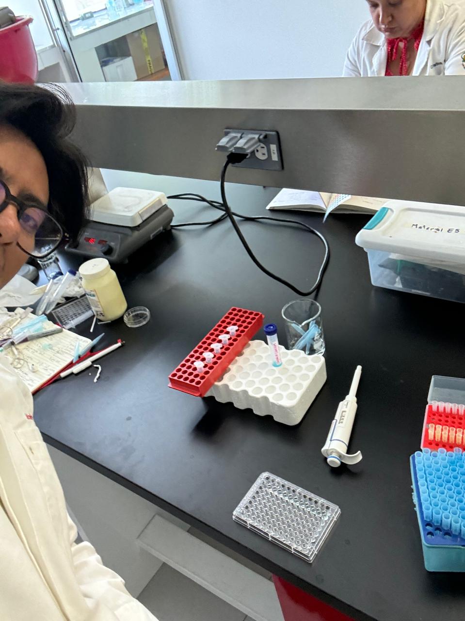
So, I started researching more about how a spectrophotometer works in my university's chemistry lab. I also evaluated different materials using this equipment and later compared the results.
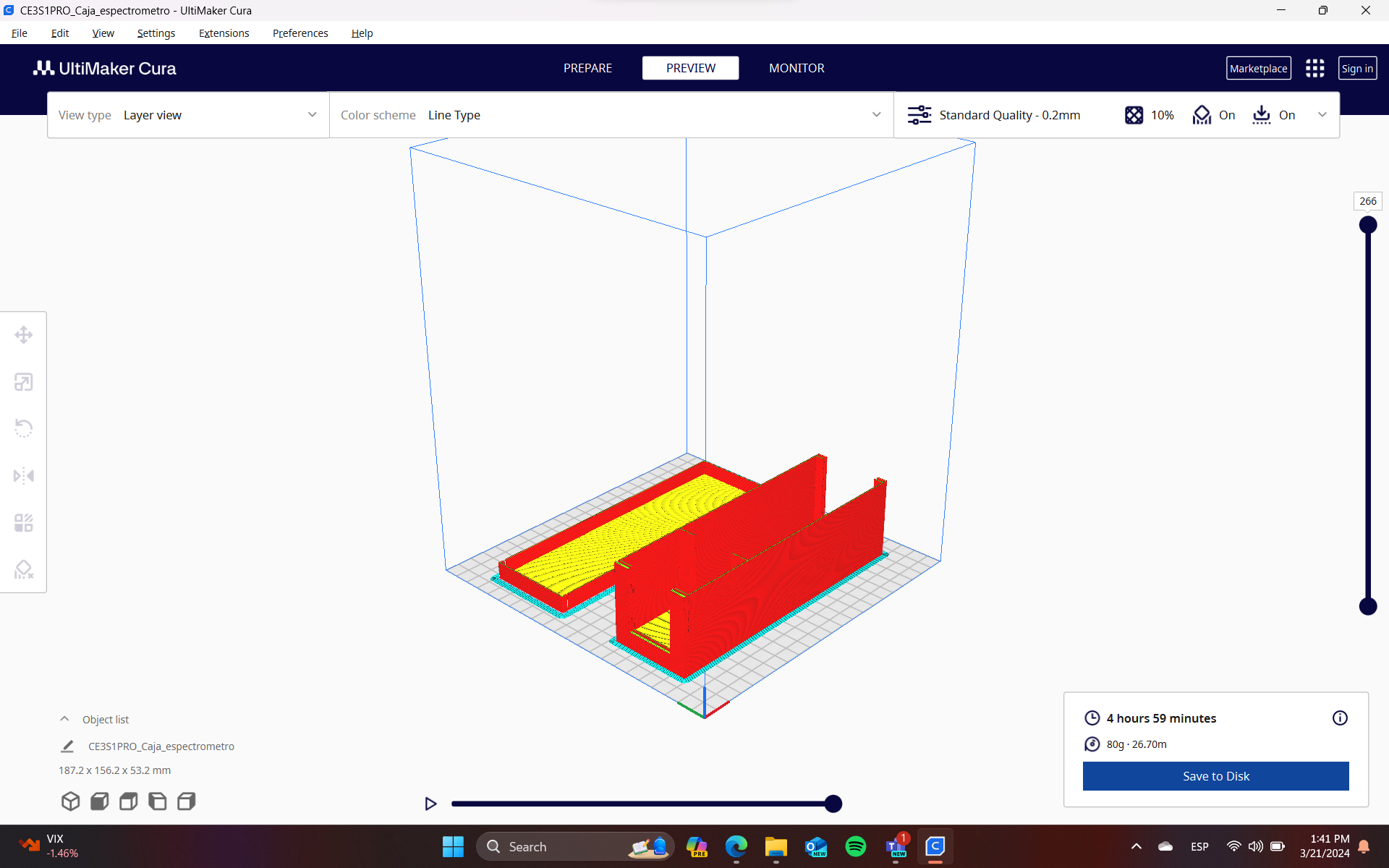
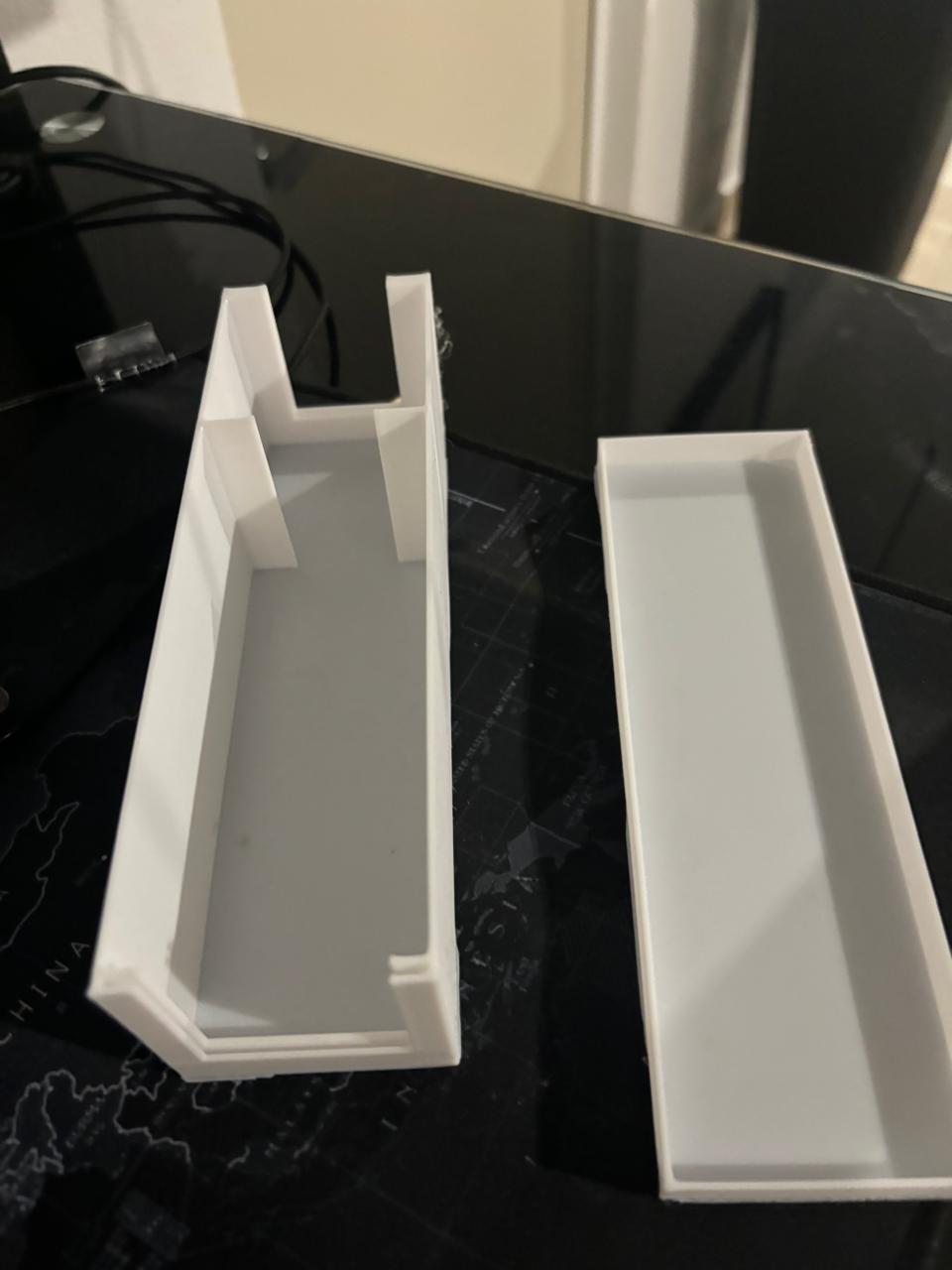
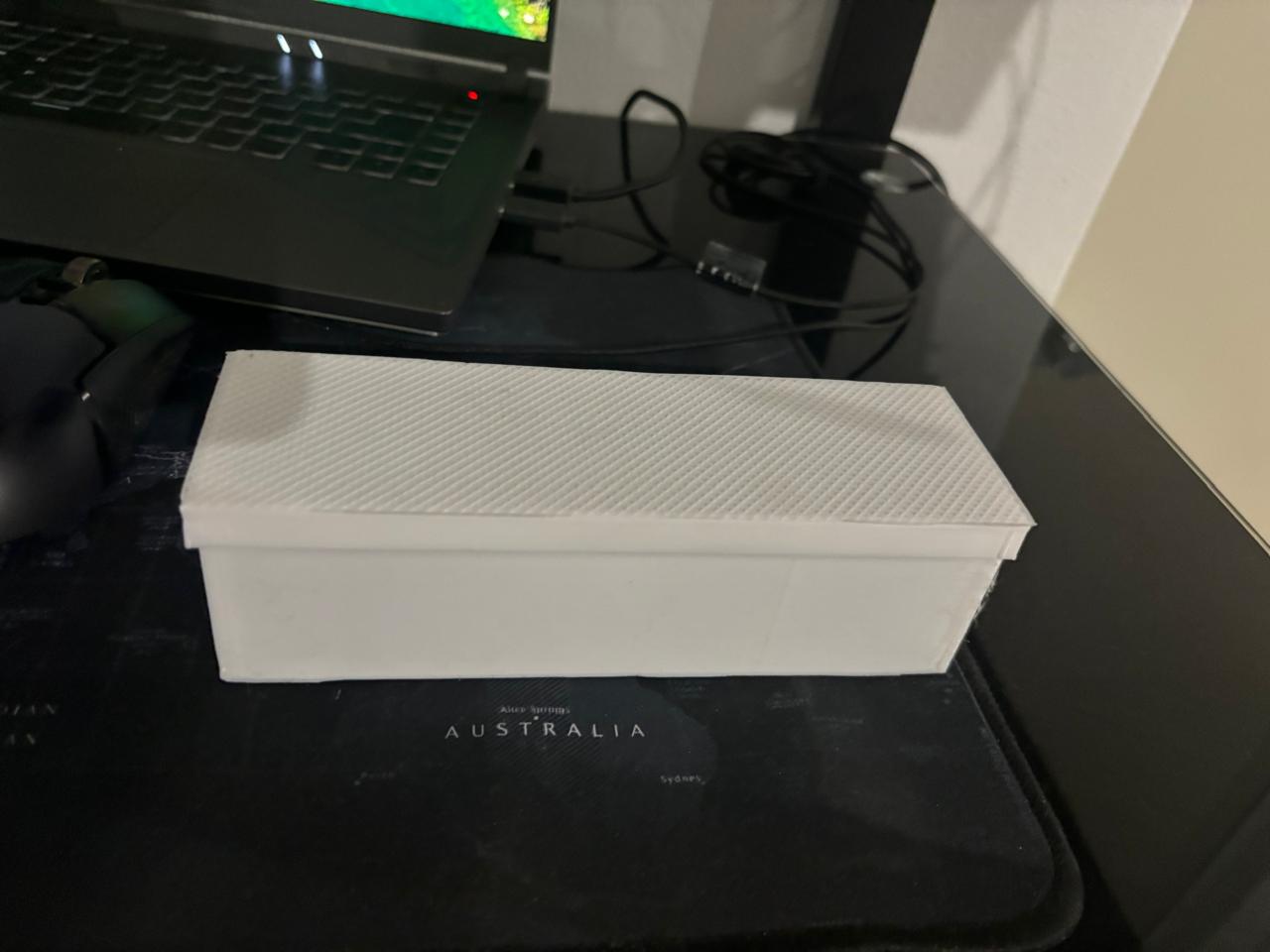
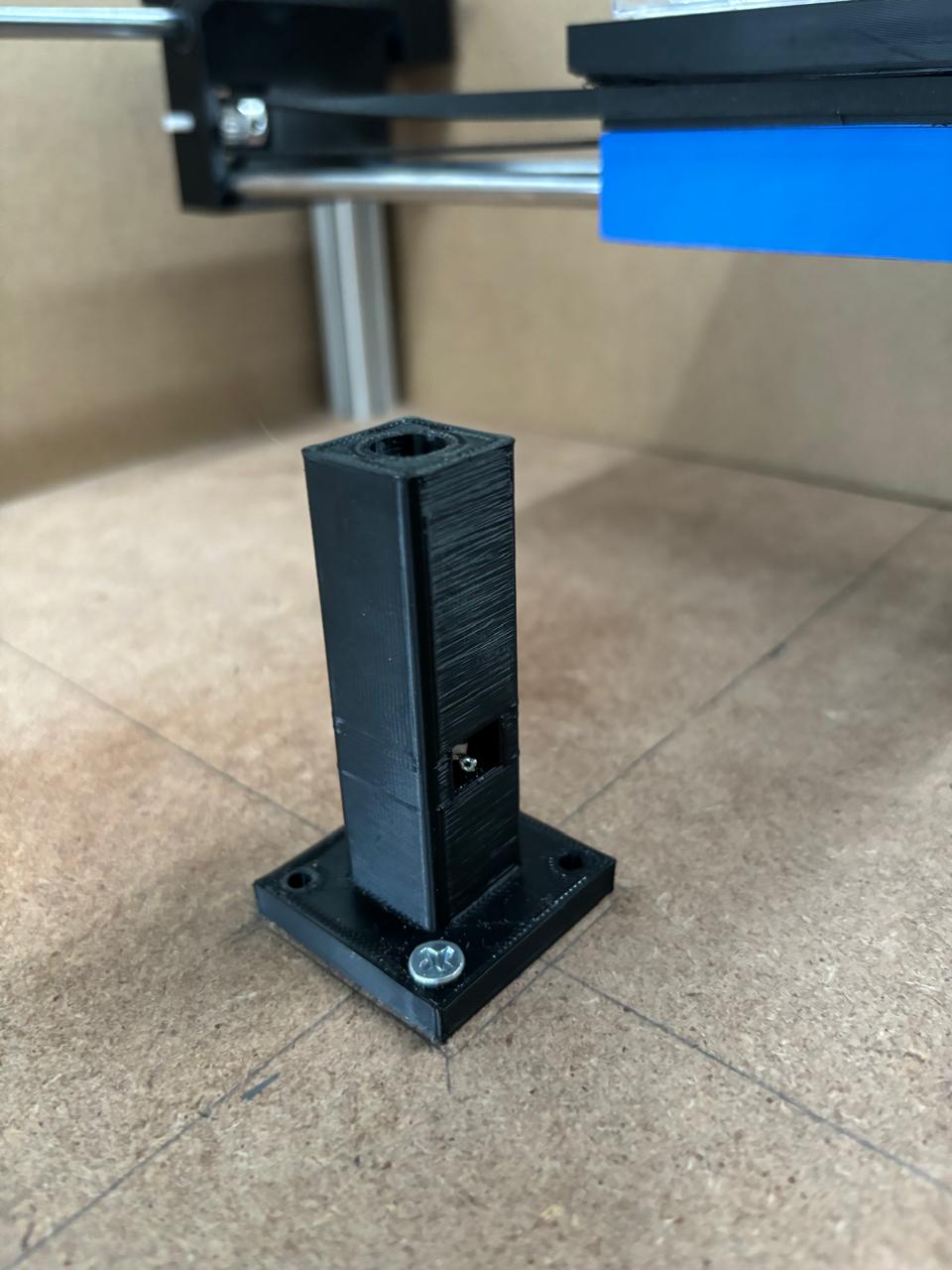
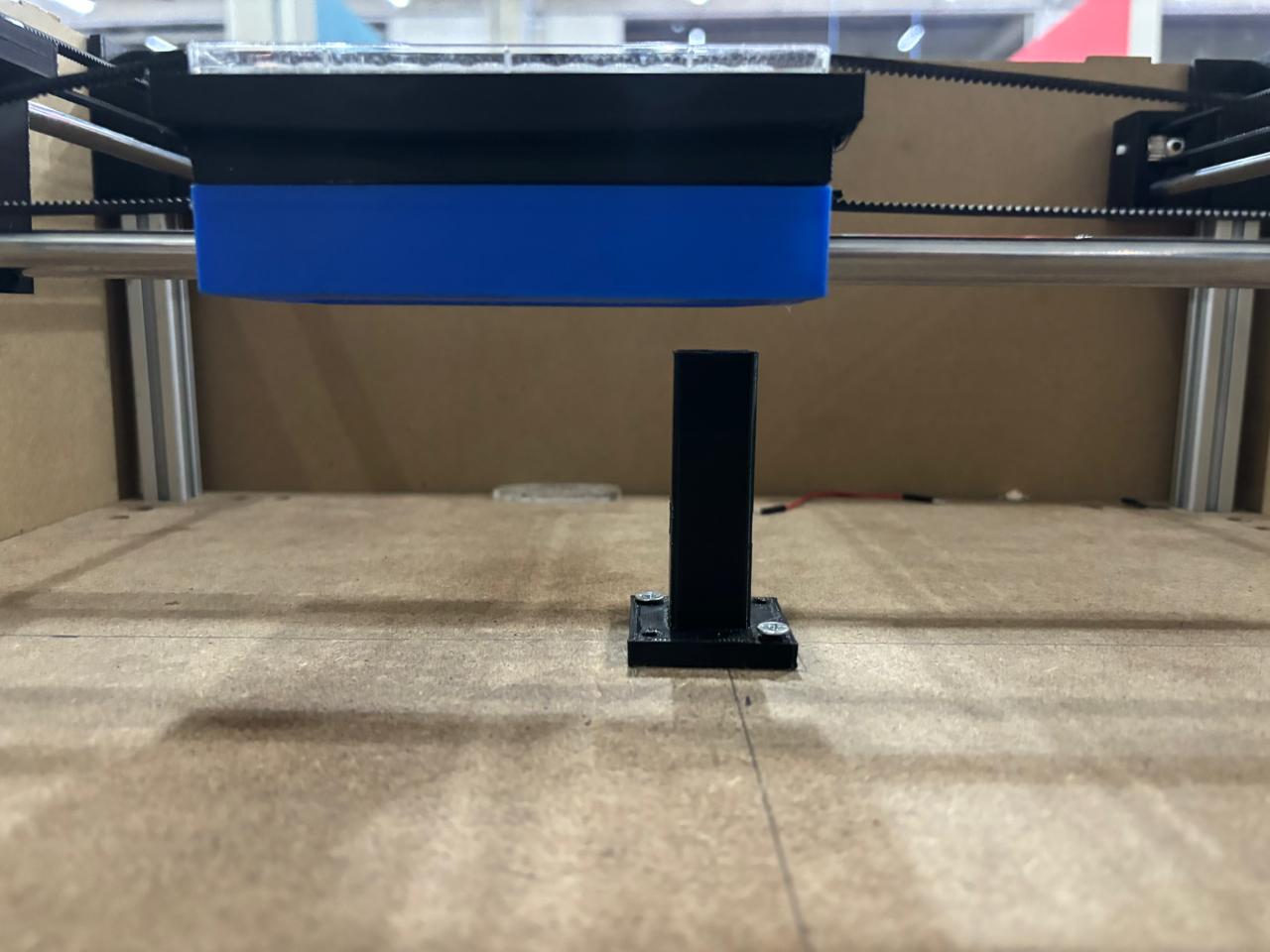
As a physical progress of the project, I designed and 3D printed the black box where I would conduct the LED and sample tests.
Schedule
| Task Number | Topic | Description | Start Date | End Date |
|---|---|---|---|---|
| 1 | Mechanism Design | In this phase, I will focus on designing the mechanical components required for the project. This includes creating a 3D model of the structure that will house and support the system, ensuring functionality and stability. | Week #15 | Week #17 |
| 2 | Electronic Design | This stage involves designing the electronic circuit and selecting the appropriate components, such as sensors, microcontrollers, and LEDs. The goal is to create a functional system capable of collecting and processing data effectively. | Week 18 | Week 19 |
| 3 | Assembly and Simulation | Once the mechanical and electronic designs are complete, I will assemble the physical components. Additionally, simulations will be conducted to test the system’s functionality, ensuring that all parts work together as intended before physical implementation. | Week 20 | Week 22 |
| 4 | Wavelength Evaluation | Here, I will analyze and calibrate the system to ensure it detects and processes light at the specific wavelength required for copper detection. This step is crucial for the system’s accuracy in identifying and quantifying heavy metals. | Week 15 | Week 19 |
| 5 | Sample Preparation | In this phase, I will prepare samples with varying concentrations of copper for testing. These samples will be used to validate the system's ability to accurately measure copper levels and ensure consistent results. | 13 | 22 |
Final project requirements
The CuMeter, What is it?
November 1, 2024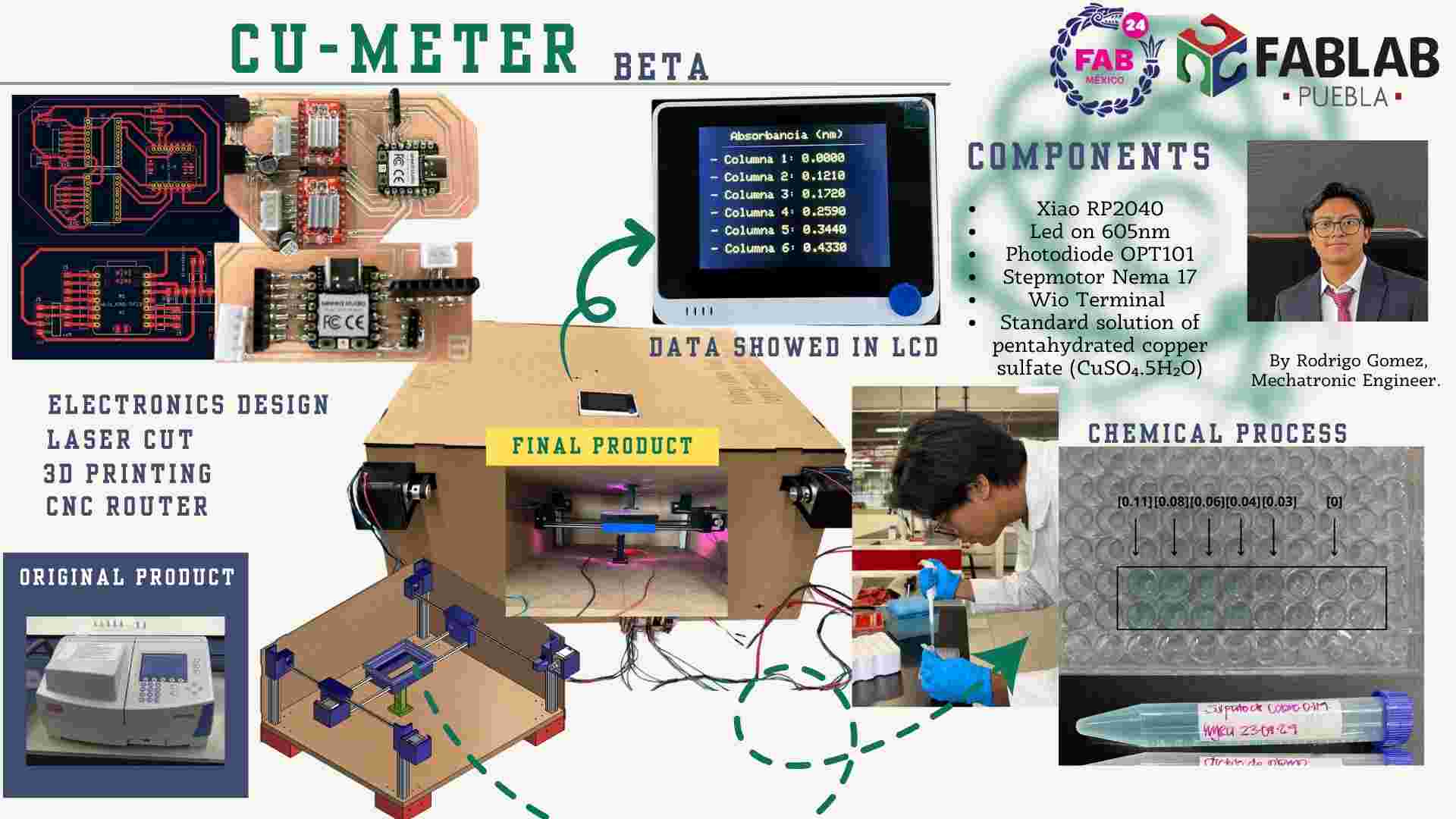
Introduction
The CuMeter was born from an idea during my social service, where I visited different communities in Puebla dedicated to pottery. In Mexico, pottery is glazed with lead oxide, which, when in prolonged contact with food, contaminates it and causes severe health issues, such as reduced IQ in young children. Currently, there are no regulations ensuring the sale of lead-free pottery products. Organizations like Pure Earth work to help artisans transition to lead-free pottery, but this process is often too expensive for pottery-making families.
This project was designed to support the quantitative detection of lead. However, detecting lead posed challenges due to its absorption wavelength. The sensors and LEDs operating within this wavelength range are not easily or economically accessible. As a result, I shifted the project's focus to another heavy metal, which is also present in various pottery products. This metals absorption wavelength falls within a spectrum that is more accessible for the required sensors, allowing the spectrophotometer to function effectively.
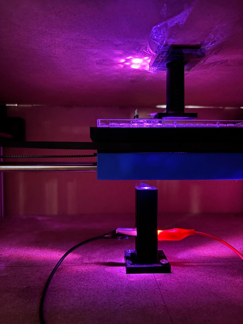
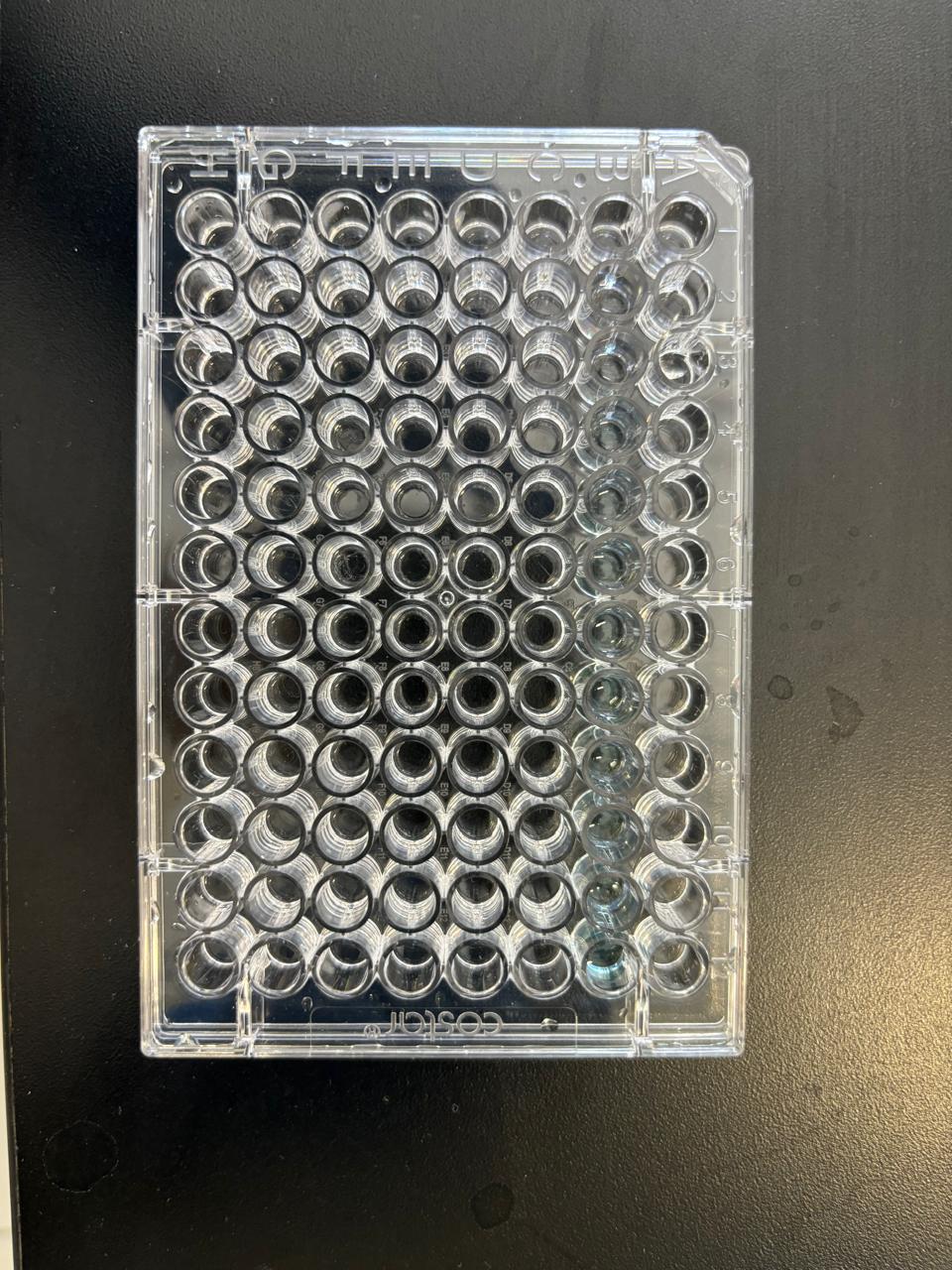
The CuMeter can measure the absorption of a prepared solution to detect the presence or absence of copper. It works by projecting a beam of light through each sample, which is moved by a CNC system to evaluate the necessary samples in the microplate. The OPT101 photodiode then measures the amount of light that passes through the sample, and the program calculates the ratio to finally display the results on an LCD.
Who has done what beforehand?
There are several projects focused on building a spectrophotometer from scratch. In fact, Seed Studio offers a module for conducting tests in the visible spectrum. However, all of these are custom designs and based on personal research. One video I could recommend that showcases another version of a spectrometer is this one.
These devices are quite expensive due to the components required to operate at such low wavelengths. Among the most costly components are:
- Light Source: High-quality lamps, such as xenon or deuterium, which provide stable and long-lasting illumination.
- Monochromator: A device that selects specific wavelengths, essential for the instrument's accuracy.
- Detectors: Sensors like photodiodes or photomultipliers that convert light into electrical signals with high sensitivity.
Leading Brand: Thermo Fisher Scientific
One of the leading brands in the field of spectrophotometers is Thermo Fisher Scientific. This company offers a wide range of UV-Vis spectrophotometers, such as the Evolution series, known for its reliable and versatile hardware as well as its user-friendly software.
What parts and systems were made?
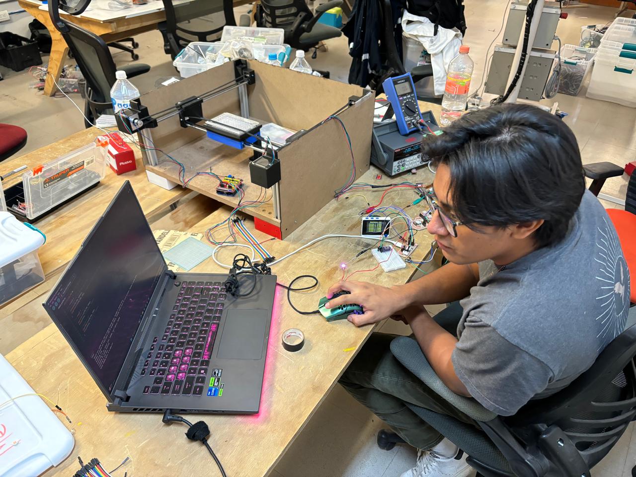
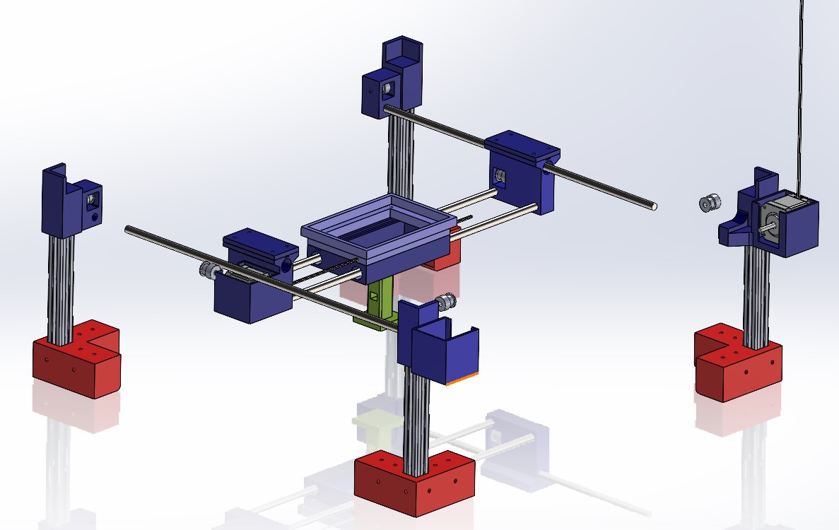
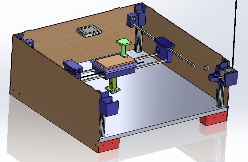
What I designed in this project was the CNC structure in collaboration with my team of the cnc week i asked for permission to use the structure later for my final project, where I applied the principles from Week 10 to my project and used the motor movement system as a reference to build the microplate reader. The microplate reader evaluates one sample in each well of the microplate, requiring both horizontal and vertical movement to analyze samples across all rows of the microplate.
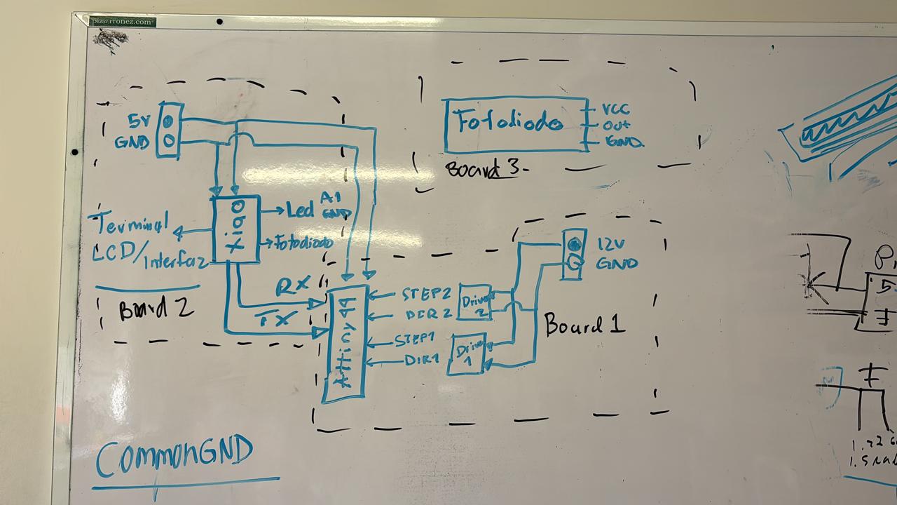
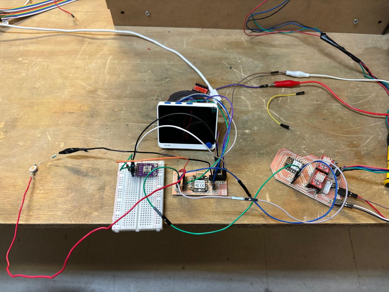
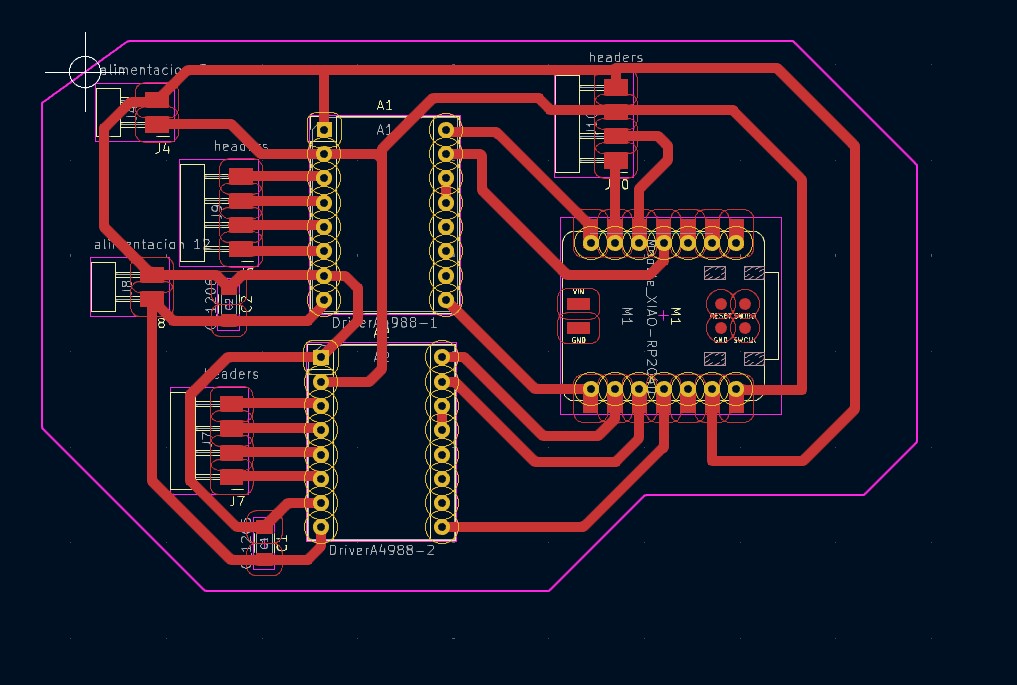
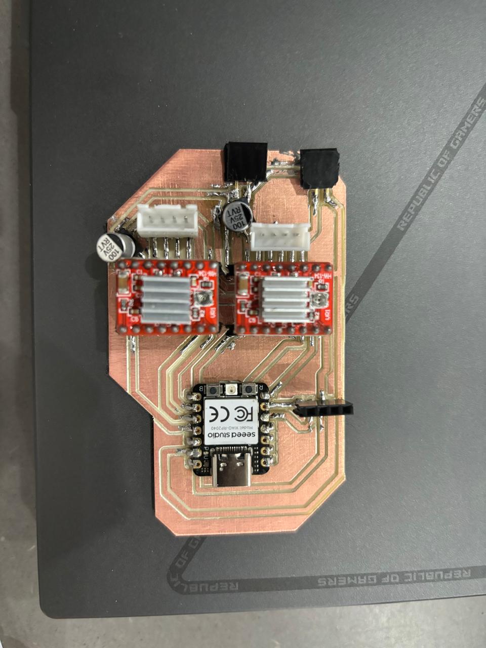
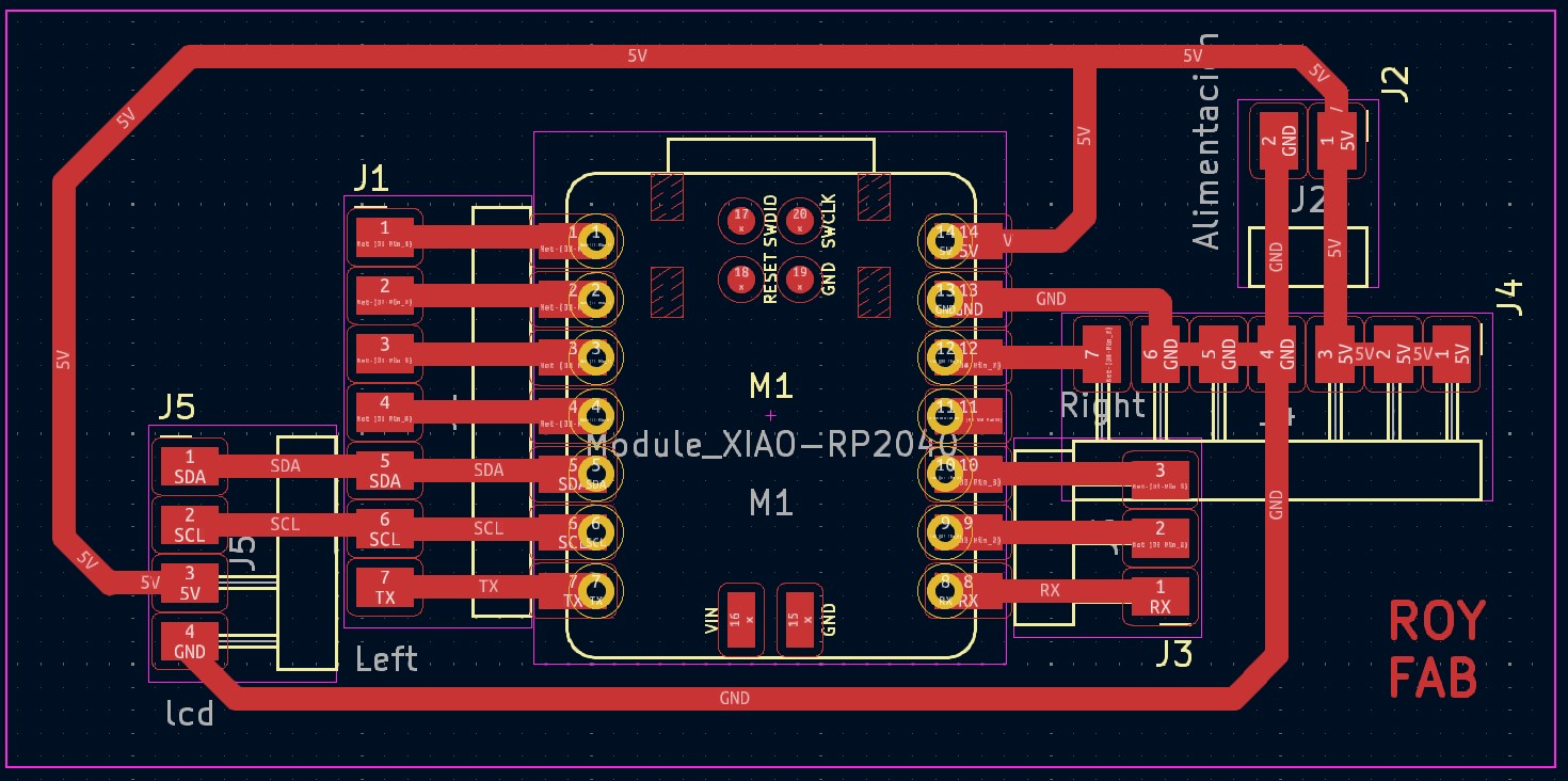
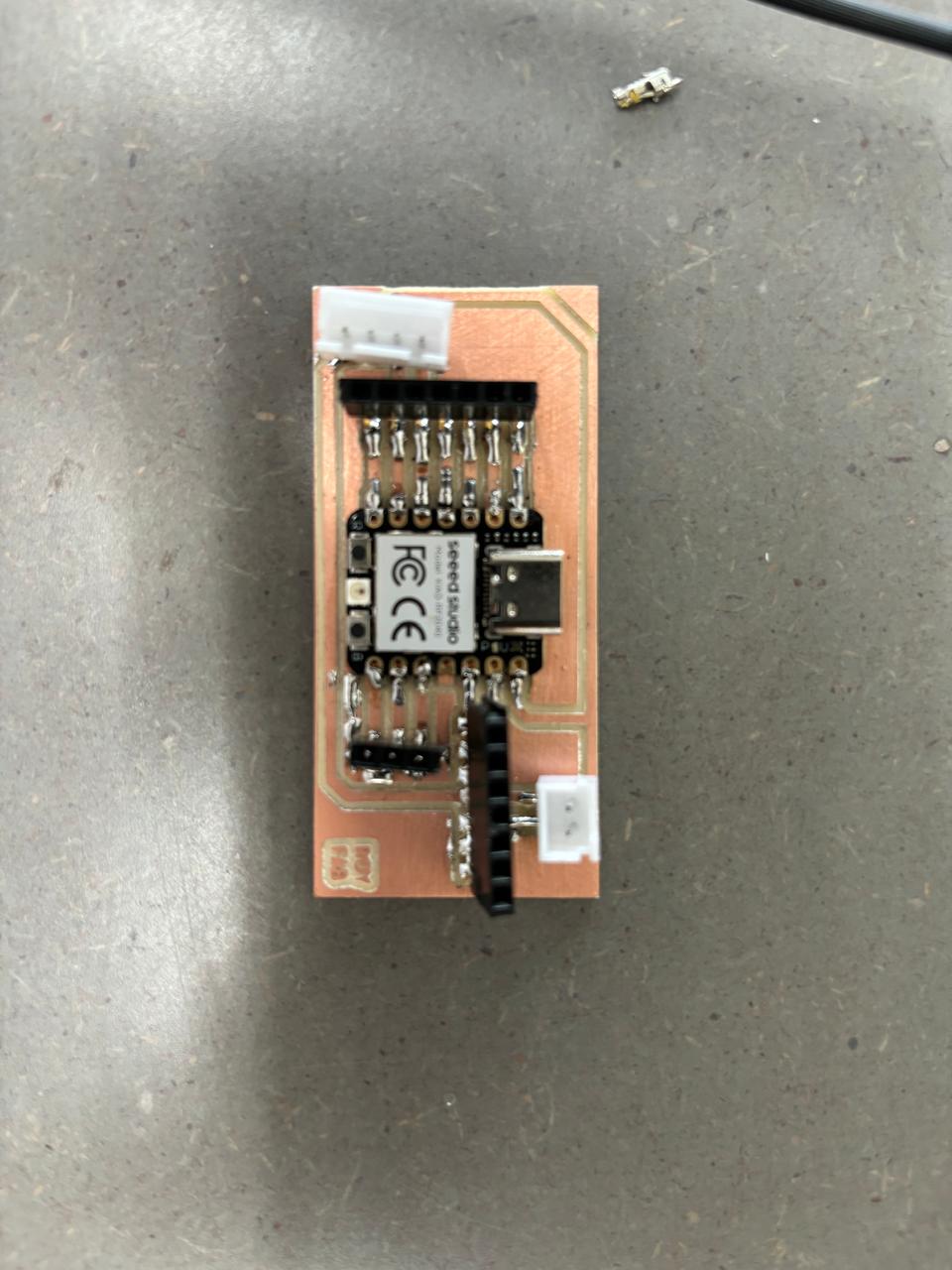
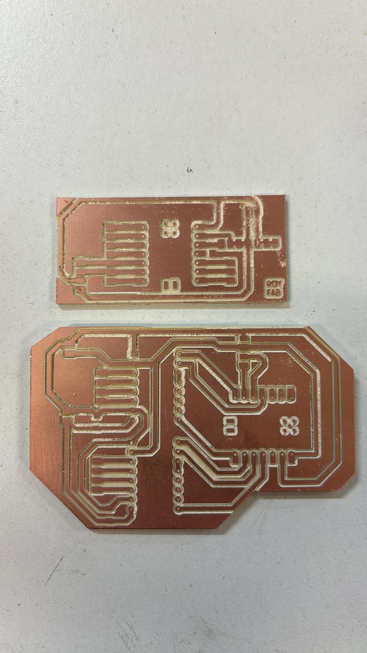
In addition, I developed three PCBs, which integrate the connections for the NEMA17 motors, the LED that generates light, the OPT101 light sensor, and finally, display the results on an LCD. Moreover, I utilized 3D printing, laser cutting, and a router to construct the CNC structure.
System integration
For my system integration I design 3 cases for my pcbs and a LCD Display, i printed on the 3D printer the cases. I made the holes in the corners to used it for assemblying in the MDF 15 mm base.
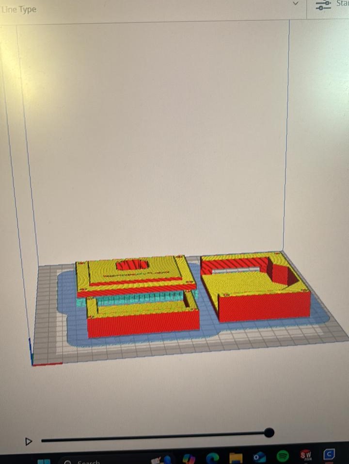
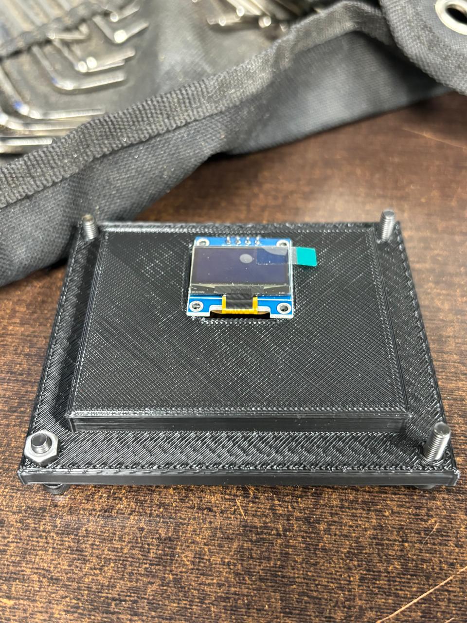
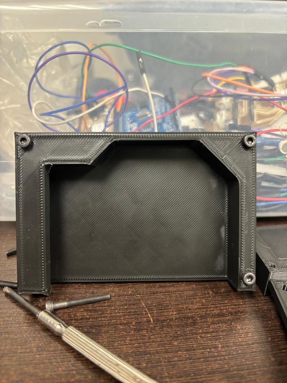
For the installation of the cases, I designed and measured the enclosures that were previously engraved. Earlier, I used one with a terminal, but over the months, it broke down, so I replaced it with an SSD306 LCD Display. Therefore, I developed a case to match the pre-cut MDF measurements. I also printed an LED holder, shown in the middle image, and additionally, the two cases protecting the PCBs are visible in the image on the right.
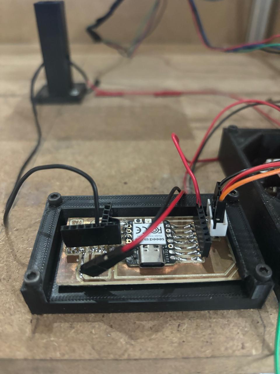
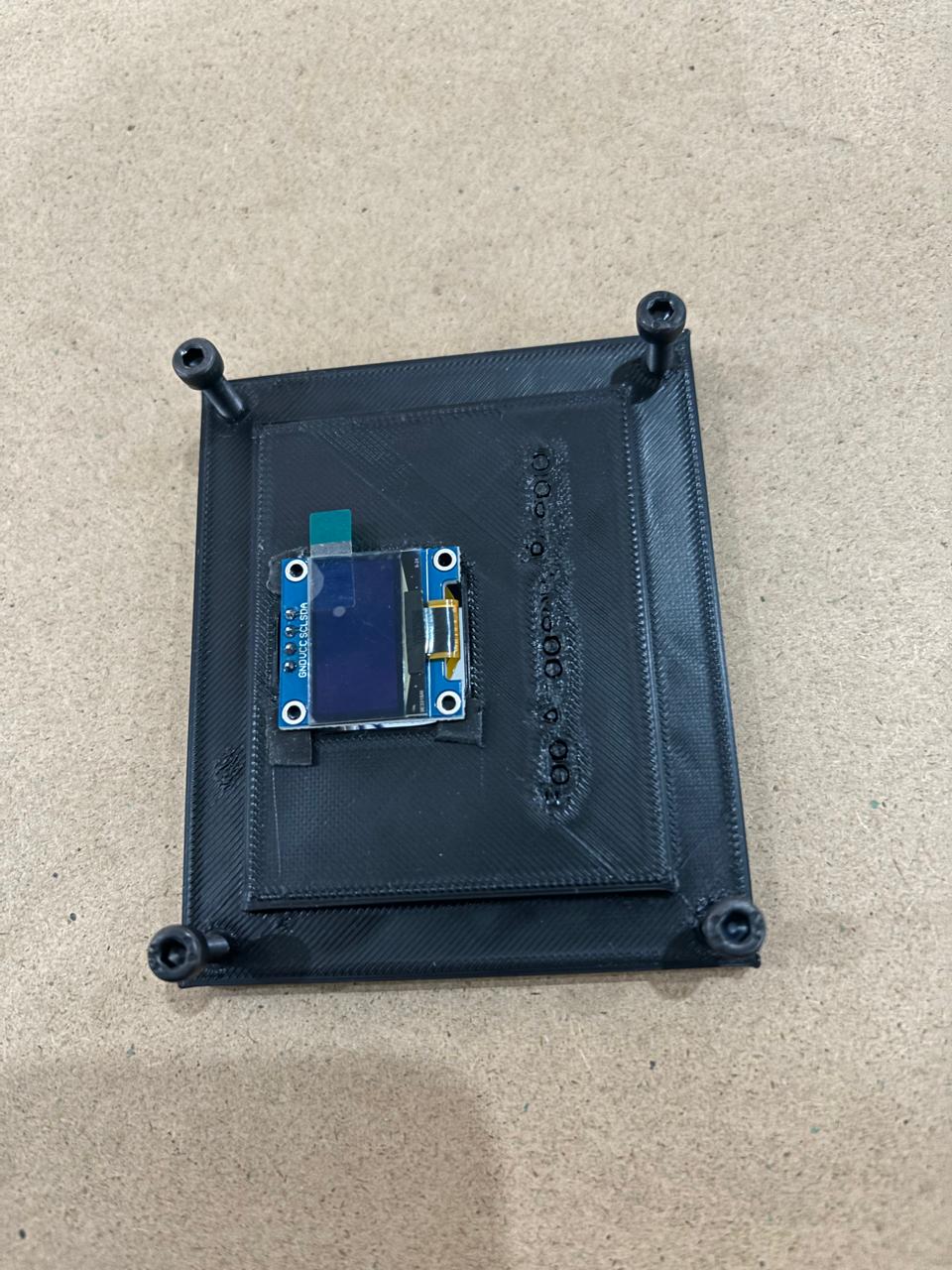
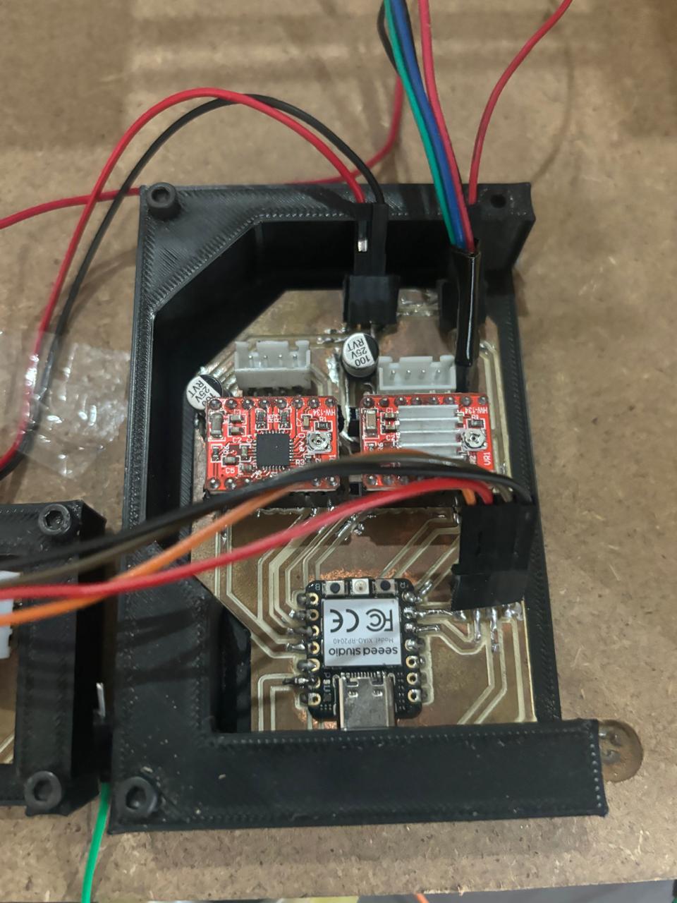
I attached these PCBs using double-sided tape, making them very difficult to remove once adhered. The cases were secured with M3 screws. In the first image, we see four wires—these come from the LCD and are connected with heat shrink tubing. I also applied glue to the heat shrink tubing to secure it to the box, preventing it from hanging and moving around. To minimize strain on the wires and their connection to the LCD, I fastened them to the nearest box.
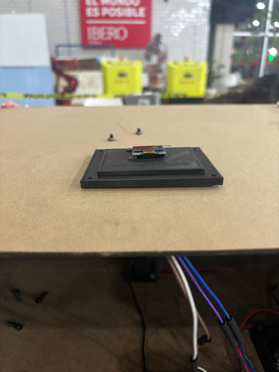
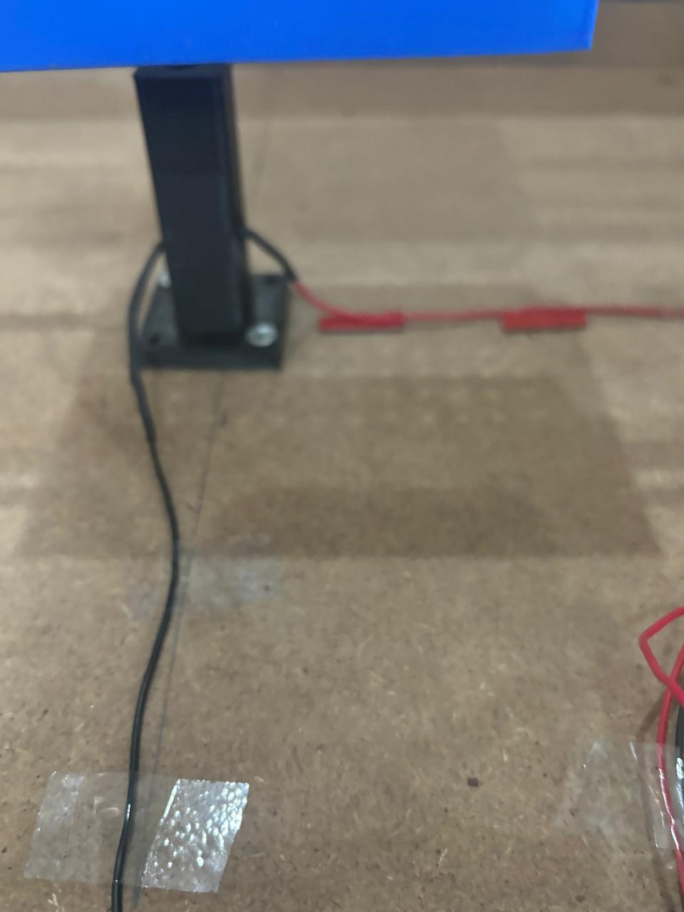
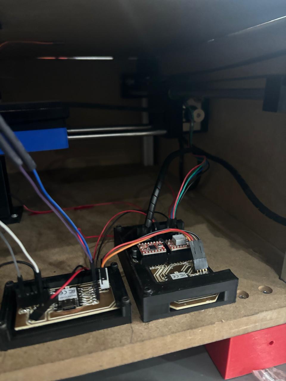
Next is the LED I used for this project. I removed a resistor inside the heat shrink tubing. In the third image, we can see the cable for my NEMA17 motor. I routed this motor cable using a special plastic covering to prevent tangling and to keep it organized.
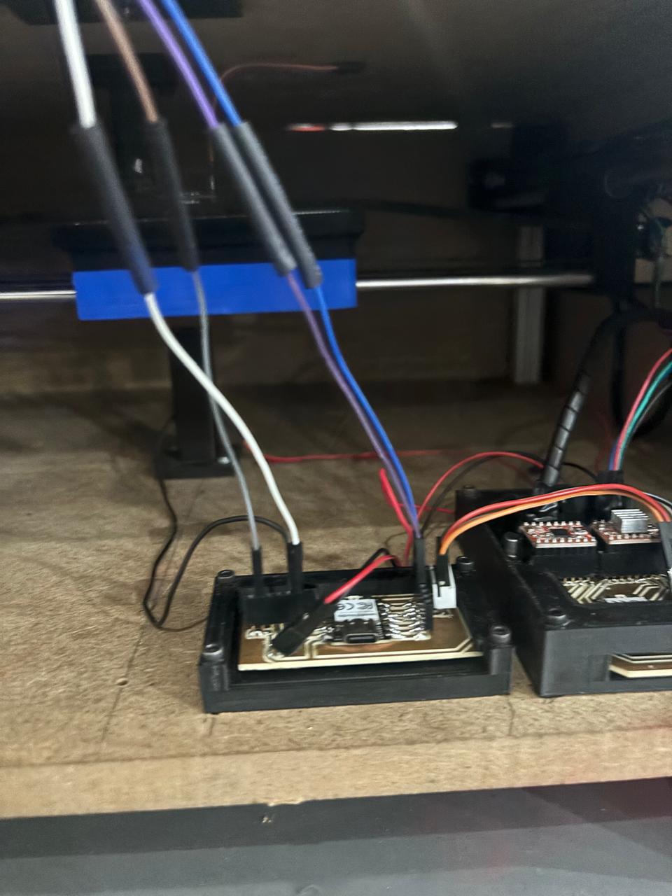
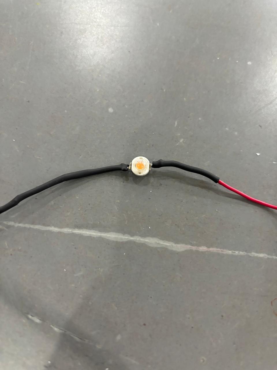
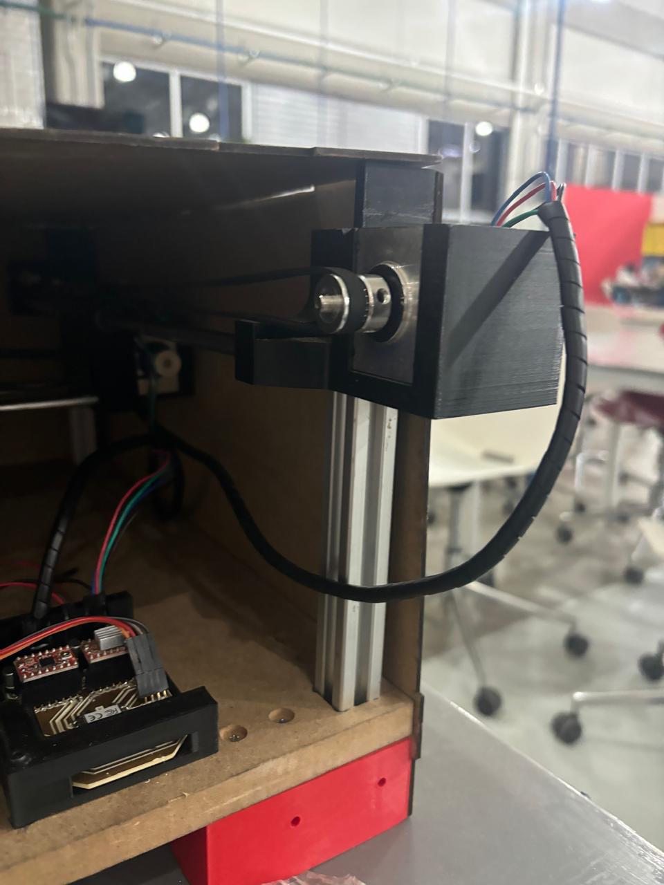
This summarizes the components I used to integrate my project and make it safer and more efficient.
BOM (BILL OF MATERIALS)
| Component | Quantity | Approximate Cost (USD) | Link/Source |
|---|---|---|---|
| XIAO RP2040 | 2 | 6 usd | Seed Studio |
| Male Pin Headers (10-pin rows) | 10 | less than 2 usd | Fab Lab Ibero Puebla |
| LCD OLED | 1 | 4 usd | Unit electronics |
| WIO Terminal | 1 | 30 usd | I had it before the project |
| Soldering tin roll | 1 | 11 usd | Steren |
| Double-sided tape | 1 | 5 usd | Home depot |
| Copper boards for PCB etching | 5 | 12 usd | Steren |
| A4988 Drivers | 3 | 9 usd | Unit electronics |
| 25V, 100uF Capacitors | 2 | Fab Lab Ibero Puebla | |
| 600nm Wavelength LED | 1 | ||
| Multimeter | 1 | 10 usd | Fab Lab Ibero Puebla |
| Soldering station | 1 | 32 usd | mercado libre |
| OPT101 Photodiode | 1 | 22 usd | Mercado libre |
| NEMA Motors | 3 | 13 USD | Unit Electronics |
| Microplate for sample evaluation | 1 | --- | chemistry lab Ibero Puebla. |
| Copper sulfate solution | 1 | - | chemistry lab Ibero Puebla. |
| Red and black wire | 2m | 1usd | Steren |
| Toothed belt and pulley for NEMA 17 motor | 1 kit | 10 usd | Pulley Belt |
Process used
- CAD design for the CuMeter structure
- I used the PCBs design process for the PCBs I developed.
- PCB MILLING
- 3D printing was utilized for joining the profiles and the base.
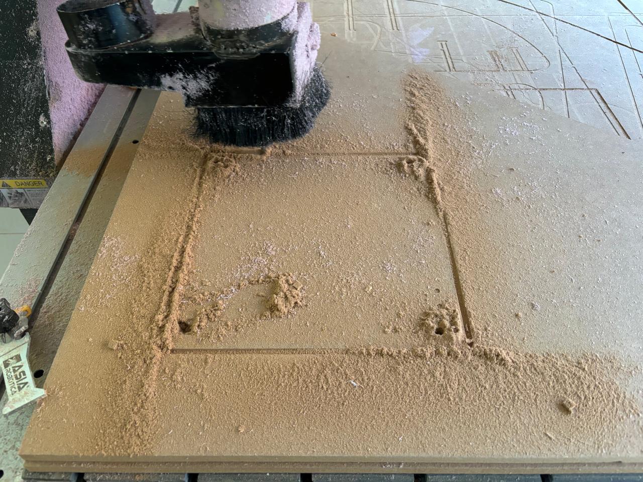
- A CNC router was used for machining.
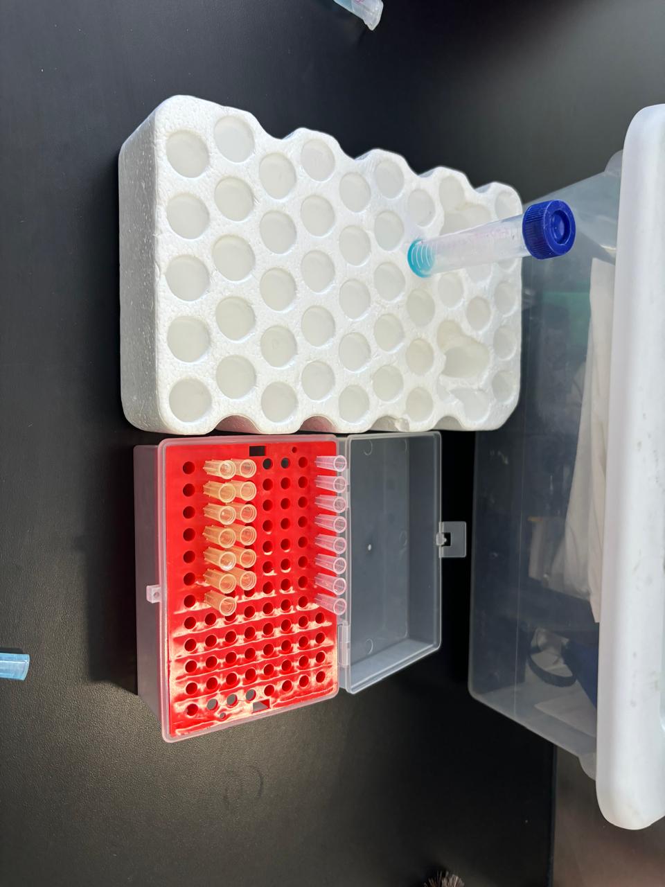
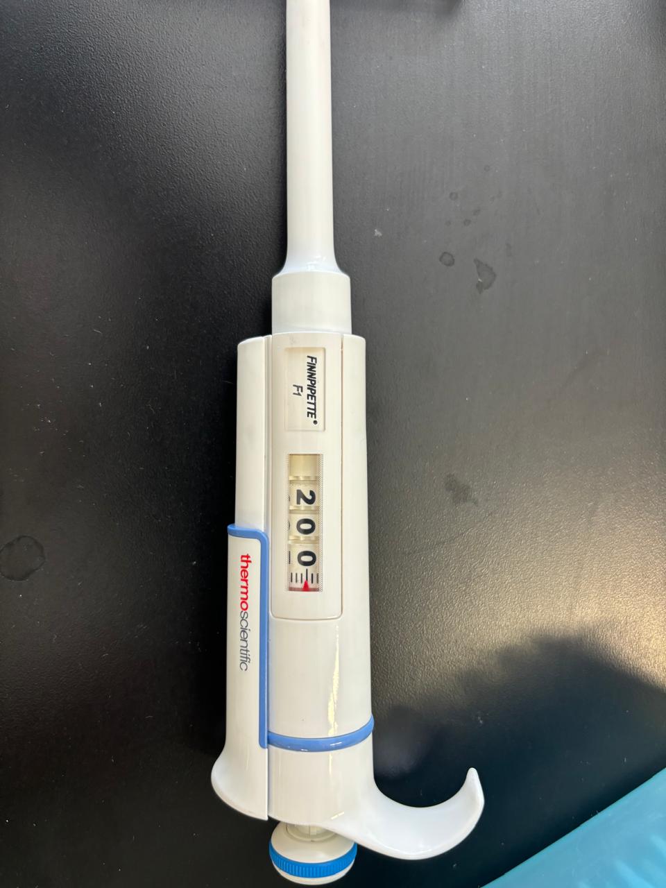
- I also employed a chemical process to prepare the standard solution and reference solution for comparing the results obtained from my project.
Fabrication
What worked? What didn’t?

| CNC Structure | I was unable to obtain an LED that operates at a wavelength of 200 nm. |
| Integration of the boards and communication between them. | Adaptation of the OPT101 light sensor to a custom-designed board. |
| Sampling tests to detect copper using a standard solution. | |
| CNC programming. |
What questions were answered?
Cost and Accessibility:
- How does the cost of this device compare to commercial spectrophotometers?
- Can the components be sourced easily to replicate or scale the project?
Impact and Applications:
- How effectively does the project address the issue of heavy metal contamination in pottery or other materials?
- Could the design be adapted for detecting other metals or substances?
How was it evaluated?
Real-World Testing
- Use real samples from pottery or other materials to detect copper content and assess practical application.
- Gather user feedback on ease of operation and accuracy of results.
Licensing
Creative Commons (CC)
Ideal for making your work widely accessible with minimal restrictions. Variants include:
- CC BY: Allows any use, provided credit is given.
- CC BY-NC: Allows non-commercial use only.
- CC BY-SA: Requires derivative works to be licensed under identical terms.
CuMeter by Rodrigo Gomez Revilla is licensed under Creative Commons Attribution-NonCommercial 4.0 International
