Week 8 Electronics design
Electronic Design Automation (EDA)
Electronics design is the process of creating electronic systems to perform specific functions. It involves choosing the right components, like resistors, capacitors, and microcontrollers, and figuring out how to connect them together.
For this week assigment i would work on designing a PCB.
This list includes essential equipment and tools used in electronic laboratories for testing, measurement, and design purposes:
- Regulated Power Supply - Provides stable and adjustable voltage and current to power electronic circuits.
- Digital Multimeter - Measures electrical values such as voltage, current, and resistance with high accuracy.
- Oscilloscope - Displays voltage signals over time, allowing for the observation of waveform shapes.
- Logic Analyzer - Captures and displays digital signals, helping in debugging digital circuits.
- Mixed Signal Oscilloscope - Combines the functions of an oscilloscope and a logic analyzer, useful for analyzing complex electronic systems.
- Multichannel Oscilloscope - Features multiple channels for simultaneous observation of several signals.
Group Assignment
- Use the test equipment in your lab to observe the operation of a microcontroller circuit board.
- Send a PCB out to a board house.
Individual Assignment
- Use an EDA (Electronic Design Automation) tool to design a development board to interact and communicate with an embedded microcontroller, produce it, and test it.
Extra Credit
- Try another design workflow.
- Design a case for it.
- Simulate its operation.
Group recap
Here i left you our group assigment if you want to see it
- Designing my PCB
- Board
This assigment was a bit chaotic, first i tried to use Eagle, which at the beginning i believed it was a good enviroment to learn how to design your boards, decision i regret. In my tutor class told me, it will be more easy to do it in Ki Cad but i refused to listen at those wiser advices. So i will try to talk a little bit of what i learnt of Eagle and maybe it would help you in something but at the end i explain all my process on Ki Cad which i particularly say is more basic and simple but very efficient, or at least in terms of university stuff.
Also in this week i will start with my first activities of my final project, so these boards would be part in my final project and also complement with the next weeks (input and output devices)
Eagle AutoDesk
First we start with the Schematic, this sheet or document is where you will bring all your components that are going to use, below i left a table with the components i used, basically are just female and male connectors which i will use to conect another components such as my photodiode, my LCD, and the led in the building and function of my final project.
Bill of materials (FIRST BOARD)
| Quantity | Components |
|---|---|
| 1 | XIAO RP2040 |
| 3 | Head Male connectors | \
| 7 | 1K Ohm resistance | \
| 1 | \ |
| 1 | \ |
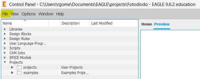
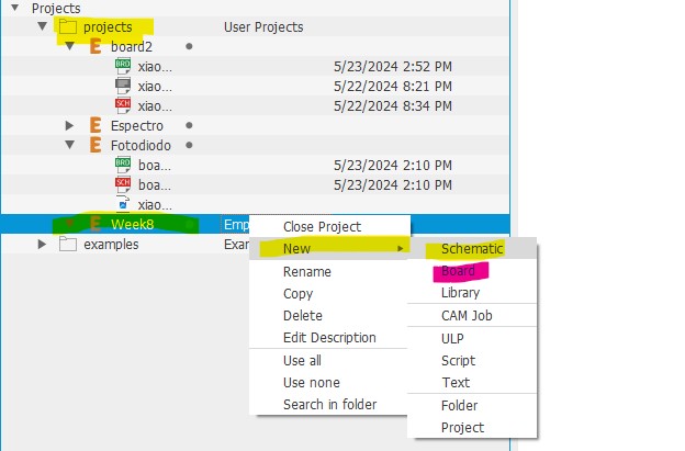
Click on File > New > Project > Click on the project > New Schematic/Board
To add any component you choose to use, click in ADD PART, where you could browse in the eagle library, these aspect of the program is very poor, there are such a few components and in the mayor time i had to import librarys from internet, here is the link where i found a lot of components and their footprints Snap Eda is a nice tool to use if you are using a program like this with not a lot of components but also you can use the link of git hub of the official footprints from fab lab.

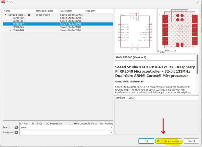
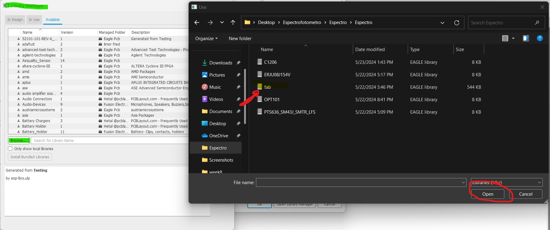
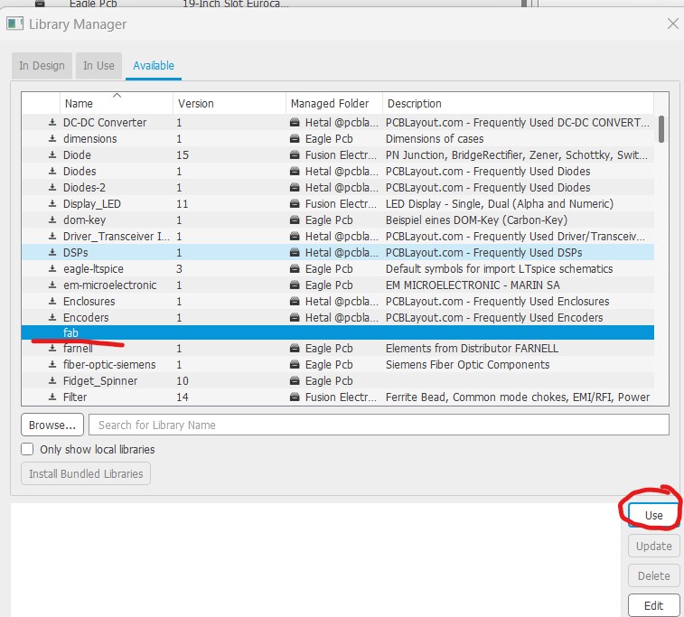
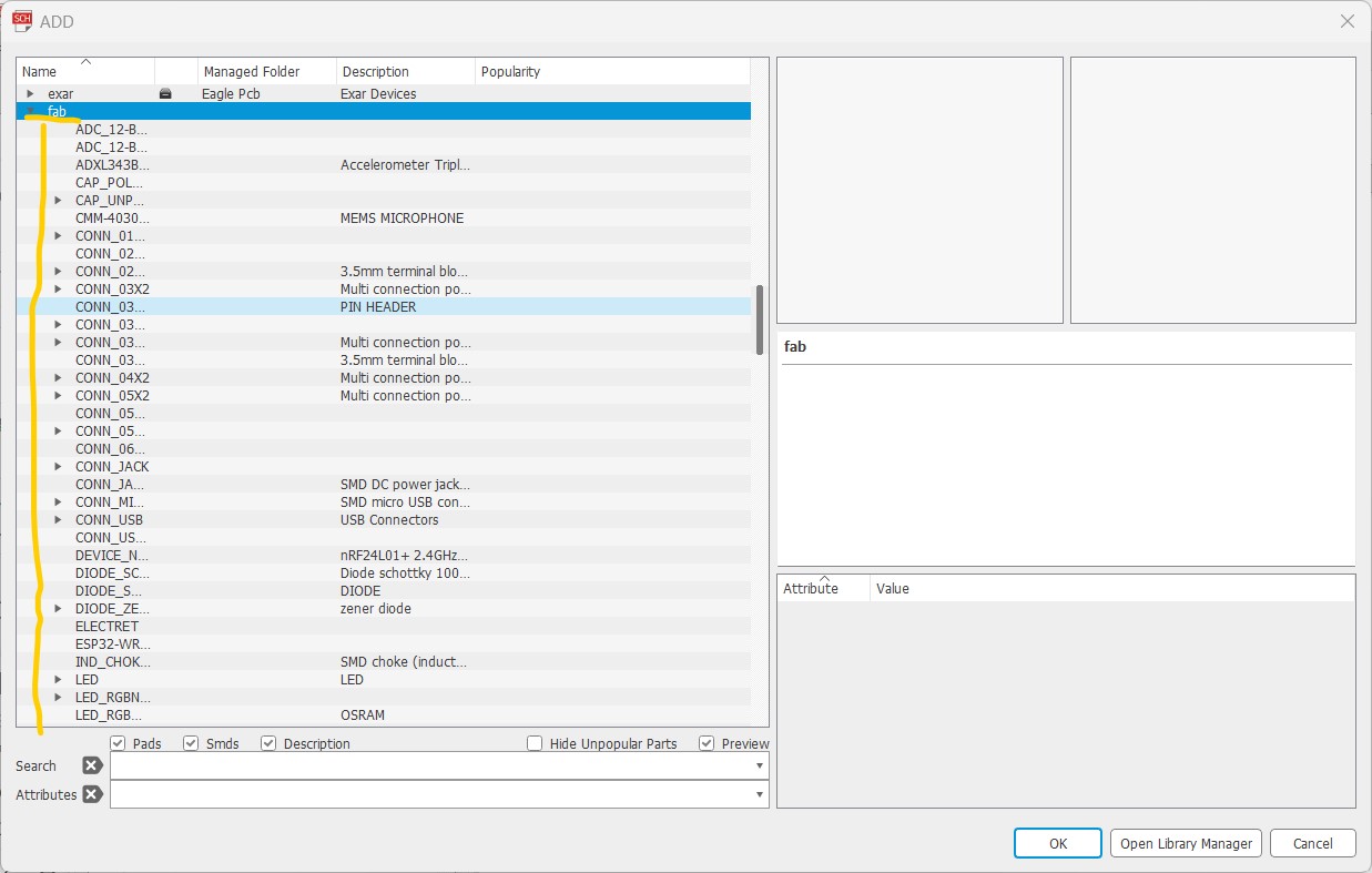
Next, we open the Library Manager and search for the file we downloaded to add the PubLab libraries. I downloaded these in the following folder, then we click on Browse, select the library we want to add, and click Open. After that, we will add the components we need for our board design. All valid and available components from the PubLab folder can be used, as these are the documents and footprints that are valid and accepted by the academy.
ATTINY 24
Now, for the microcontroller I chose, I initially designed a diagram to interact with the ESP32 provided by the university and communicate with the ATINY44. I considered it to be a very powerful microcontroller that takes up very little space. Below, I will share the input and output schematic for the ATINY44.

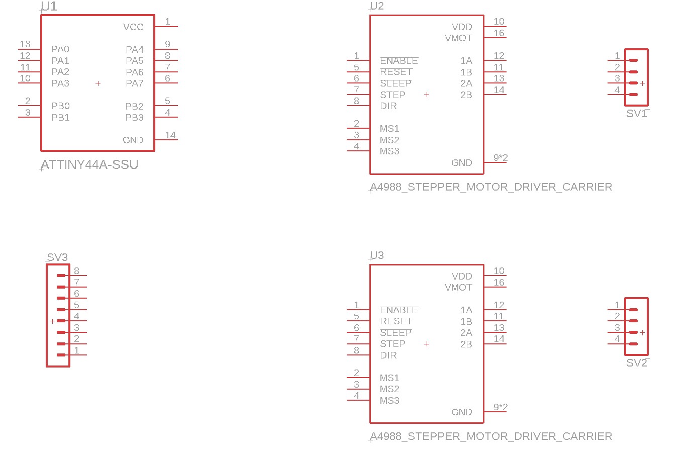
Next, I will import the footprints for the ATINY44 and two A4988 drivers into Eagle. I chose the ATINY44 because it has more inputs and outputs than the ATINY44. For the inputs and outputs I planned to use—two motor drivers plus the inputs and outputs needed for programming the ATINY44 and supplying input and output voltage—I gain 8 extra inputs. Therefore, for me, the ATINY44 was the best choice. These are the components I added.
Next, I will show you some of the tools or shortcuts that can be used for schematic design in Eagle. The first one is the rotate option. This rotate function works with the "R" key and allows you to position any component in any orientation, whether at 90º or 180º.
Headers, rotate

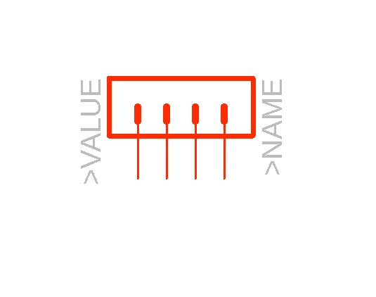
NET
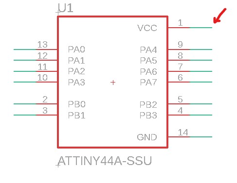
The next tool is "net." The net tool is located on the far right and is very useful for connecting one component to another, such as connecting the ground of the ATINY to the ATINY44 or to the ground of the driver. Next, I'll introduce the "Name" option.
Name
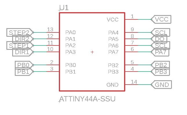
The Name tool helps avoid connecting components with net lines, which can sometimes make the schematic harder to read. By simply naming the connections we want to link with the same name, we ensure they are properly connected.
ERC
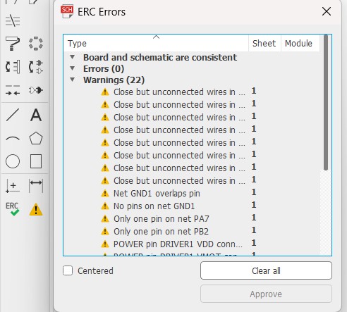
The ERC (Electrical Rule Check) option works by identifying errors in your schematic, helping you see if nets or names are correctly connected.
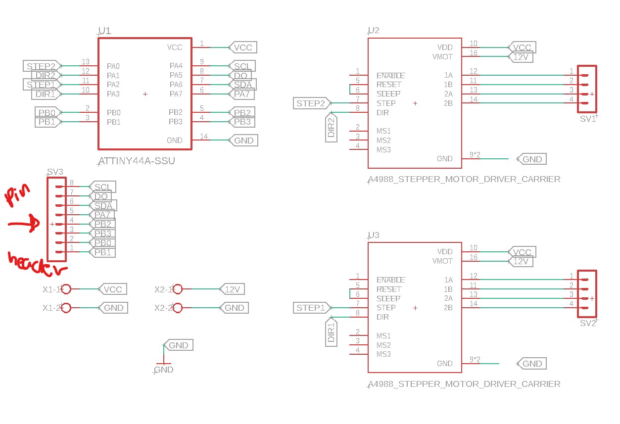
Schematic
Finally, here is how my schematic looks in Eagle—this is the first version where I completed the connections between the ATINY, the two drivers, the input and output voltages, and a ground connection.
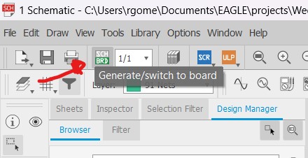
Create board
Now, to arrange our components on the PCB and simulate how it might look in Eagle, we will switch to the "Create Board" option.
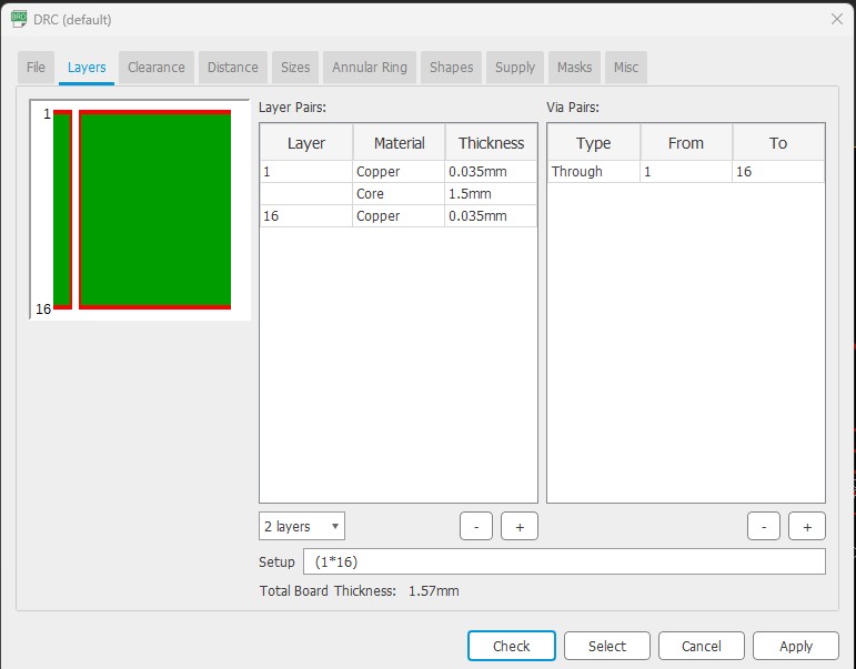
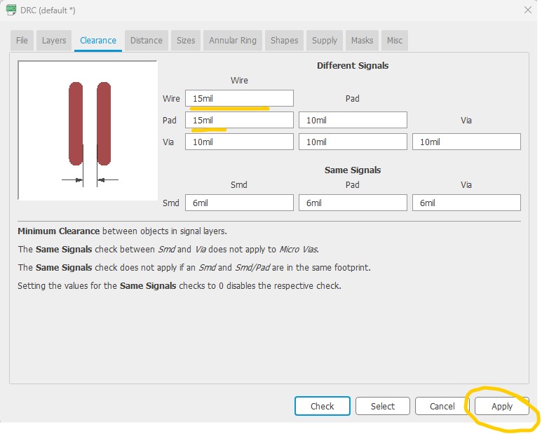
Rules of design
Here, we will set up the design rules as shown below.
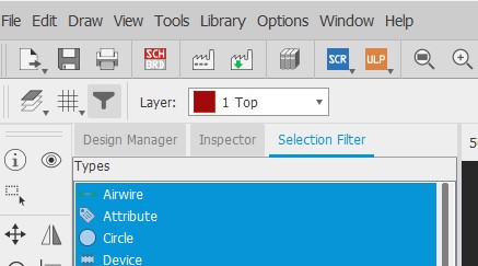
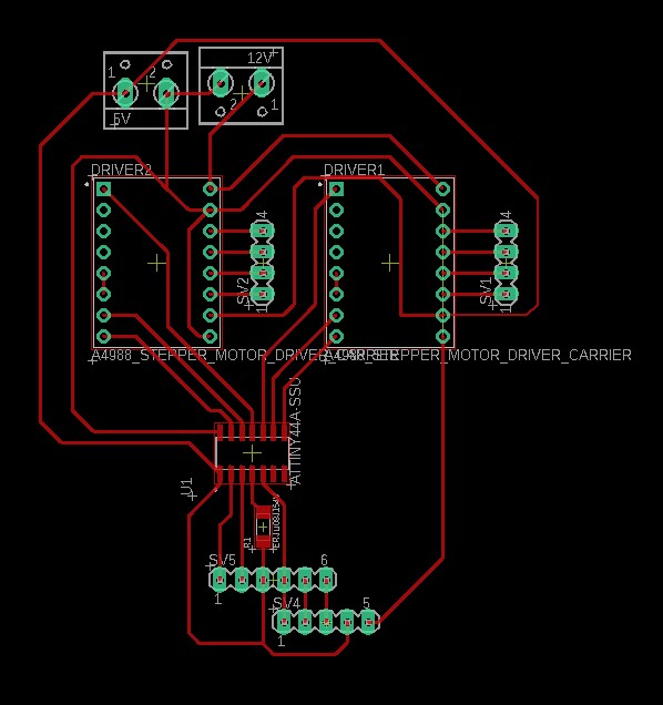
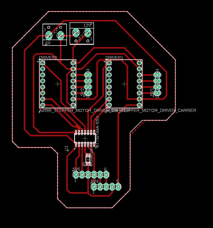
Make sure you are working on Layer 1, which is the red layer called "Top." In this way, I arranged my board so that all connections are properly linked, leaving no yellow lines unconnected.
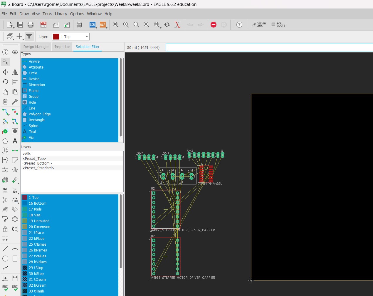
Once this is done, the board will appear in the following way, with components connected by yellow lines that simulate the connection between pads or the nets in the schematic. At this point, we will need to experiment with positioning the components efficiently to avoid overlapping connections, as not all connections can intersect.
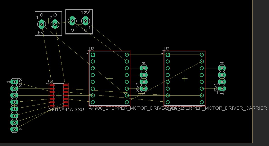
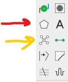
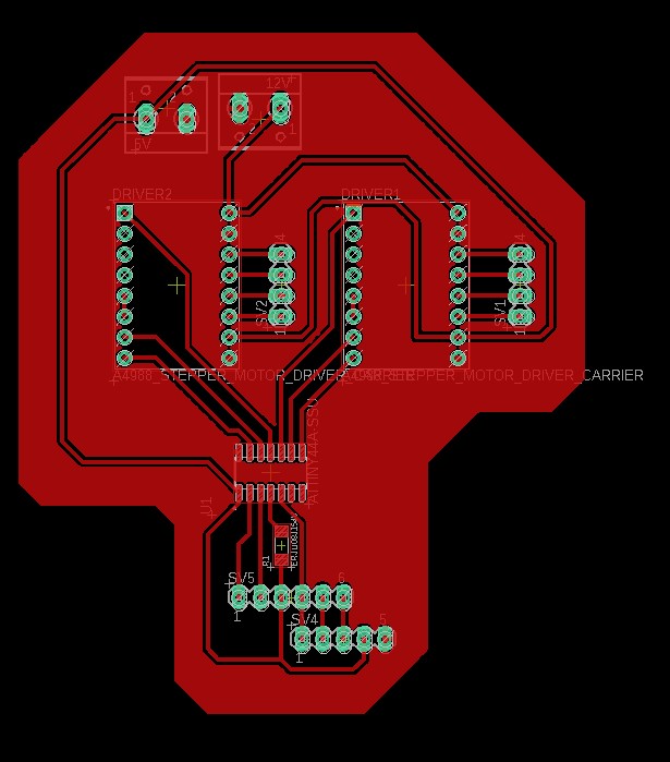
Next, on the right-hand tool panel, you will find these two options. The first option allows you to draw a polygon, ensuring that the area you designate is grounded. This will appear as shown below. All the red areas will be connected to ground, establishing a connection between all the components on our schematic and PCB, thus reducing noise on the board.
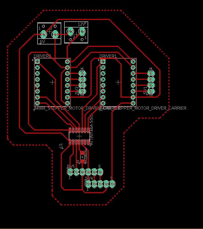
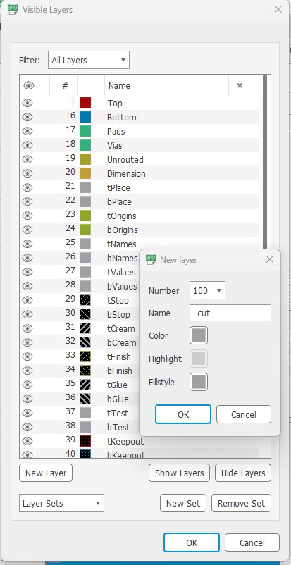
Now, we will create a new layer, which we will name "Cut." On this layer, we will draw the outline of the board we want to cut. This outline ensures that, when we generate the G-code, only the edges will be cut. This edge will function as we have done in previous weeks.
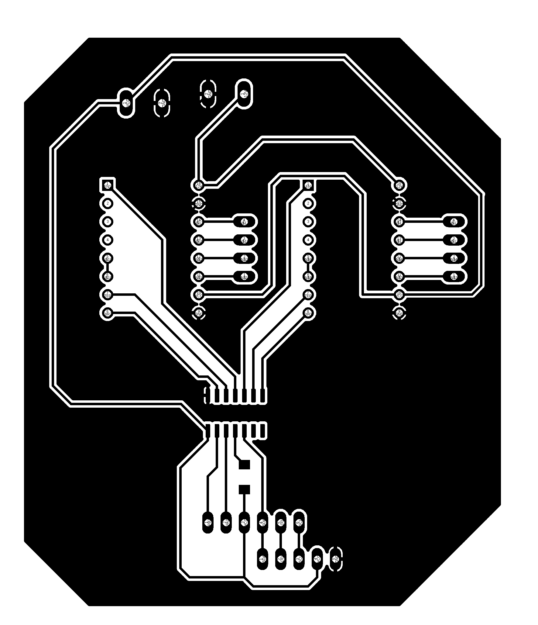
Final monochromatic board to use on MODS CE
KiCad
i decided to use Kicad, because is a open source program, if you want to download it click here
File > New project > save your new project > click right on the file with the _sch ending.
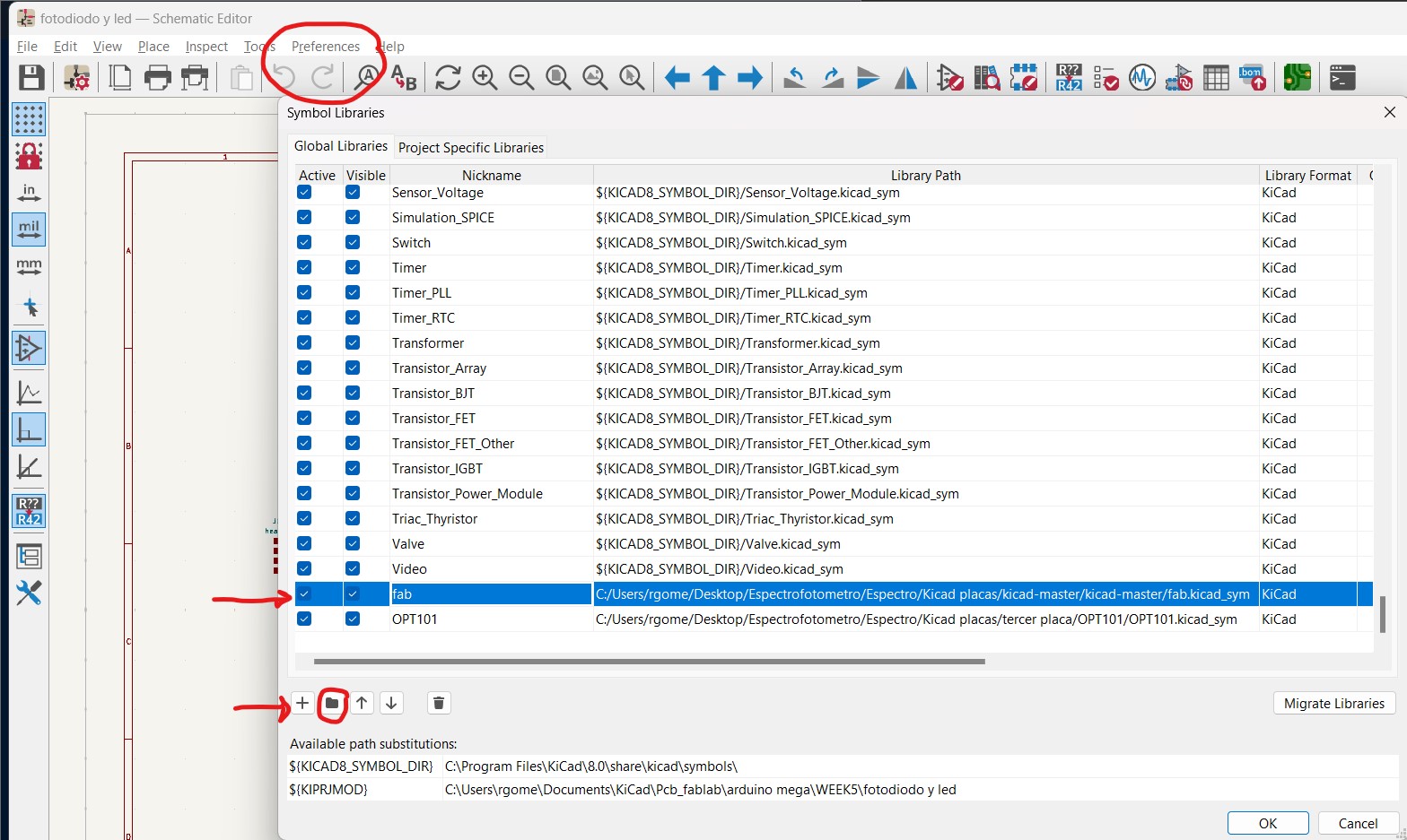
Click on the Preference menu to add a new symbol library. This symbol library serves the same purpose as the library we added in Eagle, since Fabacademy provided us with certain components and footprints that can be used. Below, we will see the components we plan to use.
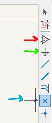
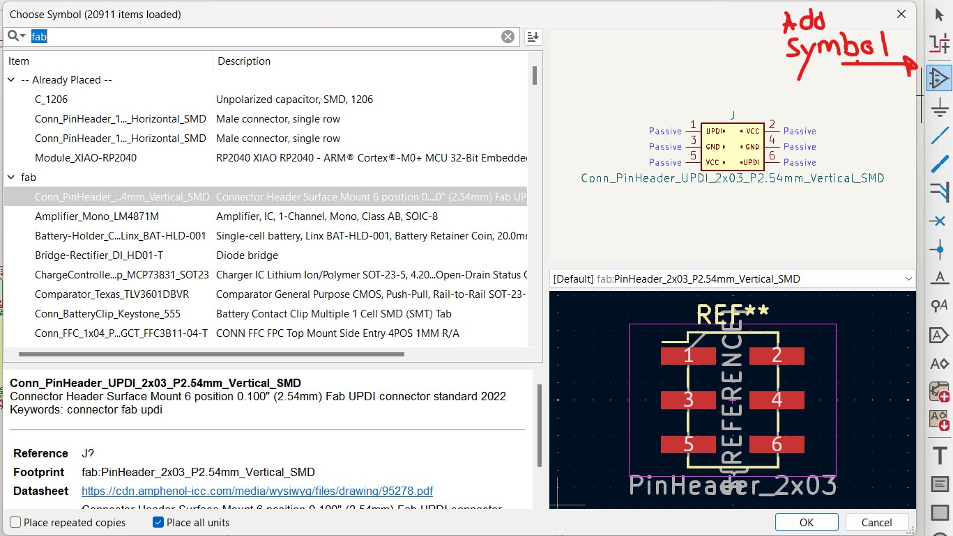
The tool marked with the red arrow is for adding a component. The green arrow indicates the tool for adding power or ground symbols. The blue arrow shows the tool to remove unused connections from our components, such as pins, Arduino connections, or XIAO connections.
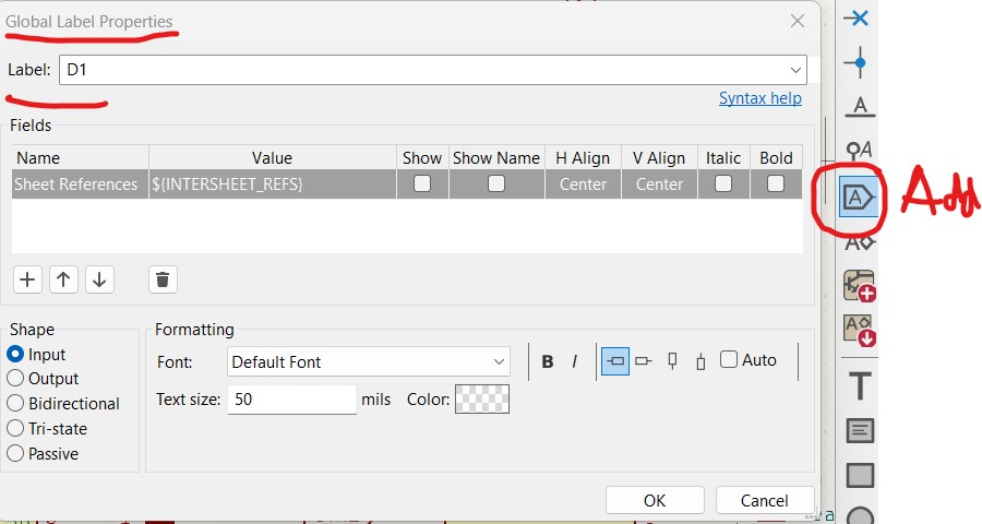
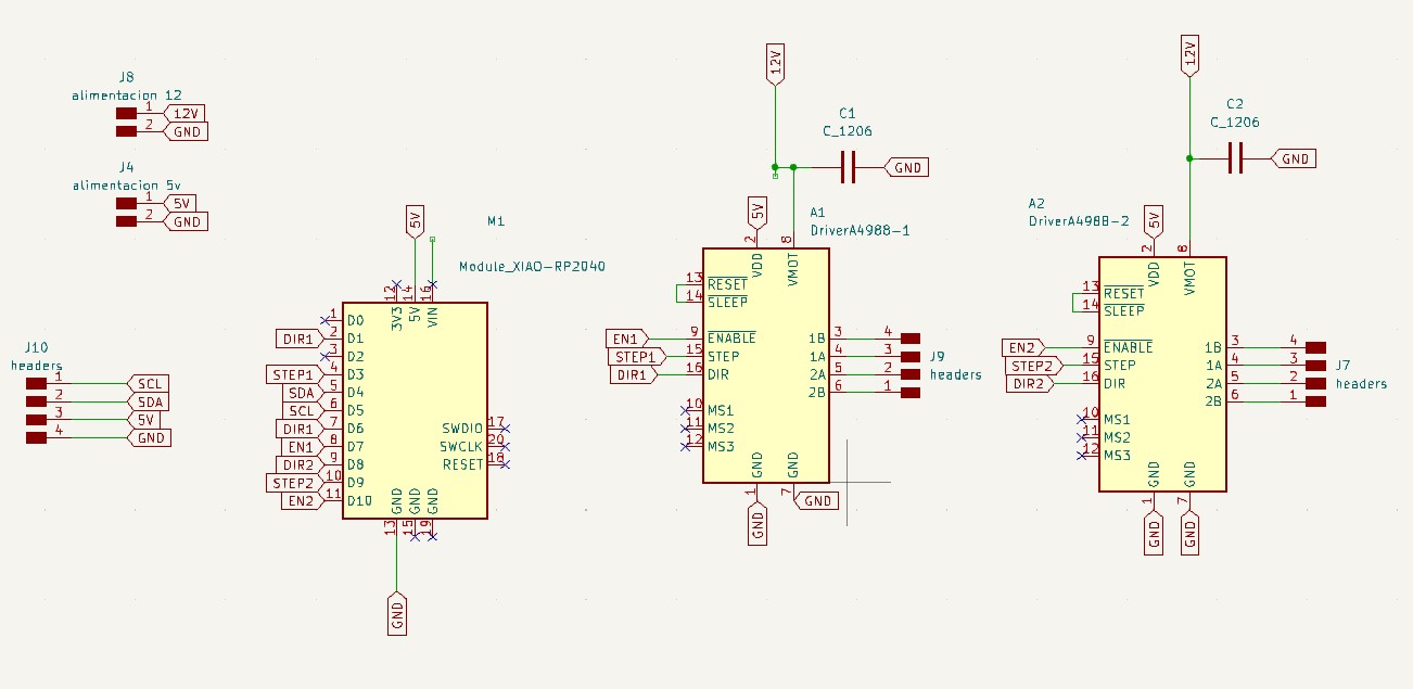
Here, I will once again use a very important tool that I find extremely convenient: adding a label. This label helps me organize all the connections between my XIAO and the drivers I will use for my NEMA motors more neatly. I selected the first component to add: the XIAO RP2040 module.
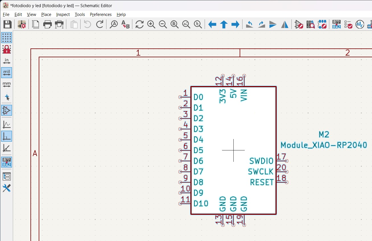
Finally, I obtained this image, which shows the schematic of my first self-designed board.
click on "Update PCB from Schematic," where I can check for errors and convert the schematic into a PCB layout. Below, I’ll provide an example of how the transition from schematic to PCB looks, showing how the components must be connected using blue lines.

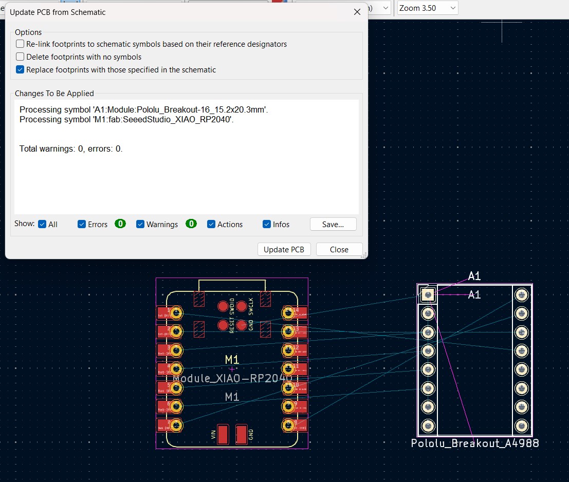
These blue lines highlight the necessary connections in yellow, making it clear which connections need to be made. For me, this was a very intuitive program because there’s no way to accidentally connect to the wrong pin—it’s impossible.
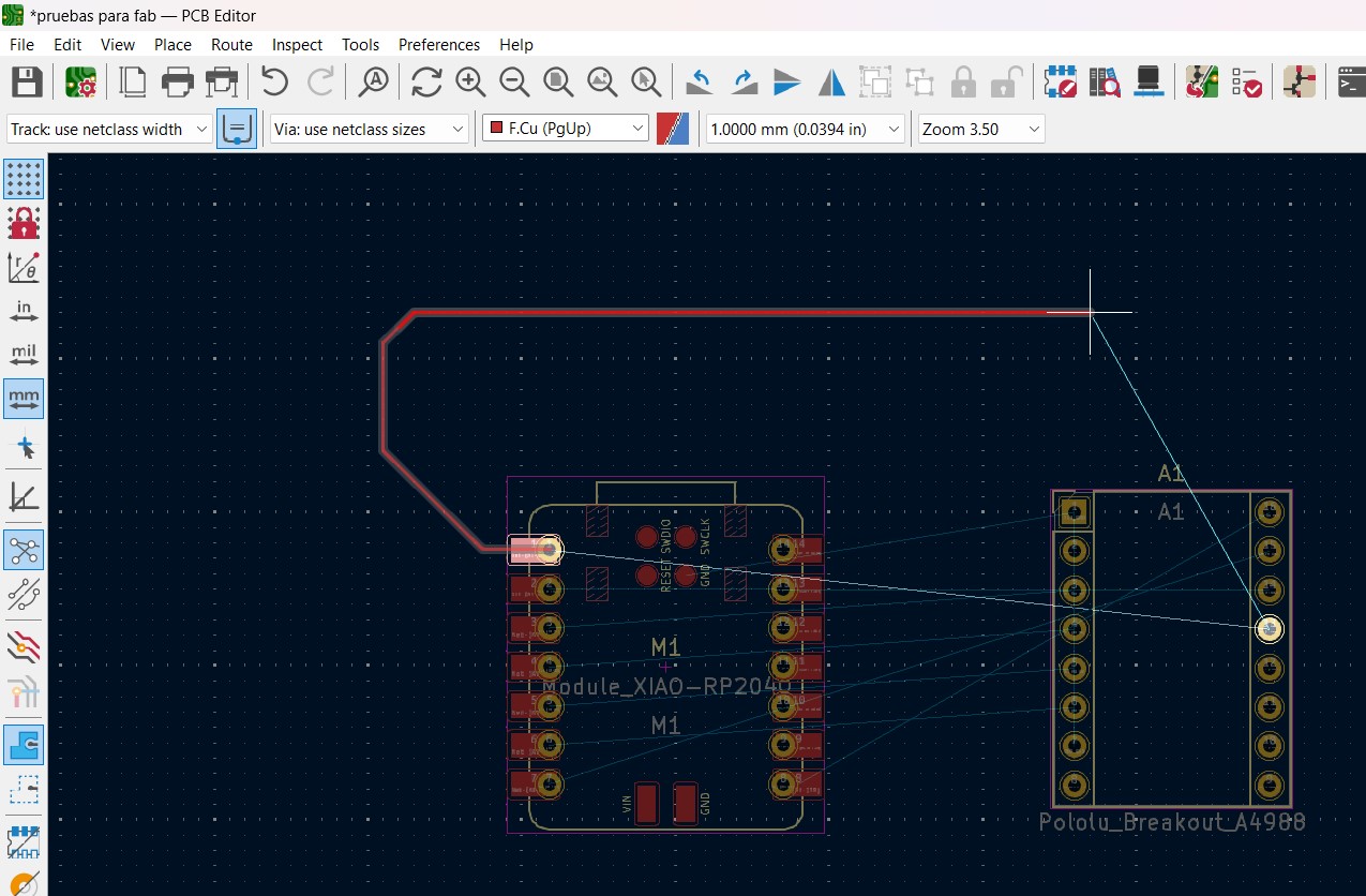
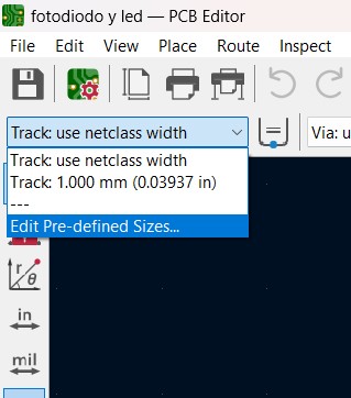
Also, let’s not forget to select the PCB rules and set the spacing between each pad. Below, I’ll show you the Board Setup that I used.
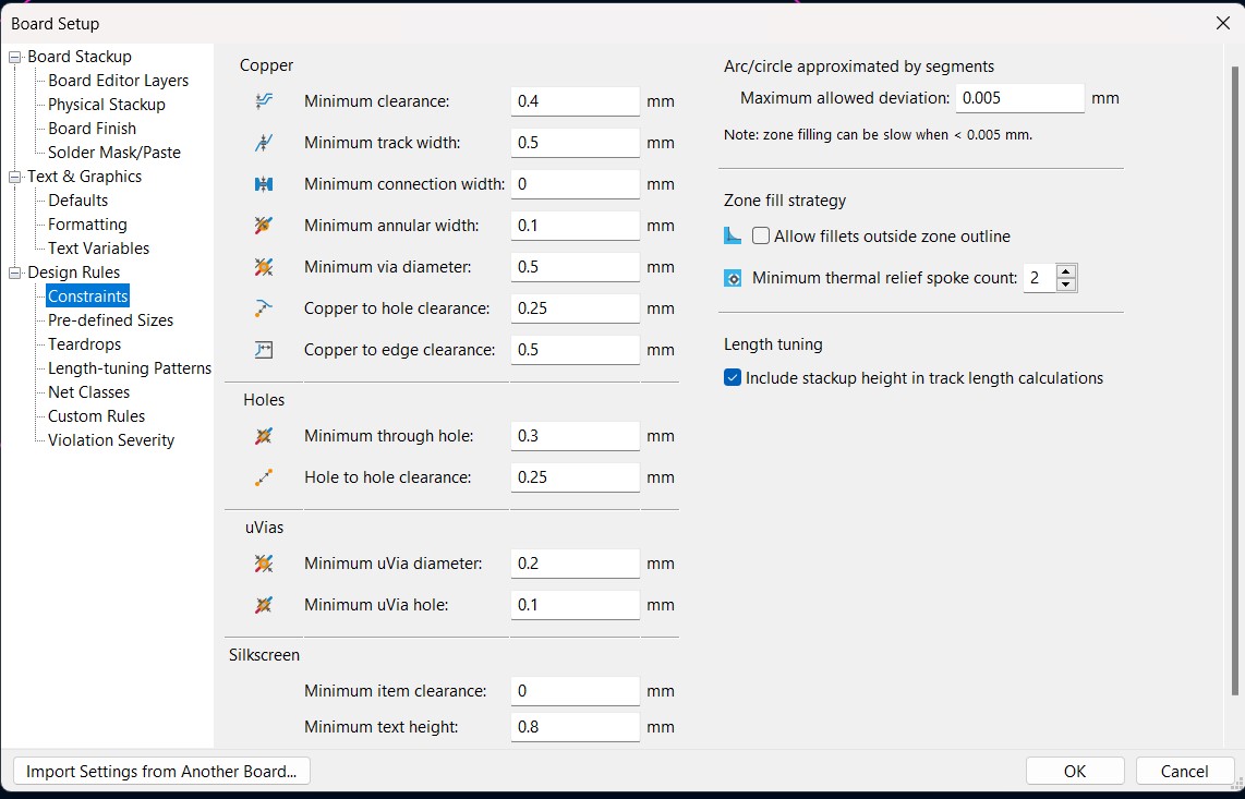
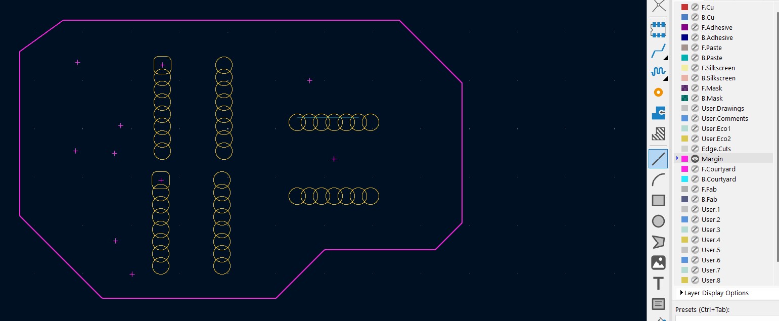
Finally, I’ll mark the outline I want to cut by drawing a line in the margin layer. This is the final image of my PCB, with all components connected and the edge marked for cutting
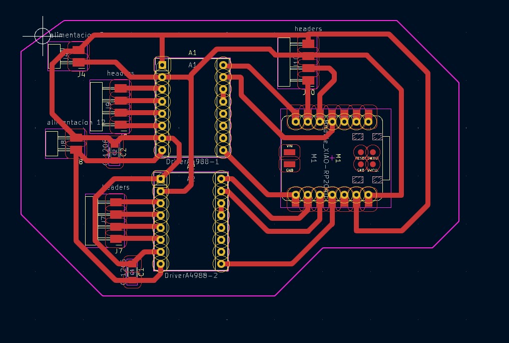
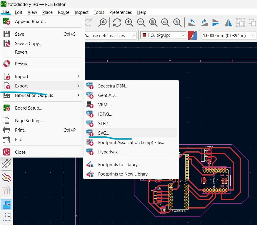
How to export the image as SVG FILE :
I trully recommend this format to cut with the roland.
Conclusion & thoughts
Personally, I chose to use a different program to design my PCB. Initially, I tried to do my first test with Autodesk Eagle. At first, the program seemed very easy to use. However, I started encountering many problems when I tried to export the files to generate the G-code. This was because, firstly, it was not the program taught in the university or in the FabAcademy. I had already learned to use this program in other classes, so it was easier for me to return to what I knew and design my boards in this program.
However, there was an issue with the final image where the connection points for the components were shown. These were supposed to be holes or simple connection pads, but I couldn’t figure out how to remove the connection numbers. This turned out to be a problem. Additionally, I couldn’t find a way to adjust the pad thickness. After some thought, I decided to try another program, and I was recommended KiCad. I found KiCad very easy to learn, though starting from scratch meant dedicating more time to mastering it.
Comparing the two programs, I would say that KiCad is slightly more user-friendly and self-taught for students, while Eagle might be more suited for professionals or those more experienced in PCB design. Eagle offers more tools and a broader working environment, making it a more complete and powerful program. However, for my current needs, KiCad was more convenient due to its ease of use, the availability of tutorials, and the accessibility of libraries and footprints.
How
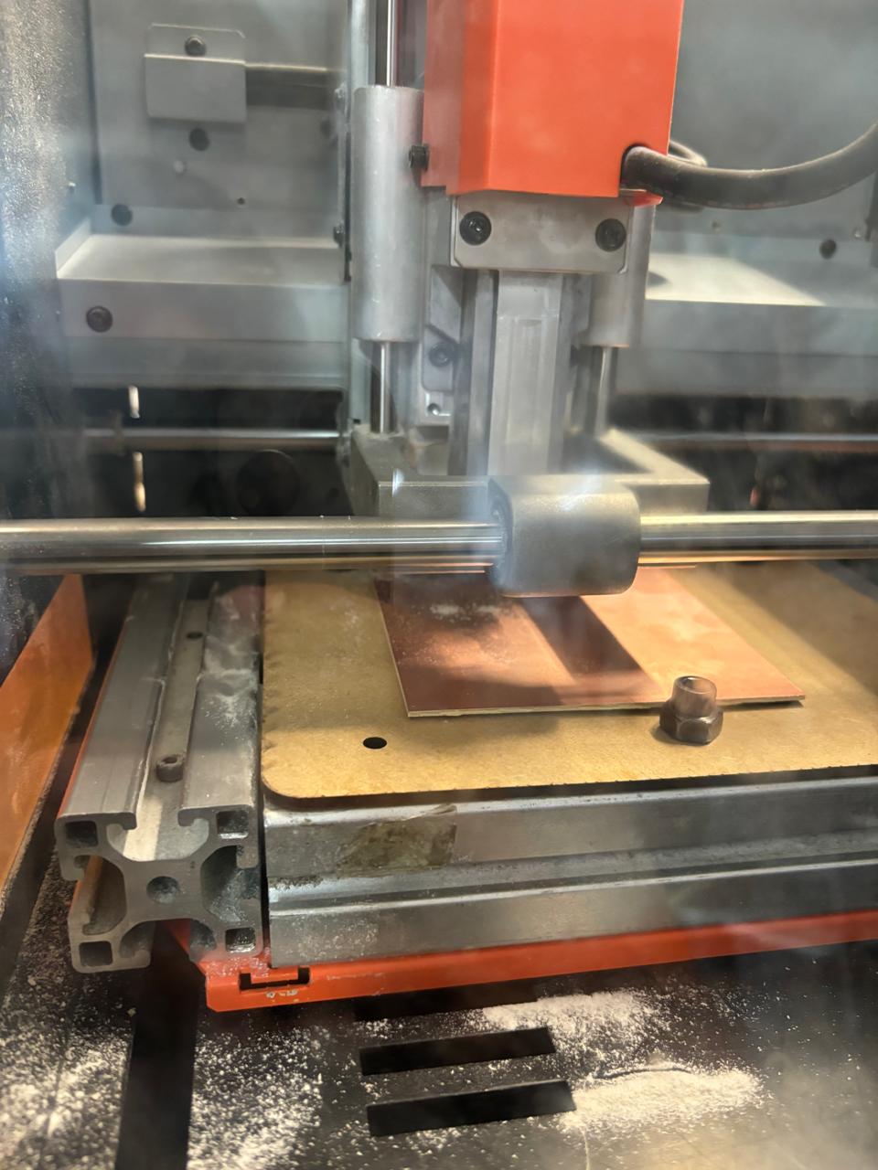
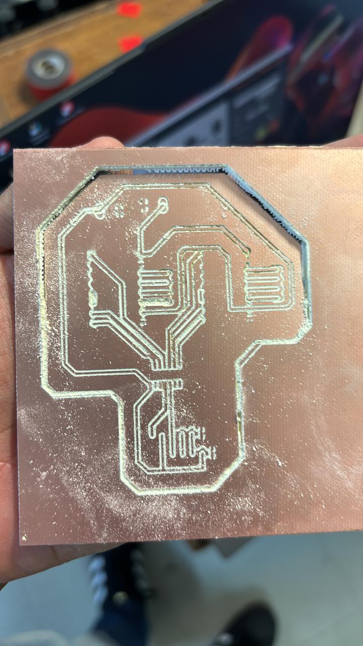
Next, I will show you a bit of the process I followed to manufacture my PCB. However, this process was previously documented and detailed in one of the earlier weeks, so I will provide a more general overview. I made over six attempts throughout the development of this week. Here, I will show you some of the attempts I made.
This one is the one i made in eagle
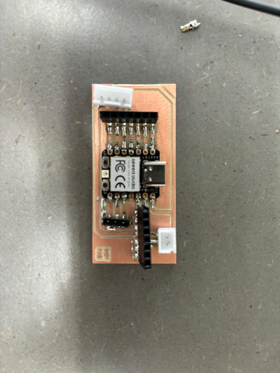
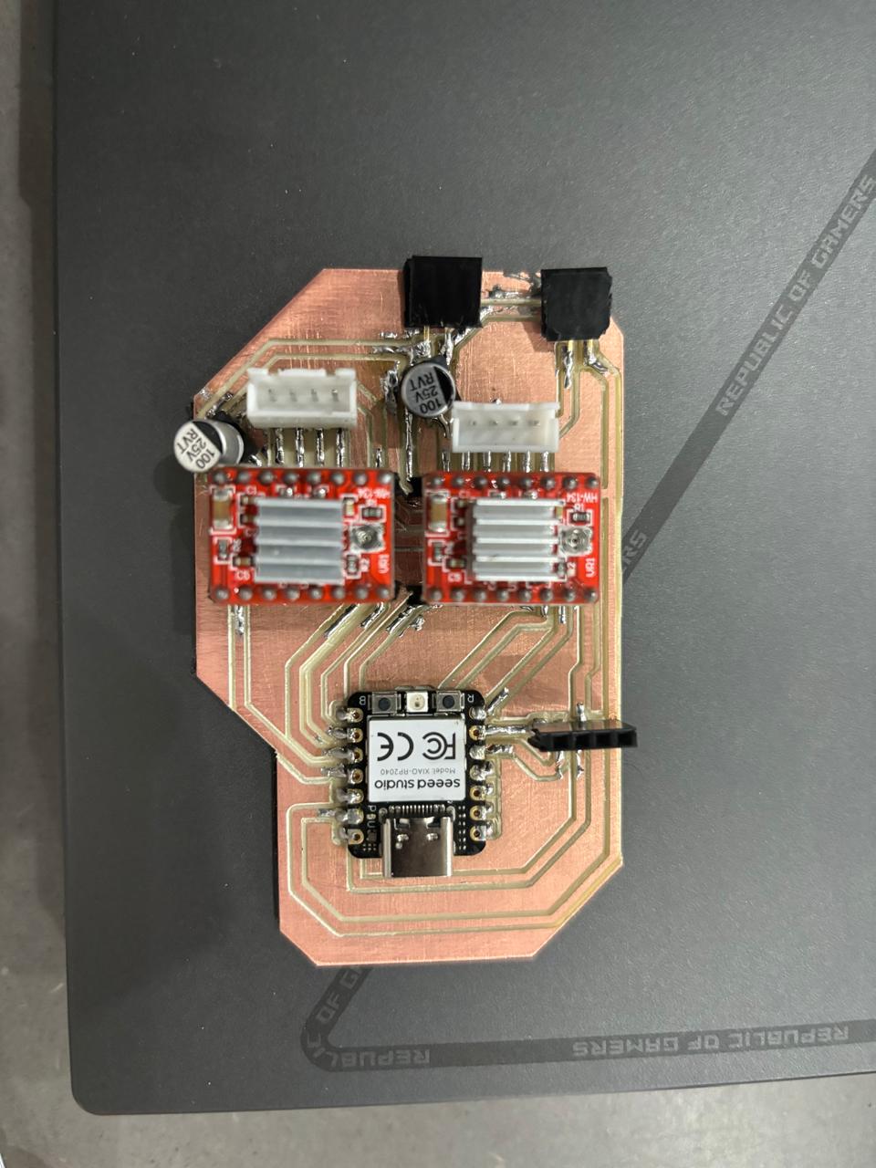
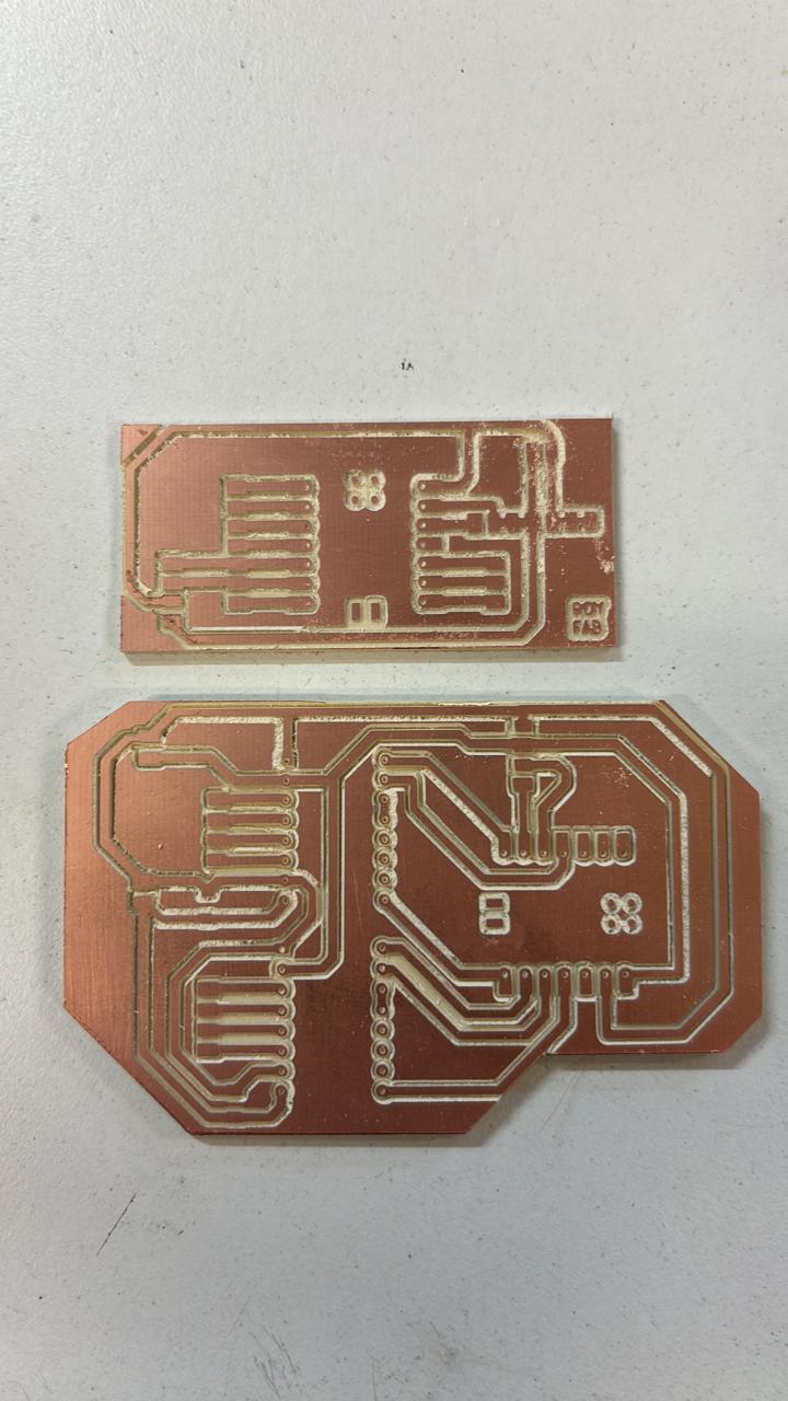
I manufactured a total of two boards in KiCad. These two boards will be used for my final project, as they will be connected to each other to, first, control two NEMA motors or send signals to an LED and a photodiode that will detect movement and position between each of the NEMA motors.
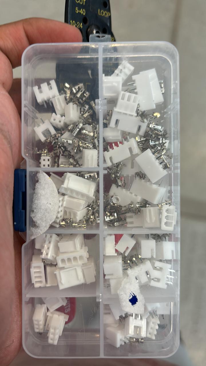
I also adapted several connectors that I found in electronics stores, as I found it easier to use male and female pin headers. This setup allowed me to swap or reconfigure connections between my boards more easily.
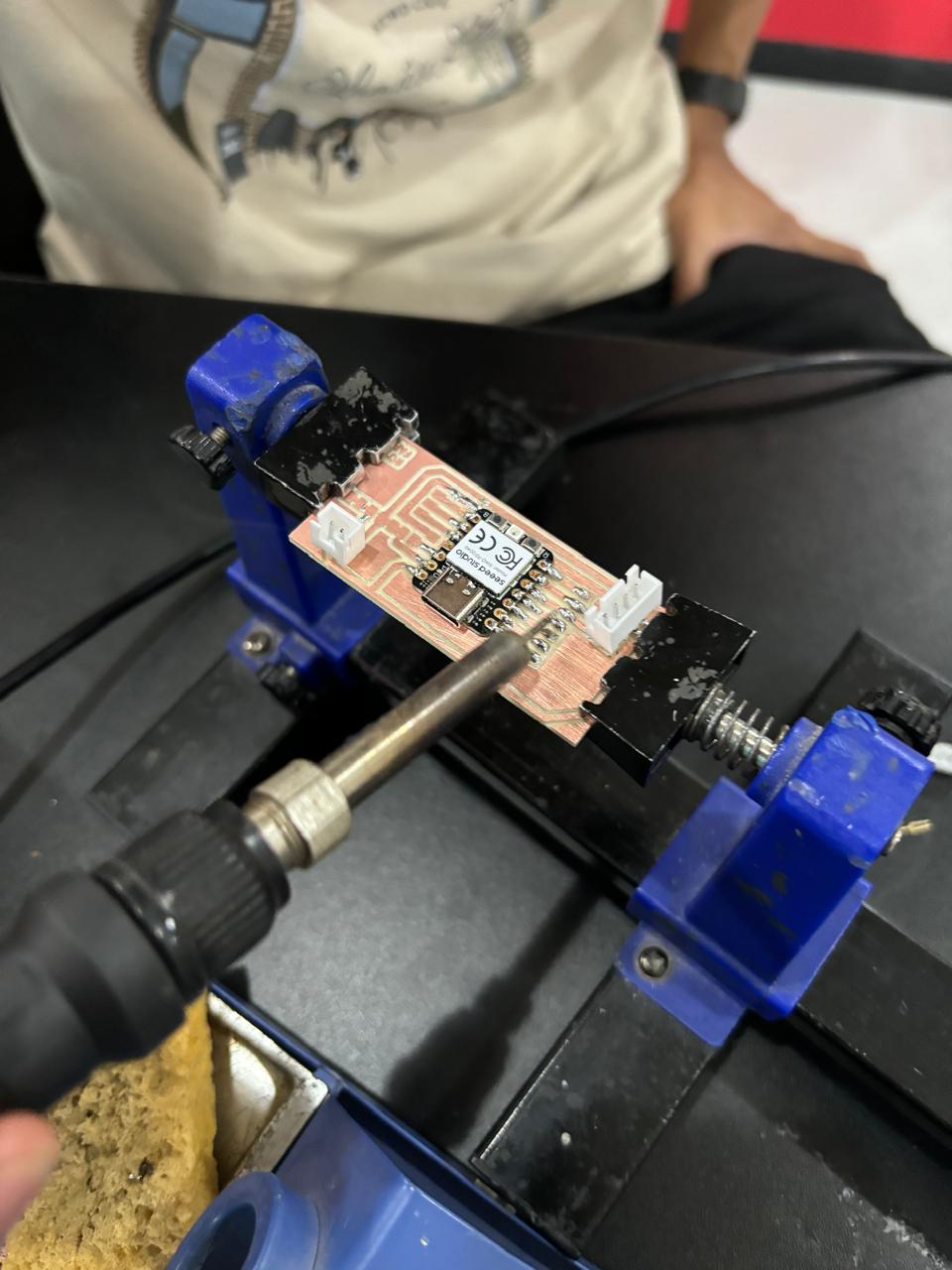
This was my soldering process, where I desoldered the XIAO board that was given to us during the first weeks to create our first board. I then soldered it onto my new board. When I needed different connections or functionalities with these boards, it would be simpler to switch the jumper connections rather than having components soldered directly.
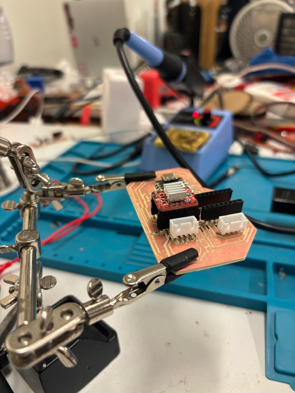
For the connections between the drivers, I grounded them all and added capacitors to the voltage connections to prevent the drivers from burning out. Properly connecting these drivers is crucial, as they are prone to damage. Therefore, I also added male pin connectors so I could easily replace the A4988 drivers if the integrated microcontroller or any of the pins were damaged during the process.
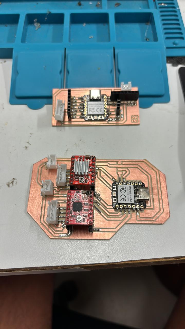
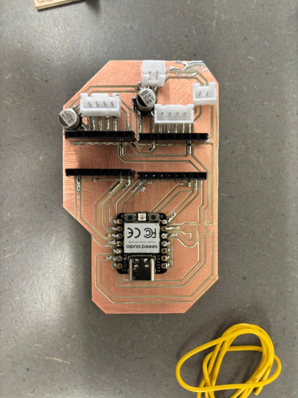
On the second board, I added more inputs and outputs, allowing me to work with TX, RX, and signals such as SCL, SDA, and RESET. I made sure to leave these connections available to avoid any issues in future projects. Below is the connection diagram I envisioned for how my boards would connect. These terminals were designed to support my entire project, as I planned to integrate various components and sensors over time. Therefore, I needed to ensure that at least one board was well-designed and properly distributed to handle multiple inputs and outputs.
