Week 4 Electronics production
In this week i learned how to fabricate a PCB (Printed circuit board) using a small milling machine the SRM-20 this machine is new at my University so for this assigment it was my first experience with it, last works i did it for making PCB's i used one of the Mini CNC we have at Ibero Puebla, i noticed a few things remarkable to write for you, the Roland its extremely expensive for most of the people with 4000 thousand dollars value, and i remember that the value for all of the components in the Mini CNC probably is almost less than 250 dlls, obviously the quallity of the cut in the roland is very clean and you will not have trouble with the traces.
First, I will tell you about the Roland, the mini CNC we will be using this week to manufacture the PCBs. Below, you can see its specifications, and if you want to learn more about this machine, here are the links to my Fab Lab and the official page of the machine.
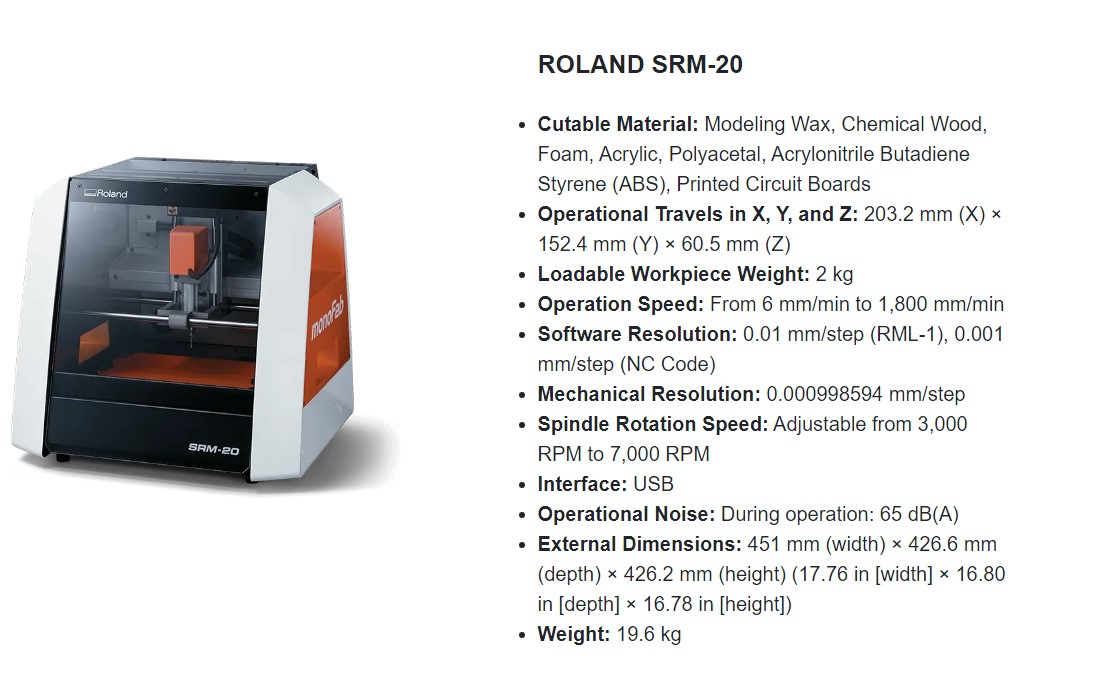
This is the website of the monoFab SRM-20 here
Check our Group Assigment here
A Printed Circuit Board (PCB) is the backbone of electronic devices, connecting components through conductive pathways. The advent of Computer Numerical Control (CNC) milling in PCB manufacturing marks a significant advancement, allowing for precise removal of material to create intricate circuits. This method is ideal for prototyping and small batches, offering high accuracy, repeatability, and the ability to rapidly iterate designs. CNC milling transforms PCB fabrication by enhancing flexibility and efficiency, enabling custom circuit configurations and quick design updates, thus revolutionizing the prototyping process in the electronics industry.

We already know the basics of the machine we'll be using and what a PCB is. Now, join me in completing our task for the week by following the checklist.
AssigmentGroup assignment:
Files
- MODS CE
- ROLAND
- SOLDERING PCB
Generating the files using MODS CE
Steps
Once you made all the steps you will have on your screen the following similar image
Change parameters
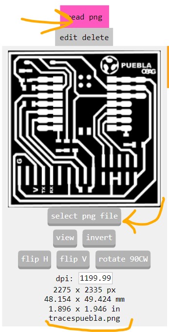
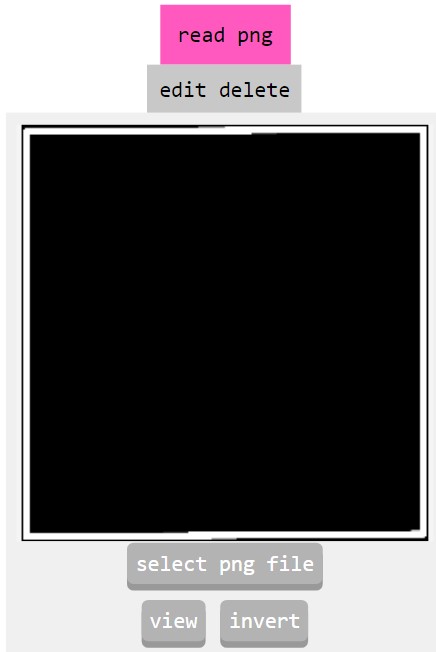
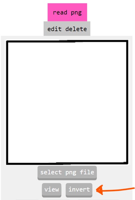
Upload the PNG image
In this step you have to be sure about the image is in black and white (the lines you are going to engrave on the copper board).
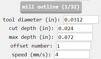
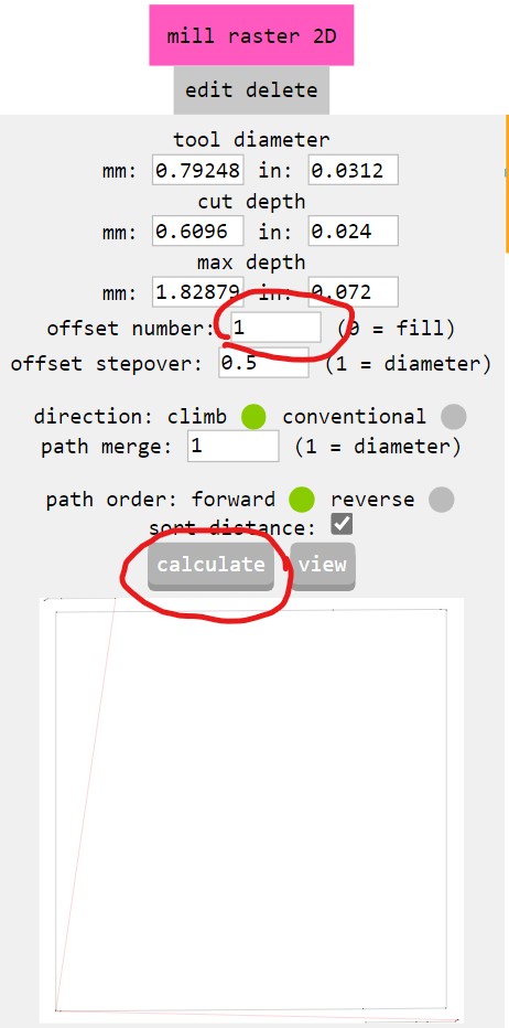
Set traces
The speed (mm/s) is the parameter recommended, because actually the maximum speed is 1800.
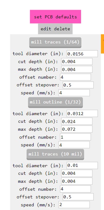
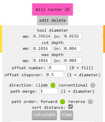
Finally click on Calculate to obtain the file in extension .rml
Aditionally to that, you will have a new tab on your explorer
This two lines are the Offset number
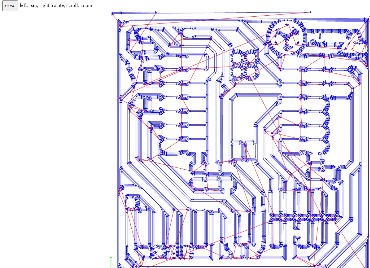
Get the cut file
1. Installing the drivers and software
We need to download and install the softawre Vpanel and the driver
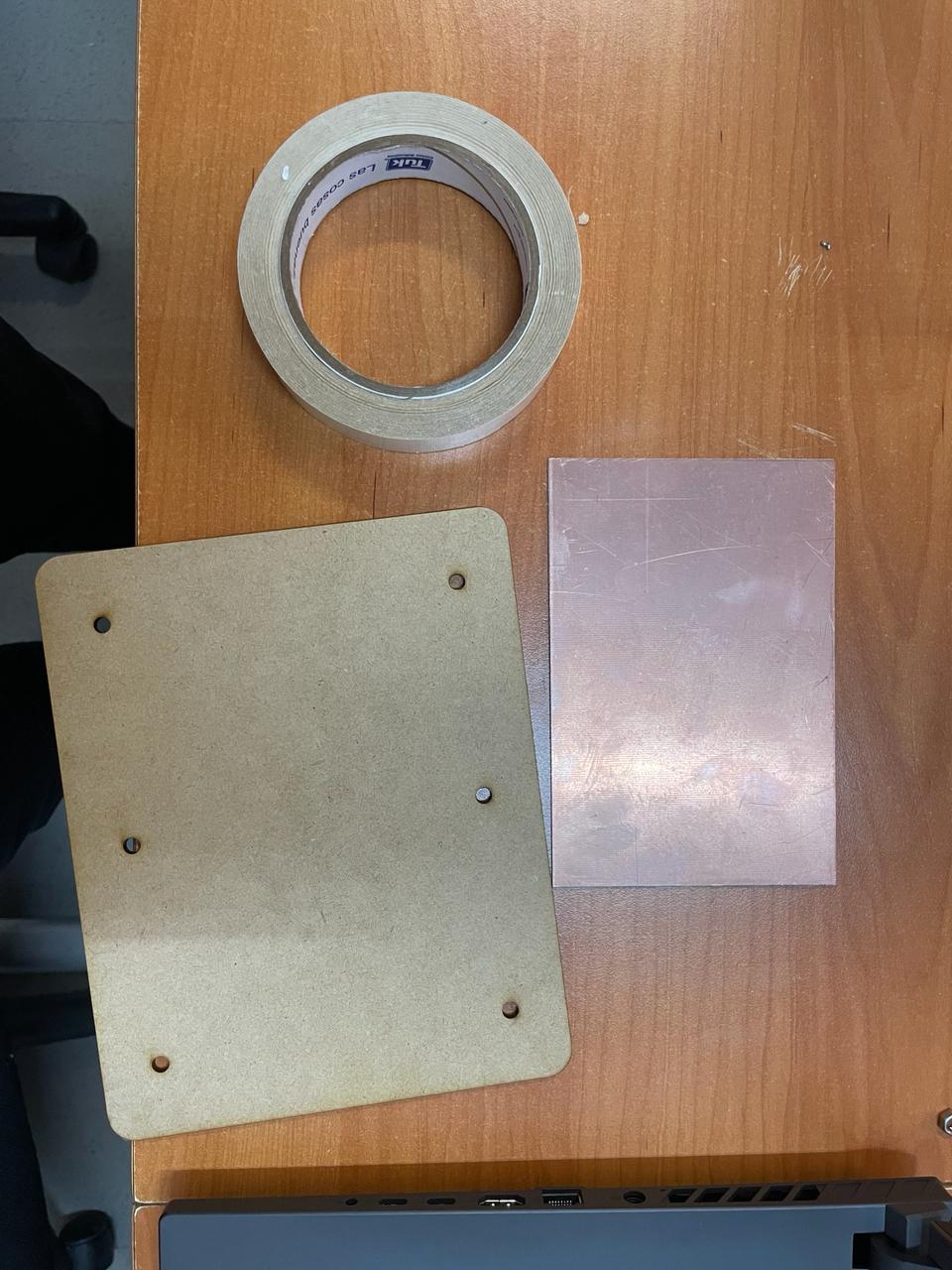
2. Clean and adjust the copper sheet
In this step, we'll need three things. First, we'll require our sacrifice board, which in my case, I cut from 3mm MDF material. This board will be screwed onto the plate inside the Roland. It's important to fasten all six screws to ensure it doesn't move during the engraving and cutting process. Second, we'll need our copper plate, which we must have previously cleaned with isopropyl alcohol. Lastly, we'll use double-sided tape to attach the copper plate to the sacrifice board.
Make sure to apply the tape along the entire plate to prevent any movement during the cutting and engraving process.
3. Software and calibrate the Roland
Now we will install the software and the driver to be able to run the program. It is important to choose the following driver. At the end, I will leave the compressed document for the software download.
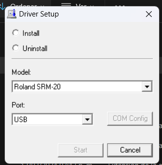
Click on install
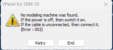
To continue on this step it will be necessary to connect the machine using your port USB, otherwise it will show up the following image
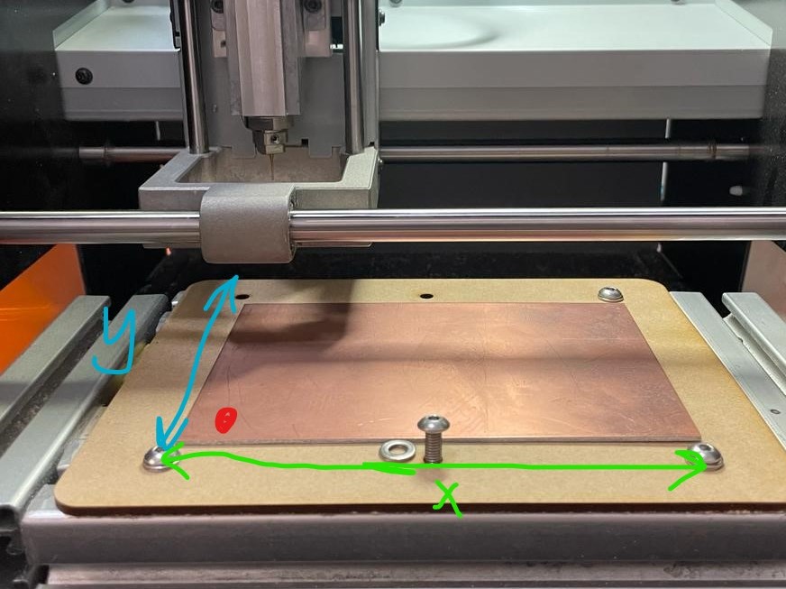
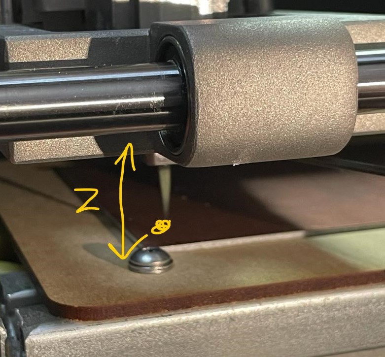
What its Origin Point?
The origin point or machine zero, is the reference point from which all coordinate measurements for machining operations are made. This origin point is essential for the correct setup and operation of the CNC machine, as it determines the initial position of the cutting tool and is used to plan the necessary movements to machine a workpiece according to the specifications of the CNC program.
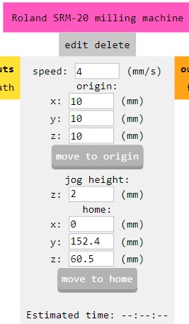
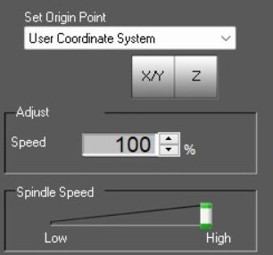
Once connected to the machine, you will be able to open the following interface, where it will be very important to identify the buttons for moving through the X, Y, Z axes. This way, we can modify the starting position of the process.
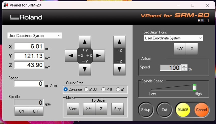
The following buttons are necessary to know; with these buttons, we will define the XY position, and also Z, where we will set the origin point. The origin point is where the machine will start running our program.
Speaking of machine coordinates, it's important to represent them in the 3D workspace, where the X, Y, Z axes are located. Here, I show you a way of how I represent these axes in my mind.
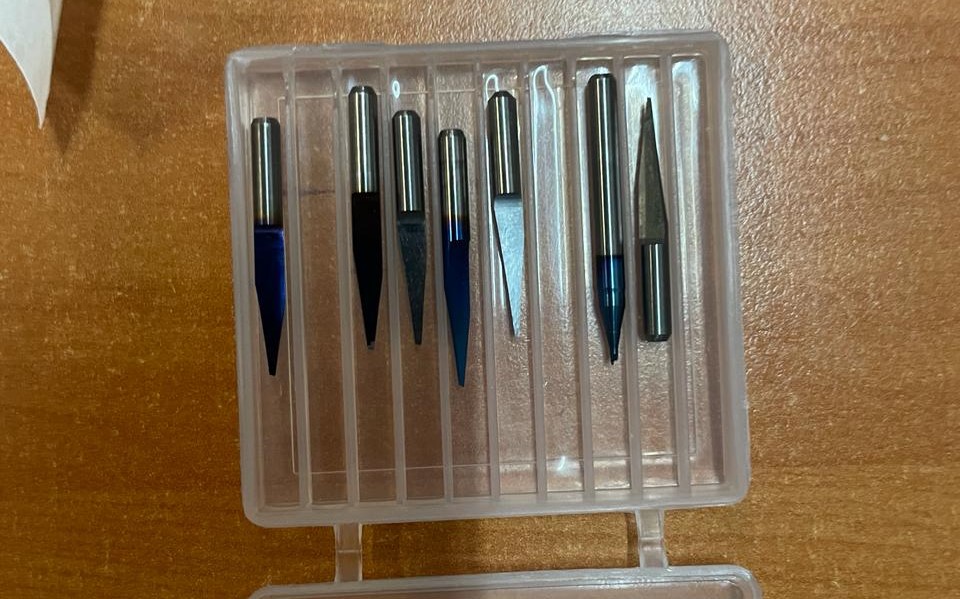
4. Tools and cut
How to change tools for cut and engrave?
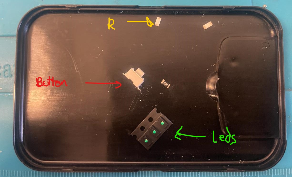
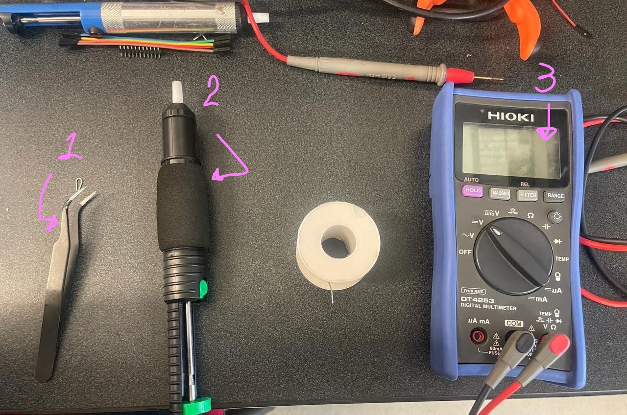
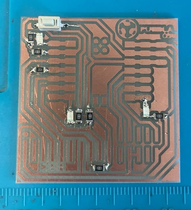
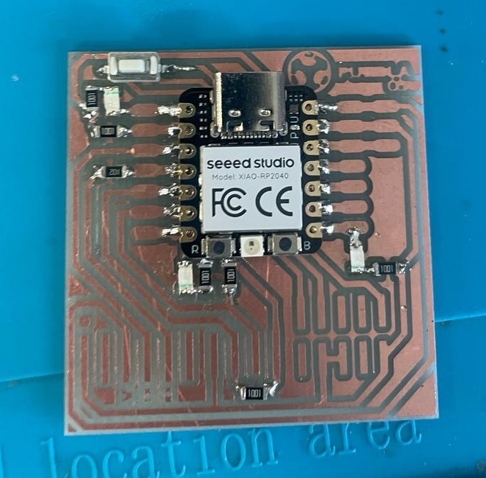
Components
Here are the components i used for making my PCB, are 2 basic components (led and resistance) and 1 microcontroller, you can buy it here
| # | Components |
|---|---|
| 1 | XIAO RP2040 |
| 3 | LED SMD 3518 | \
| 7 | 1K Ohm resistor | \
| 1 | Push Button | \
| - | Tools | \
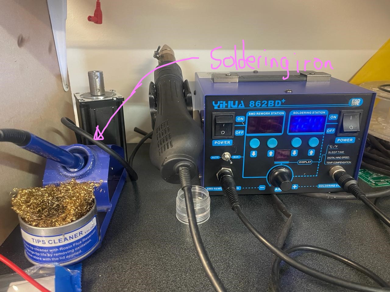
| 1 | Soldering Iron | \
| 1 | Solder spool | \
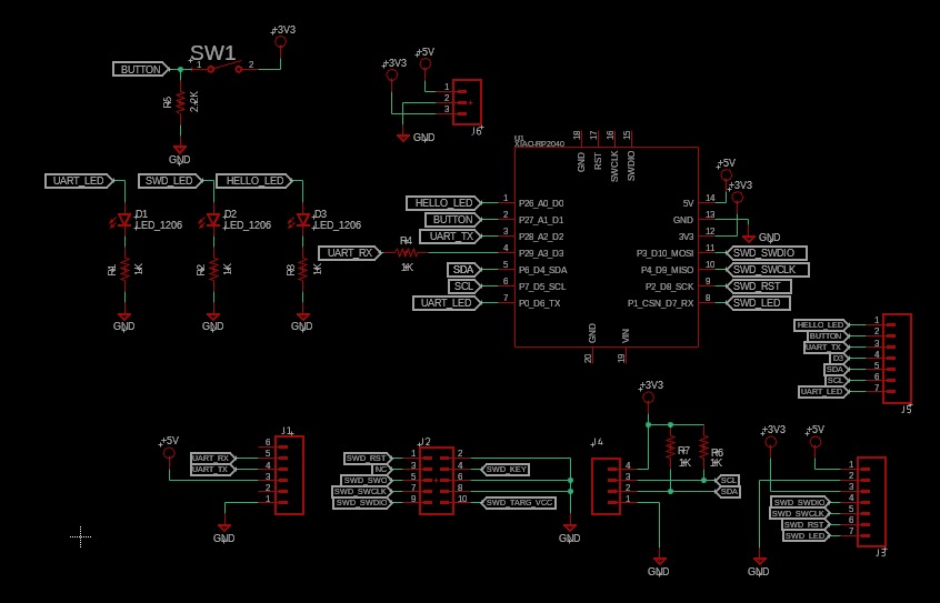
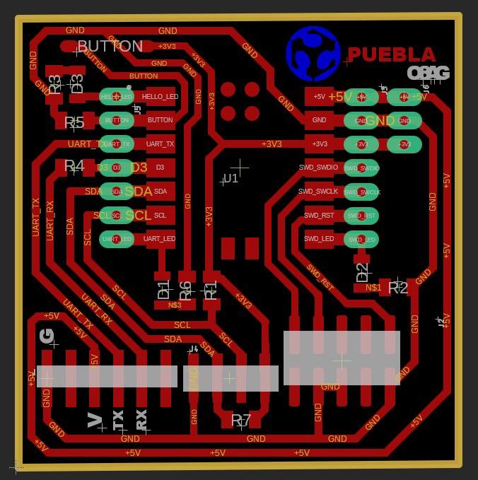
Ki Cad
These following two images are the design of the pcb previously of the engrave work with the copper sheet, the first one is the schematic where are connected all the components to the microcontroller (Xiao), basiclly are two interfaces in Ki Cad for designing a PCB, the schematic interface and the other one where you can move all the traces, in the first one you select which components you are going to use, how you are going to connect and how many there will be. In the desisning traces part you will be able to move all around and where you like. Additionally, you will be able to edit the colors and the thickness of the tracks, in this way you will be able to differentiate which can go on one side or the other, as well as see which are connection paths or ground paths."
Soldering
It is my 10th semester studying Mecatronics Engineer, so i already had experience soldering things, i recommend you the following video to learn how to do it correctly.
i recommended to solder first all the resistances > leds > switch button
Use the PCB design to guide yourself and look where it find each component, also i'll give you some tips:
At the end the microcontroller, you will face this step in two ways, very hard o too easy ha. What I did was leave the solder on the tracks where the XIAO pins would be located. Once the solder was left on the corresponding tracks, all I had to do was heat each track to melt the solder so that it would rise to the XIAO pin.
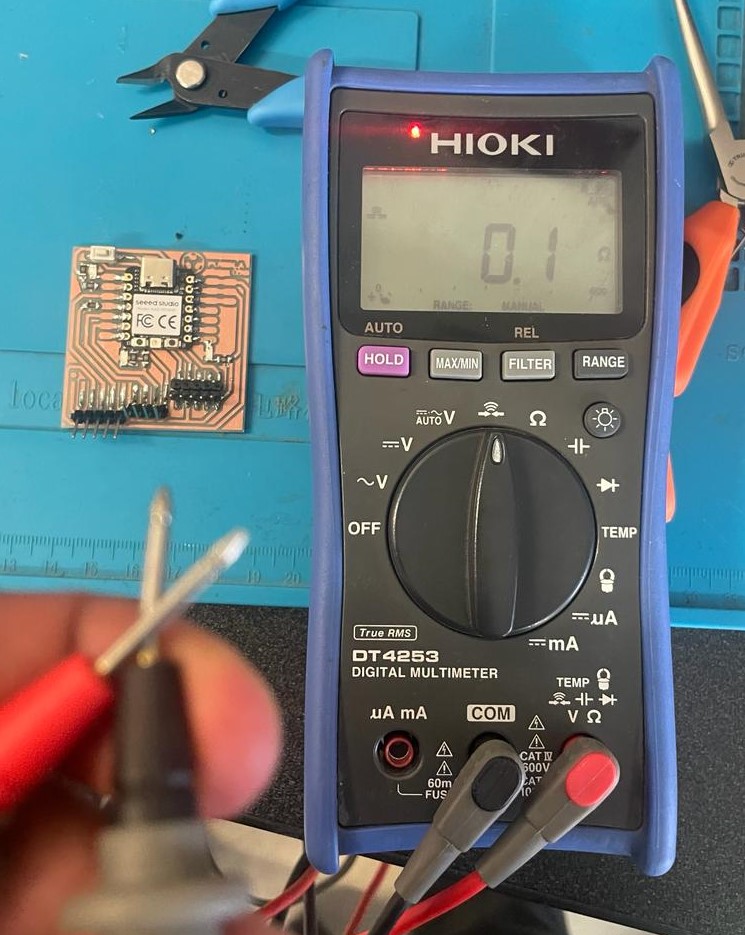
Dont forget to use the multimeter to corroborate the pins are well connected with the pads and traces using continuity option which is the middle one.
Source code
Test
FInally its time to upload a programm to check is working correctly our PCB, to do that i upload a blink program on arduino, those kind of programms are examples on arduinos library. This is the code i used.