Electronics Desing
The assignment of this week was to design a board using any EDA software.
EDA software - KiCad
An EDA (Electronic Desinf Automation) software is a software focused on the design and production of electronics systems, going from integraded circuits to the development of printec circuit boards. To design my board, although I already have experience with Fusion 360, I used the software Kicad beacuse it was the one our instructors recommended and taught us.

Kicad is a free open-source EDA software that feautres schematic captura, integraded circuit simulation, printed circuit board (PCB) layout, 3D rendering, and plotting/data export to numerous formats. It also includes high-quality component library featuring thousands of symbols, footprints, and 3D models.
Libraries
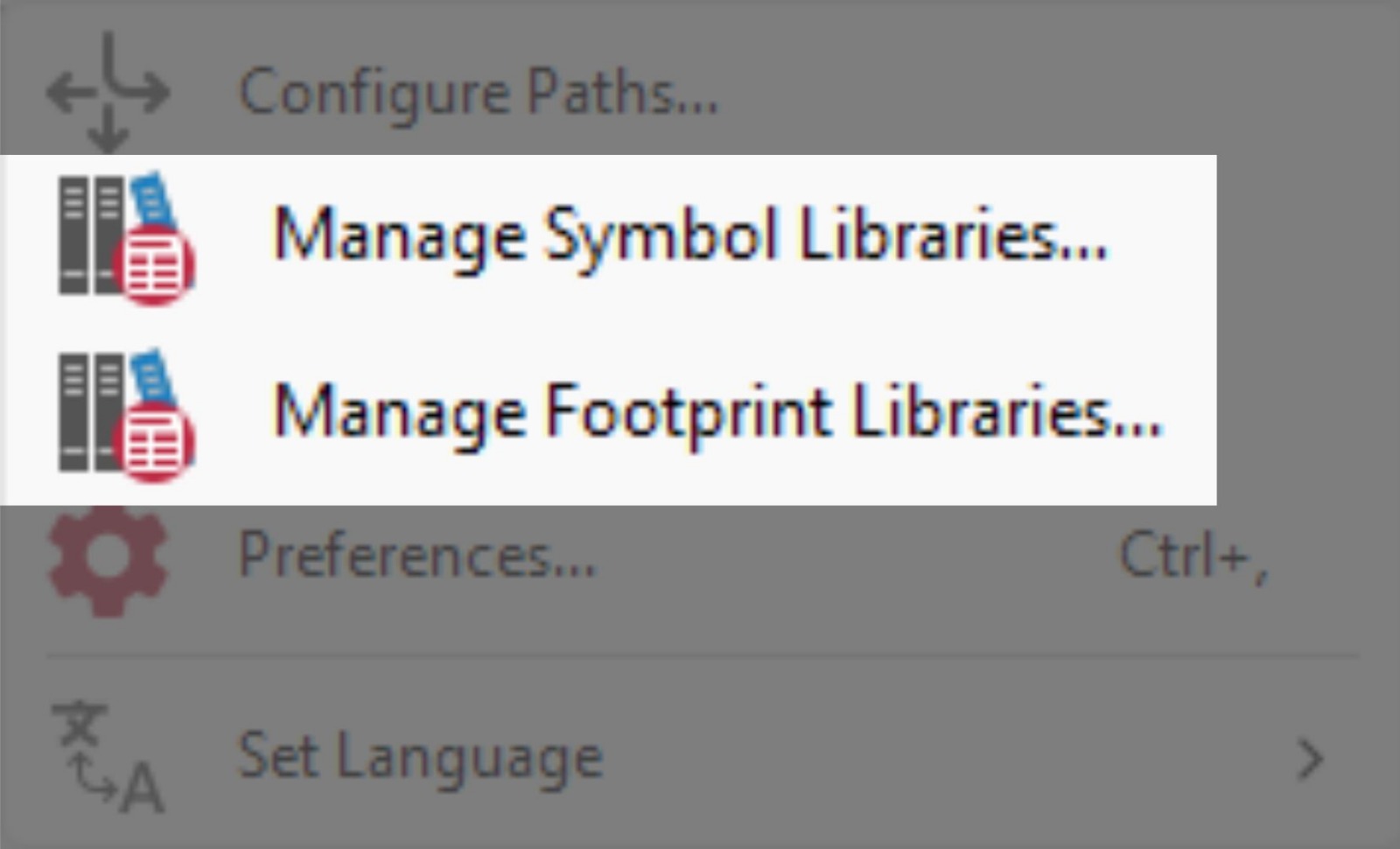
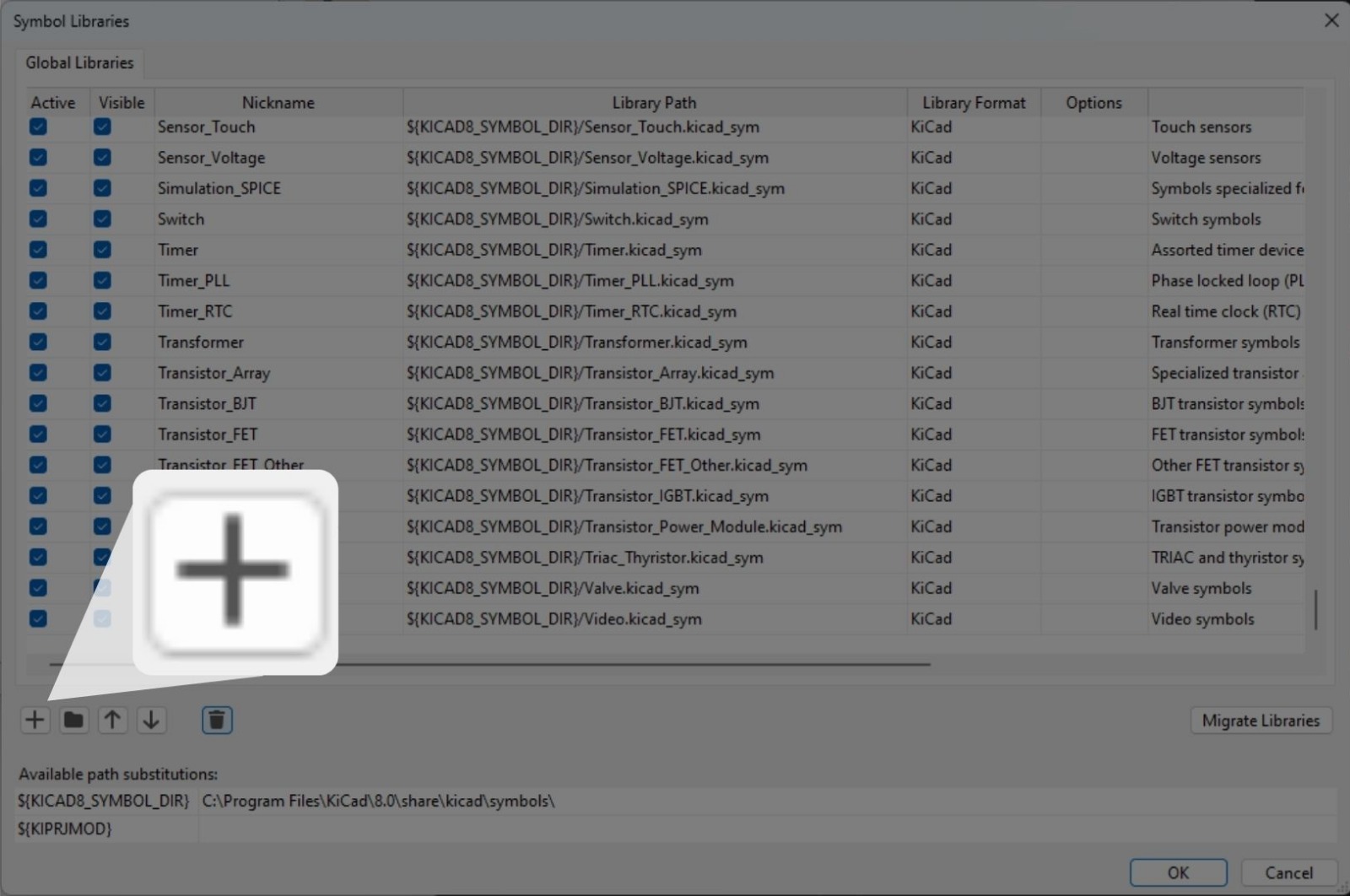
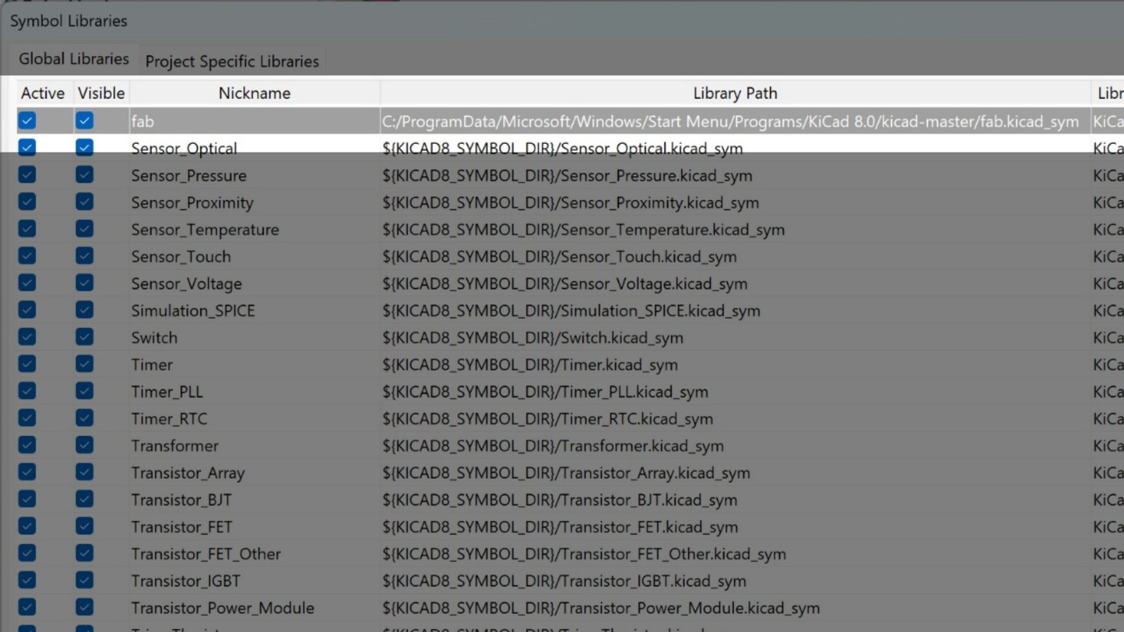
To make the pcb design easier, our instructors gave us a library that just includes the components we have here, we jus needed to add this library on KiCad.
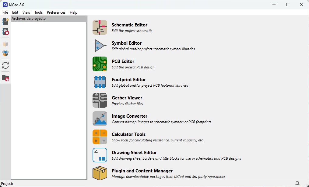
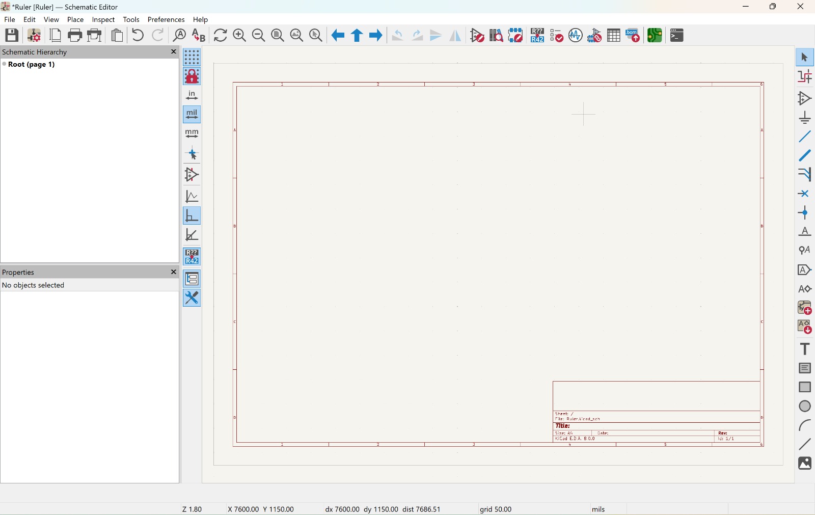
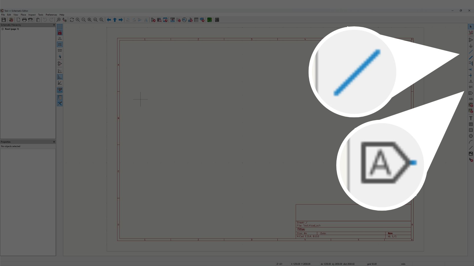
The first think you will see when KiCad opens is this, from this, follow the next steps to add the libraries.

Schematic
Now that I have the library with all the components I can use, it was time to create the schematic of my board. To open the schematic file go to the "File" and select "Projet". After that, you will end up with this on your screen.
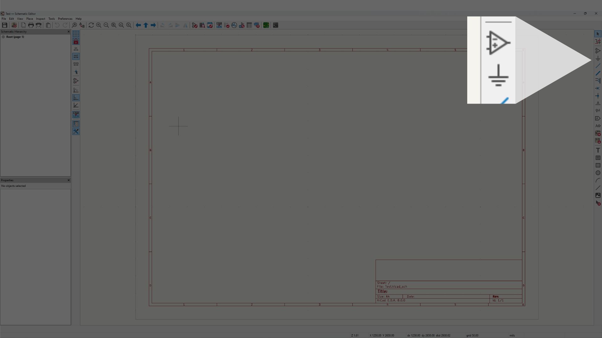
To place things on the schematic we have to buttons, one to add the symbols and the other one to add the power symbols. Once you select it, you just have to search for the component you are looking for and place it.
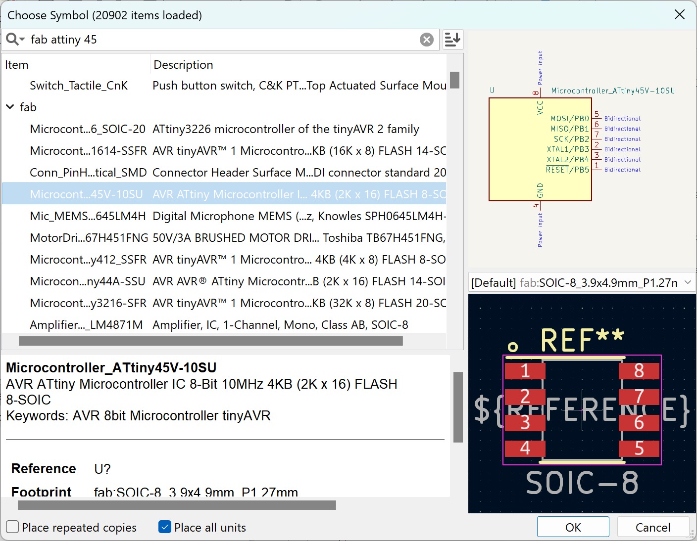
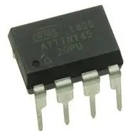
Something I recommend is to pay attention of the components you are using, there a lot of them and it can be easy to confuse them. For example, I used the wrong attiny 45 and it gave me a lot of problems while soldering.
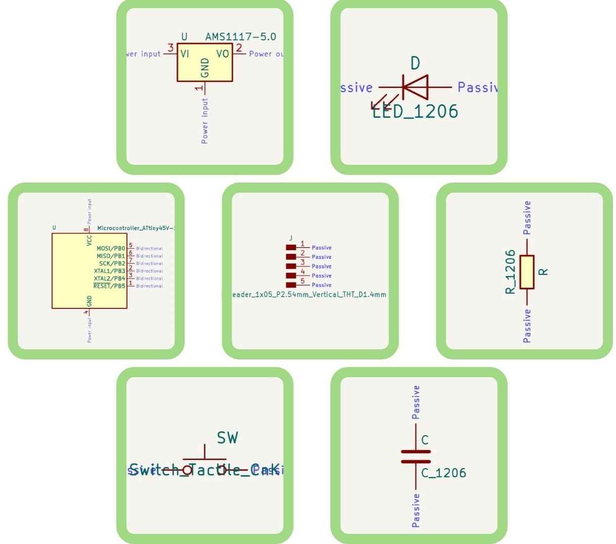 The components in general that I am going to use are the following.
1.- Attiny45: The microcontroller.
2.- Voltaje regulator: In case I use a battery.
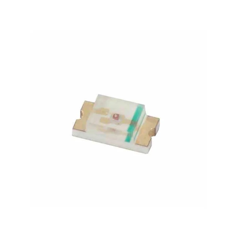
3.- LEDs
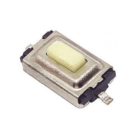
4.- Buttons
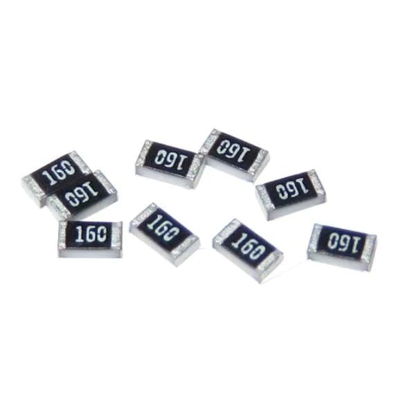
5.- Resistors
6.- Capacitors
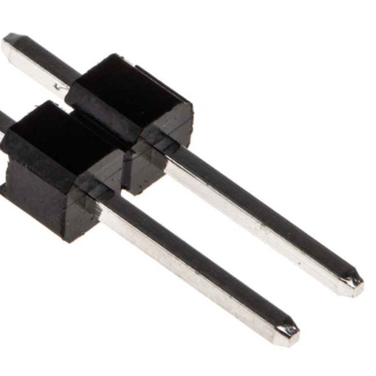
7.- Pinheaders
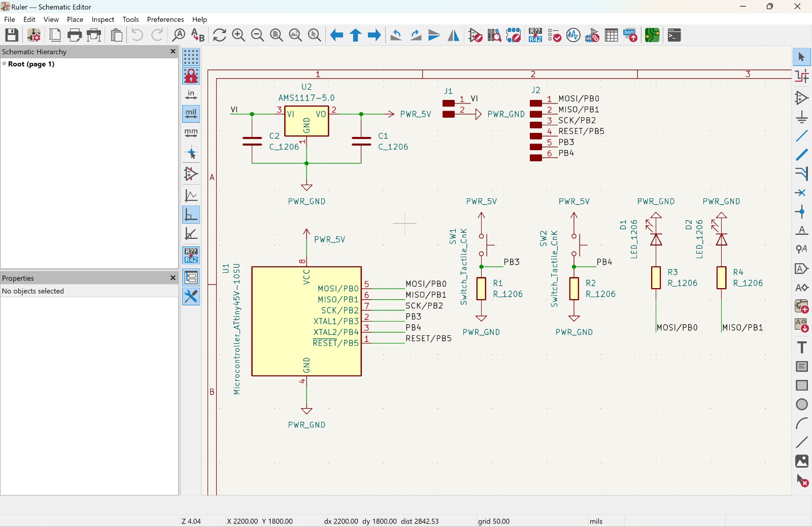
Once you had all the components it is time to connected, there a two tools for that, the ware to make short connections, and the label, it is the same as a connection but cleaner.
Here is the result of the schematic:
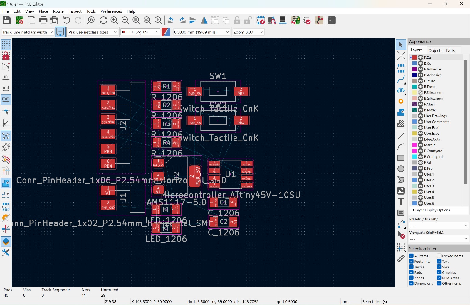
PCB Editor
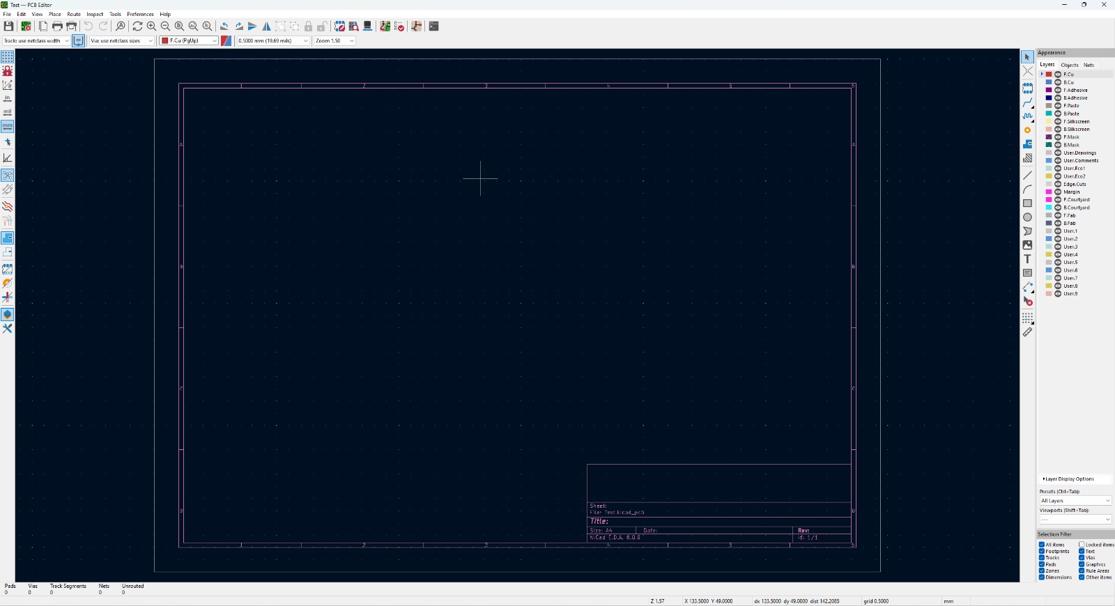
Once I have all my compotents on my schematic it was time to create the PCB. First of all we have to open the PCB file. To do that just press the following button and it will open you this window.
We have the file but there are any component we have on the schematic, to add them go to preferences and click on "Update PCB from schematic" or just type F8.
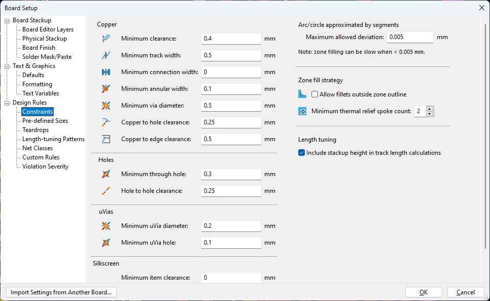
We have to move the components on a convenient way and route them, but before that we have to define the rules that our paths need to have. To do this we go to File 🡢 Board Setup, in here we go to Constraints located in the Design Rules section. We modify the Minimum clearance to 0.4mm and the Minimum track width to 0.5mm. We modify this width depending on how much amperage we need, a bigger width will make more current flow, the components I am using does not need a lot of ampere but I choosed this parameters to play it safe.
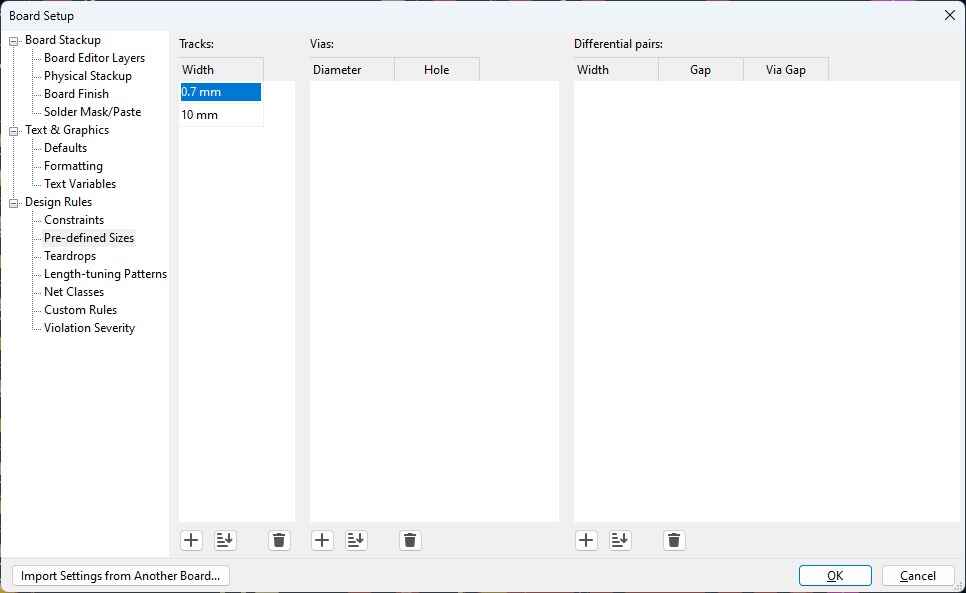
Also on Pre-defined Sizes add a track width of 0.7mm.
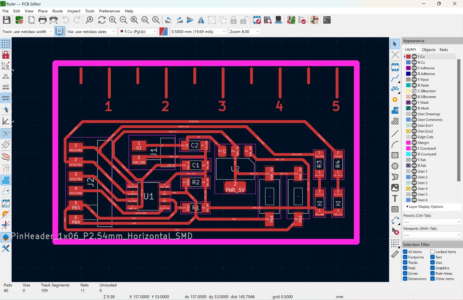
We also have to know the different different tools we have. The first one is the Route tracks, this tool will help you connect the components and make the track between them. There are also tools to draw lines, rectangles and circles.
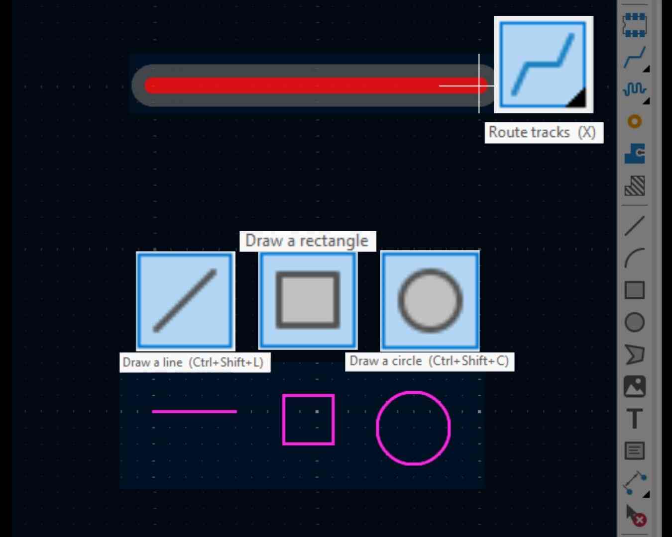
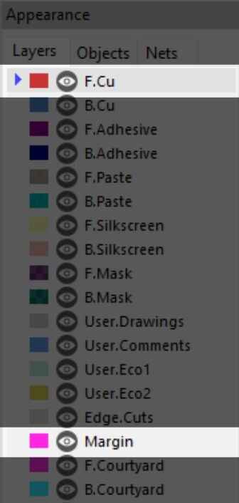
As you saw in the previous image, the color of the lines were different, this is because there are also different layers where you can draw. Each layer has its purpouse, the F.Cu layer (the red one) is the one where we are going to draw the tracks and thing we want to trace and the Margin layer is where we are going to draw the lines we want our mill machine to cut.
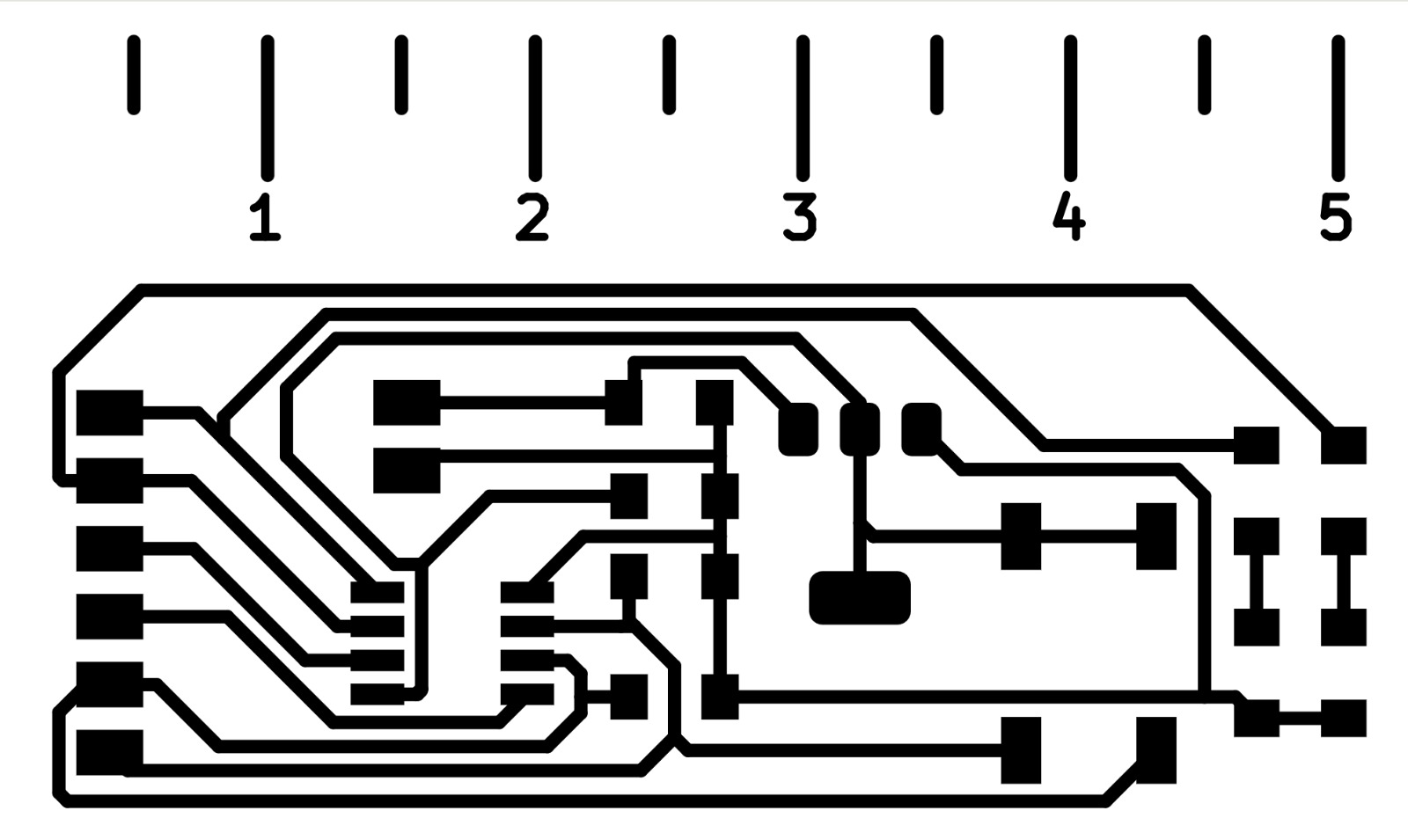
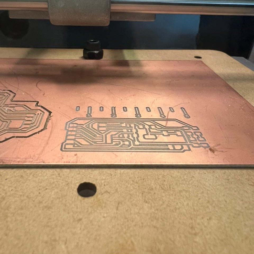
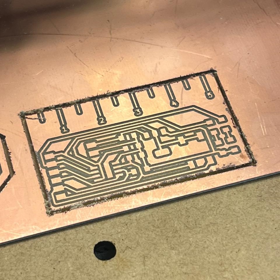
An idea that came to my mind was to desing a little ruler on the PCB to measure little things and after spending a good amount of time I finally got it. As you can see, the cut lines are thicker, this is because I
Once the design is ready we have to save them as SVG files, to do that go to Files 🡢 Import 🡢 SVG. Remember to set the Print Mode in "Black and white" and change the SVG page size in "Board area only".

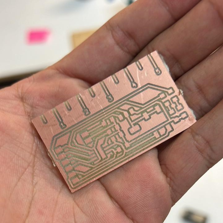
Milling and soldering
Milling
A problem all of us was that the schedule to milling machine was full, and very tight between one use and other. So what a friend and I did was to share the same schedule and mill our pcbs at the same time.
To use the mill machine I followed the steps of the Week 4 assignment.
Soldering
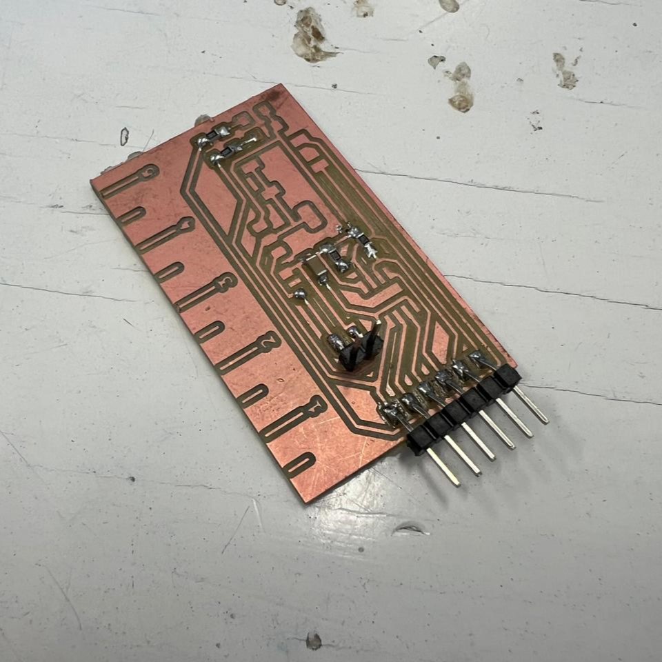
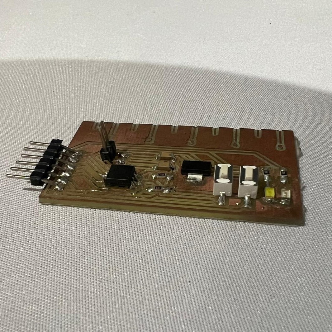
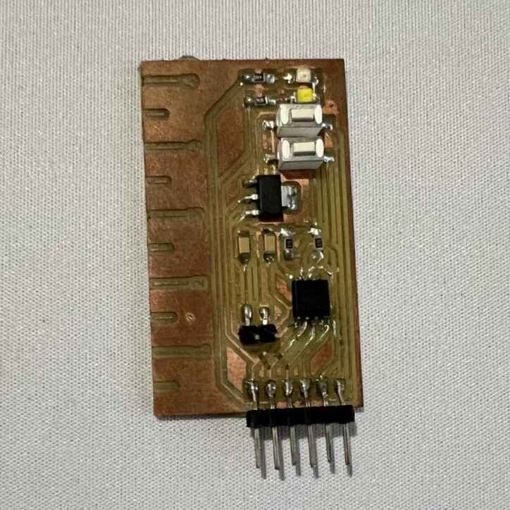
First of all, I had to get the componnets that I am going to solder.
| Material | Quiantity |
|---|---|
| Attiny 45 | 1 |
| Push button | 2 |
| 2.2K Reistor | 2 |
| 1k Reisitor | 2 |
| LEDs SMD | 2 |
| Pin headers | 8 |
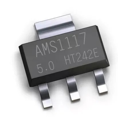
| Voltage regulator AMS1117-5.0 | 1 |
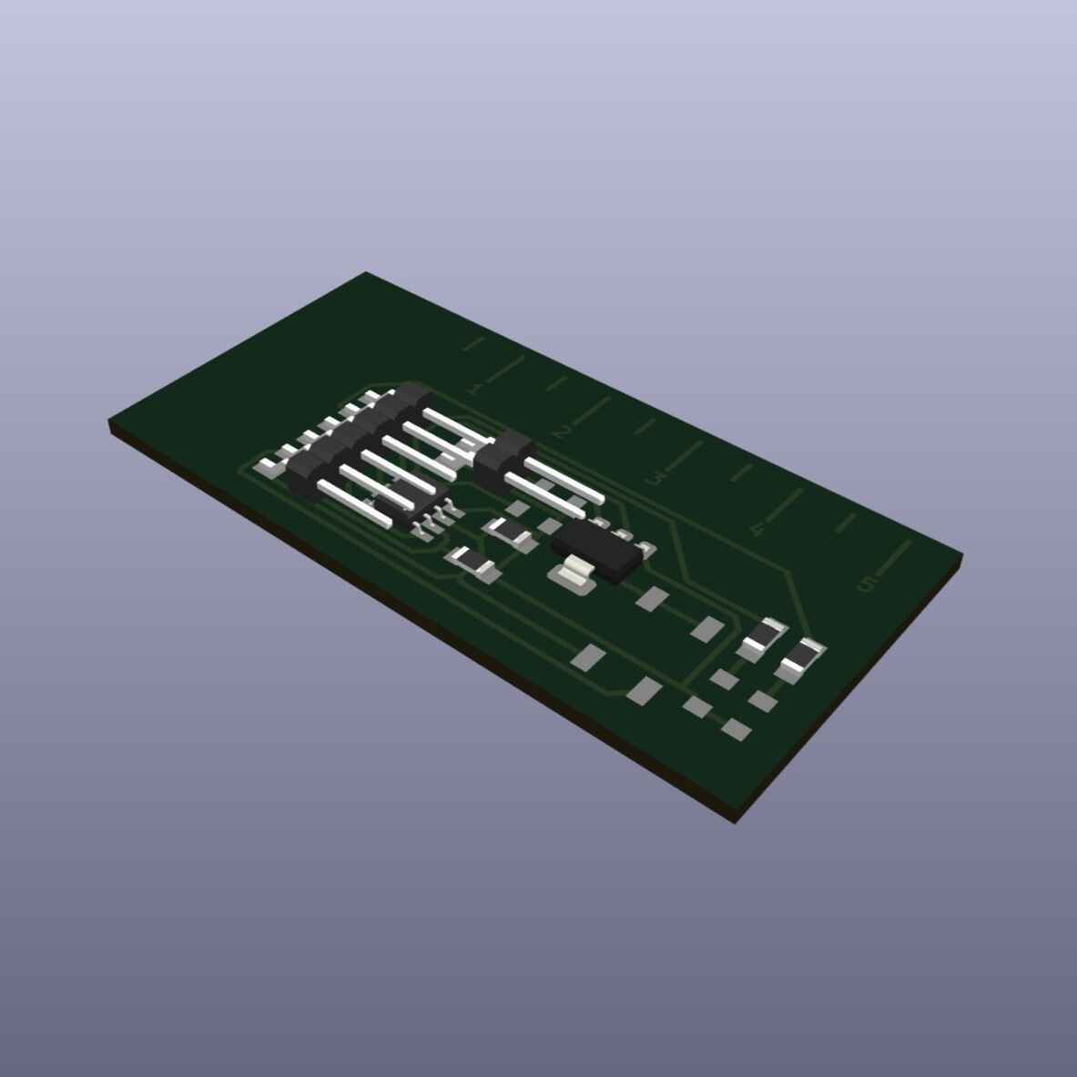
Although it was my second time soldering, I think I did it pretty good, expect for something...
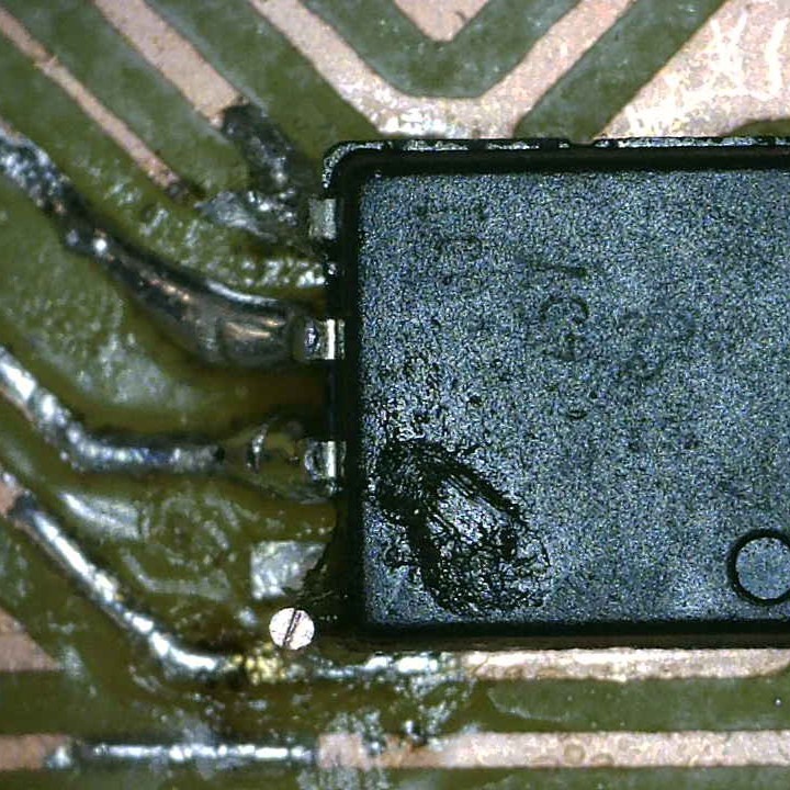
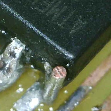
I used the wrong footprint off the attiny 45, I had to bend the pins so they can fit, this making the solde harder. Because of this, I ended up breaking the Voltage pin, something I had to fix using a wire.
Aside from that, everything else was good.
Testing
Beacuse I had to use the attiny pins, first I needed to test if every connection was fine, to do that I used the multimeter and used it the way we learned on our group assignment.
Programming process
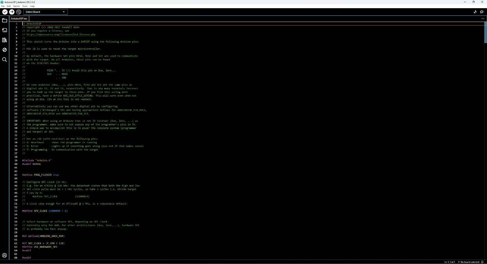
Fortunately, everything was in order. To test it I used and arduino uno as a ISP, our professor Huber gave us a step-by-step guide to change the Arduino into an ISP.
First of all you have to download the library using this link https://raw.githubusercontent.com/damellis/attiny/ide-1.6.x-boards-manager/package_damellis_attiny_index.json.
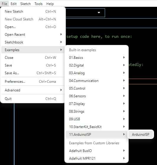
Then, we open the example of ISP and upload it to our Arrduino uno.
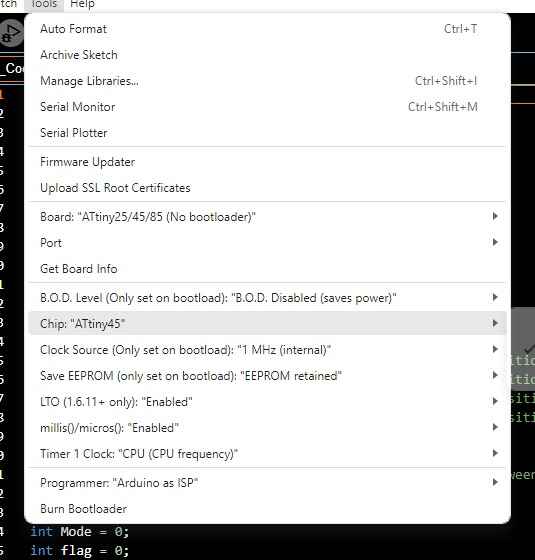
Finally we use the following configurations (change the chip depending on what attiny you are using).
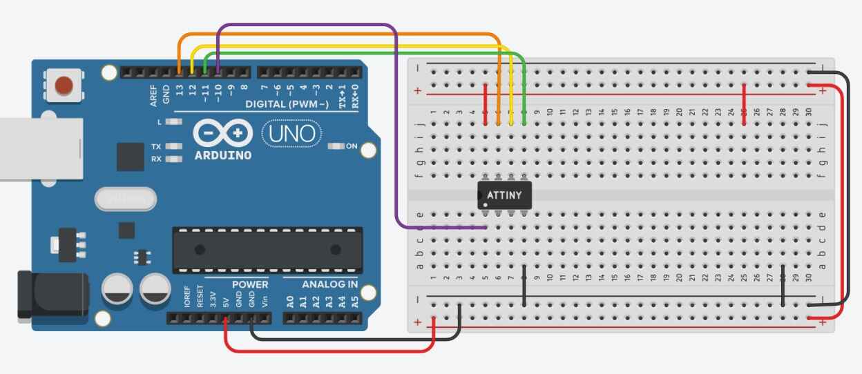
Here is an schematic of how yiu have to connect the attiny you your new ISP programmer.
More information about arduino and libraries is in my Week 4 and Week 6 assignments.
To test the pcb I used a blink code, something simple.
	void setup(){
		pinMode(0, OUTPUT);
	}

	void loop(){
		digitalWrite(0, HIGH);
		delay(100);
		digitalWrite(0, LOW);
		delay(100);
	}