8. Electronics Design
On this week I learned to design a PCB using the software KiCad. KiCad works creating the circuit diagram and then designing the PCB. For this week it is necessary the KiCad software that you can download here, some previous knowledge from other weeks (in specific week 4 and week 6) and extra information for the PCB design that you can find on the group's website here. I designed a PCB that works with an Attiny44 that I will probably use on my final project.
KiCad Setup
Now, I am going to explain how to use KiCad explaining the most useful tools and settings. Before running the software, you should download and install the libraries necessary for the FabAcademy. To download the libraries, you can click here. Now that you have the library, you can run the software and install the library. To install the library, we have to follow these steps:
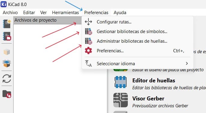
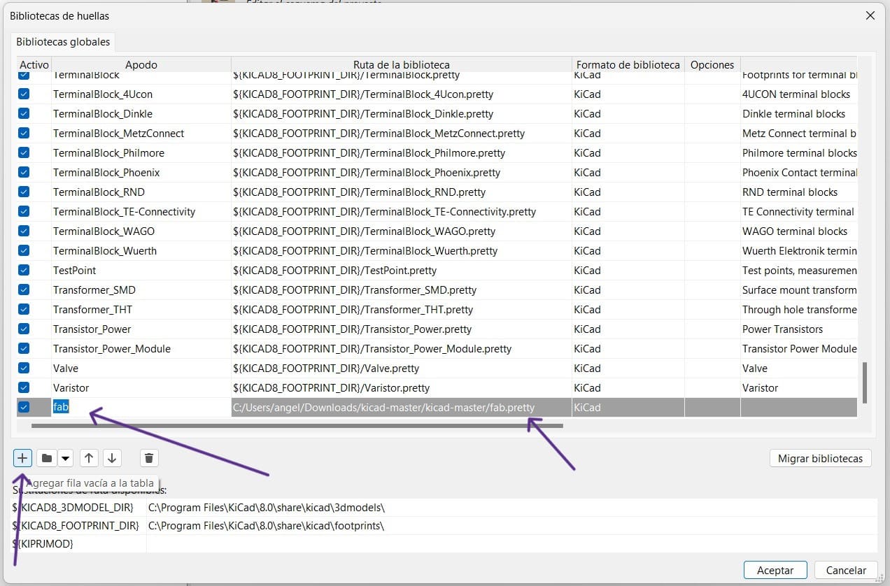
First, you need to open "Preferences" and click on "Manage Footprints Libraries". After clicking that option, a window is going to appear showing the footprints that came with KiCad. To add a new footprint, you should click on the "plus" button, name the footprint with the name "fab" and add the ".pretty" file of the downloaded library:
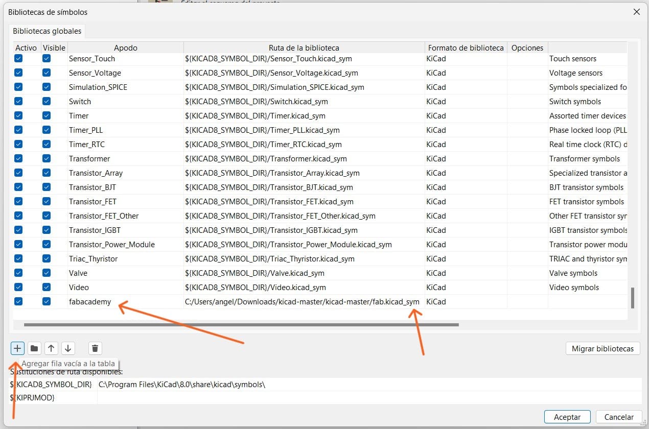
Then, on the same section ("Preferences"), you should click on "Manage Symbols Libraries". After clicking on that option, a window will appear and you should repeat the same adding process, but instead of adding the ".pretty" file, you should add the "_sym" file.
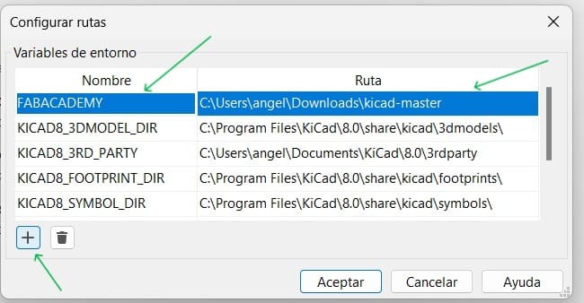
Finally, it is time to install the paths. To do this, you should click on "Set Routes" and follow the same adding proccess, but in this case, you are going to add the whole library folder:
kicad schematic
Now that KiCad is ready to use, it is time to create the schematic of our PCB. This is how I did it:
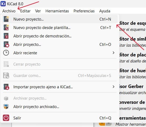
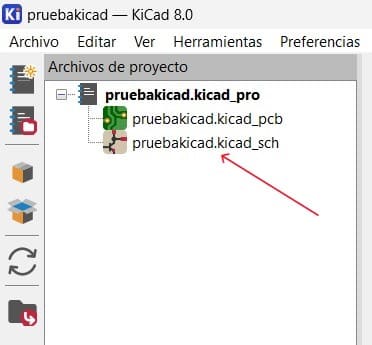
- Create a File: The first thing I did was create a new project on the "File" section. Aftes clicking on "New Project", I chose the location and the name of my file. Now that I created a new project, two different files will appear, the first file to modify is the "_sch" file. To open this file, I clicked twice on the file name.
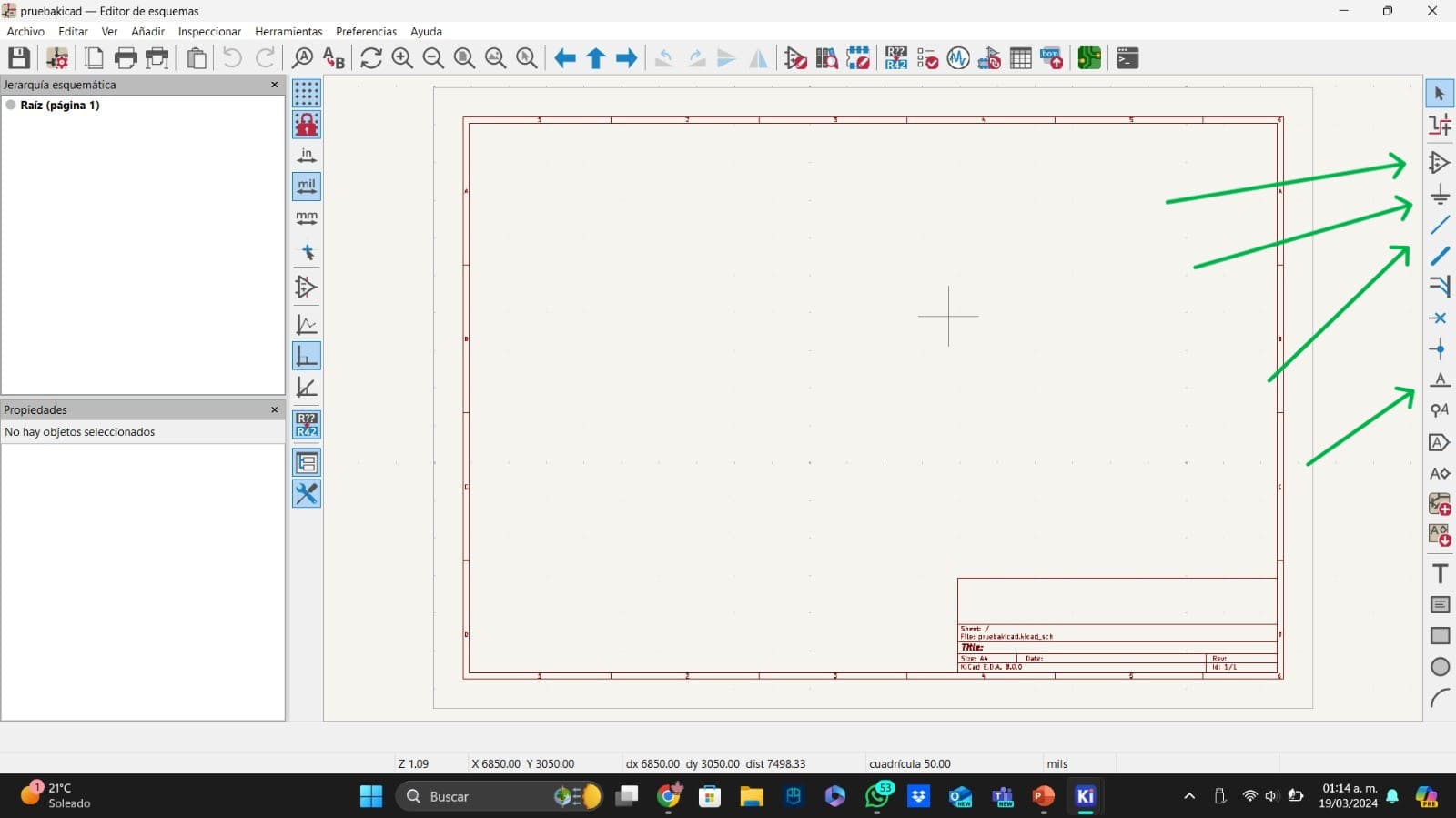
- Sch Main Page: Once on the schematic, we will see an empty sheet with a toolbar on the rigt part of the screen. The marked tools on the image below, are the most useful ones and the ones I used for my PCB.
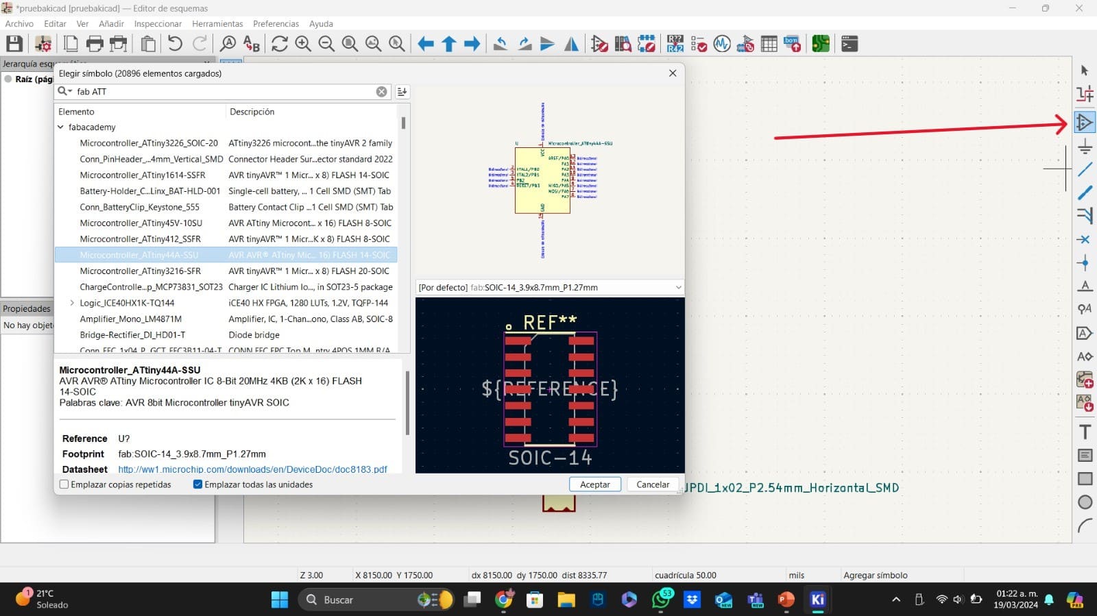
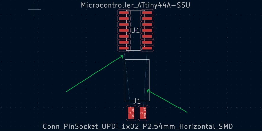
- The Components: One of the tools that we can find on the toolbar allows us to select components and put them in our workspace. On the selecting component window, we can see how the component looks in the schematic and how the footprint will look on the real PCB. For the FabAcademy is important to use SMD components, you can check the component footprint to make sure it is the SMD version of the component (the footprint won't show any hole).
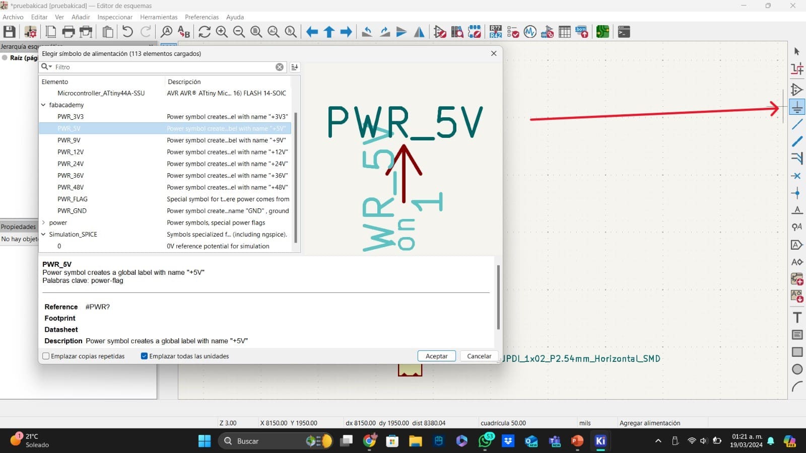
- Ground and Power: Similar to the tool above, we also have a tool that allows us to select and put only different voltages and ground. We can use this tool to connect drectly all the components that need voltage and ground.
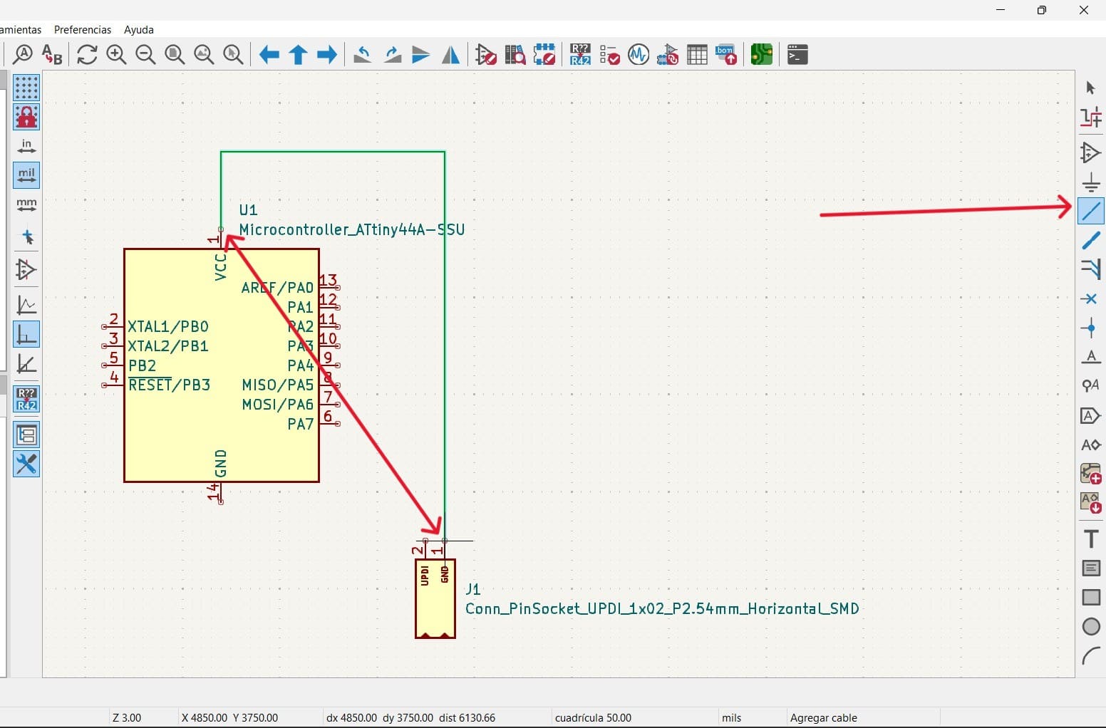
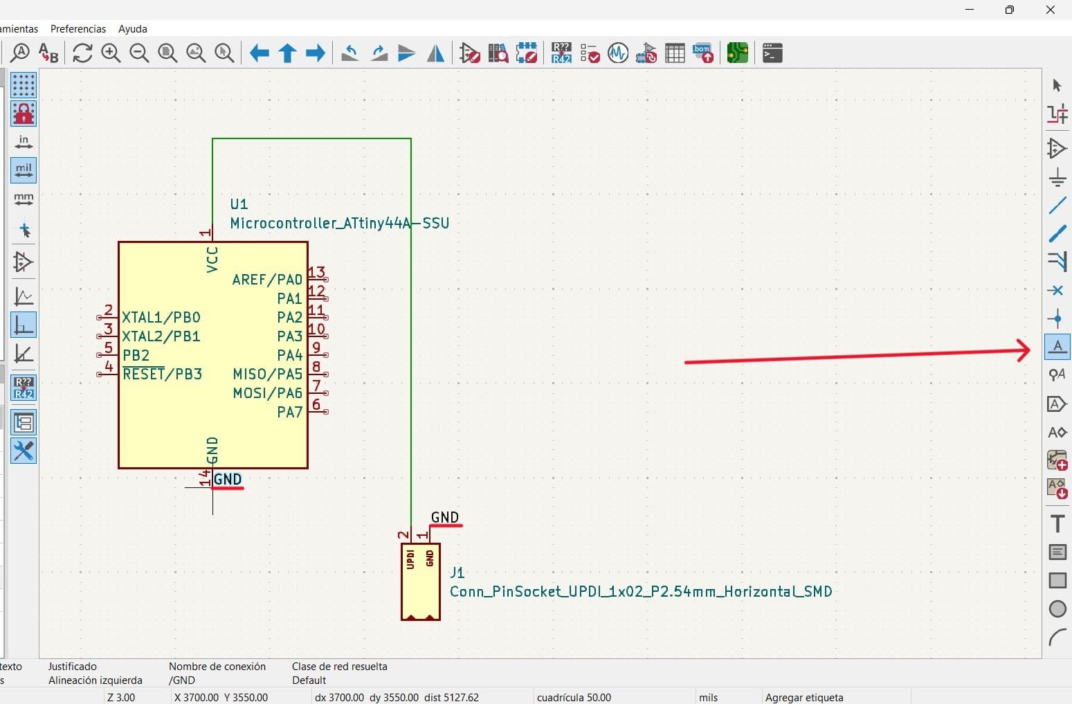
- Connections: Now that we have all the components and the power con the schematic, it is time to connect them. To connect the components, we have 2 options. The first one, is using lines that looks like a real wire, this option is recommended for components close to each other. The second option is using the same word to connect each component (this option connects all the pins that are connected to the same word), this is recommended for components far to each other or when the schematic is too complex.
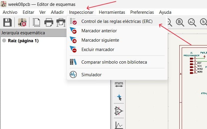
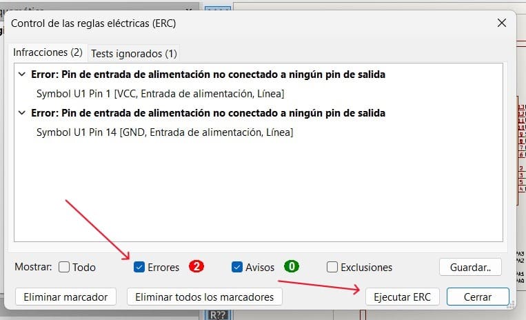
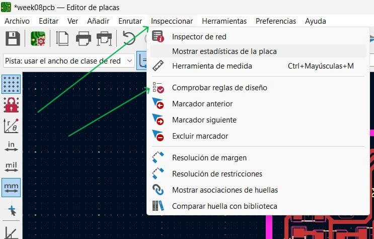
- Checking Erros: Once the schematic is finished, it is time to check possible errors and warnings on the diagram. To do this, we go to "Inspect" and then on "Electric Rules Control". After running the ERC, you will see your errors and warnings, some errors are not important or are not useful things, so you should evaluate which error matters or not.
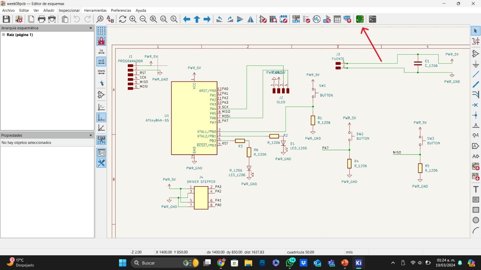
- From SCH to PCB: After finishing the schematic, it is time to pass the schematic to the PCB. On the PCB is where you are going to make the real connections that you will have on the real PCB, so it is important to have your schematic full and functional. If you have any questions about how to connect any component, you can search for it on internet.
The next image is an image from mi schematic. I am going to explain my PCB:
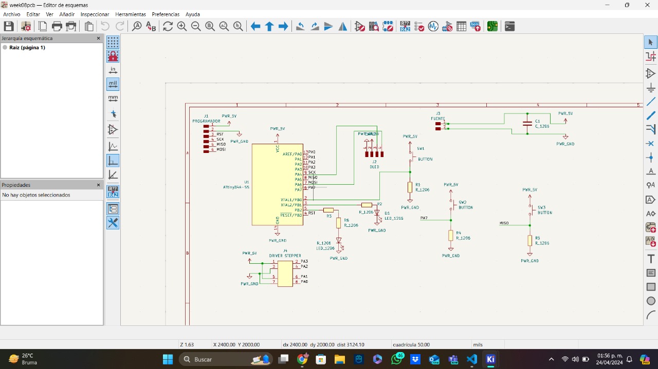
In this PCB schematic, I used an ATtiny44 as the brain, tasked with LEDs and using push button inputs. I used a 6-pin header for programming the microcontroller, equipped with power, ground, reset, and SPI communication (MISO, MOSI, SCLK). LEDs are connected through resistors (3 of 220 Ohms and the other of 0 Ohms) to serve as indicators, and the push buttons are wired to the microcontroller's pins, allowing for interactive controls. A capacitor is placed to ensure a stable power supply. Additionally, I left some paths to connect an OLED display in the future.
Kicad PCB
Now that the schematic is completed, it is time to bring that schematic to a real design of a PCB. This part of KiCad is simpler but more tedious. This is how I created my PCB:
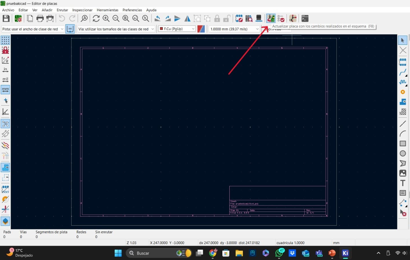
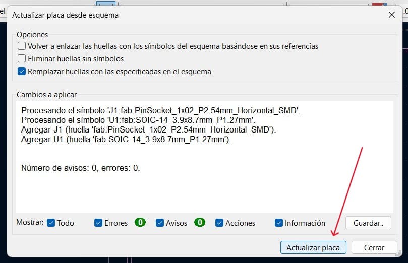
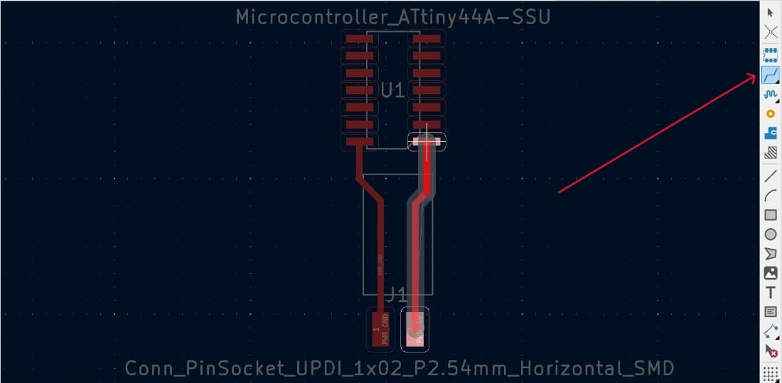
- Update The PCB: On the PCB file we will find an empty space without any of the components or connections we created on the schematic, don't worry, we just need to update the PCB. To update the PCB, we just need to click on the "Update Board" tool and update the changes.
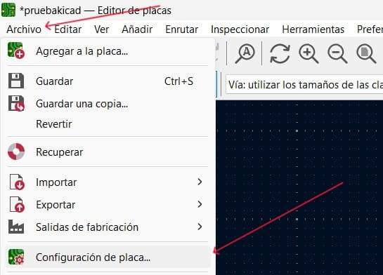
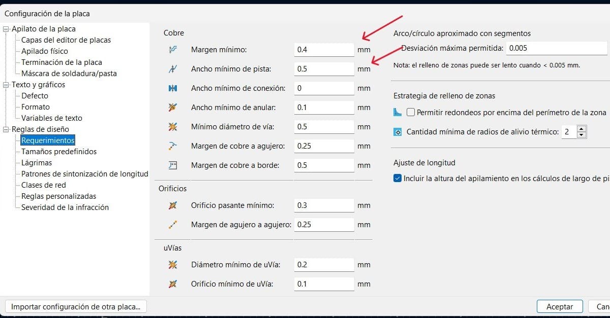
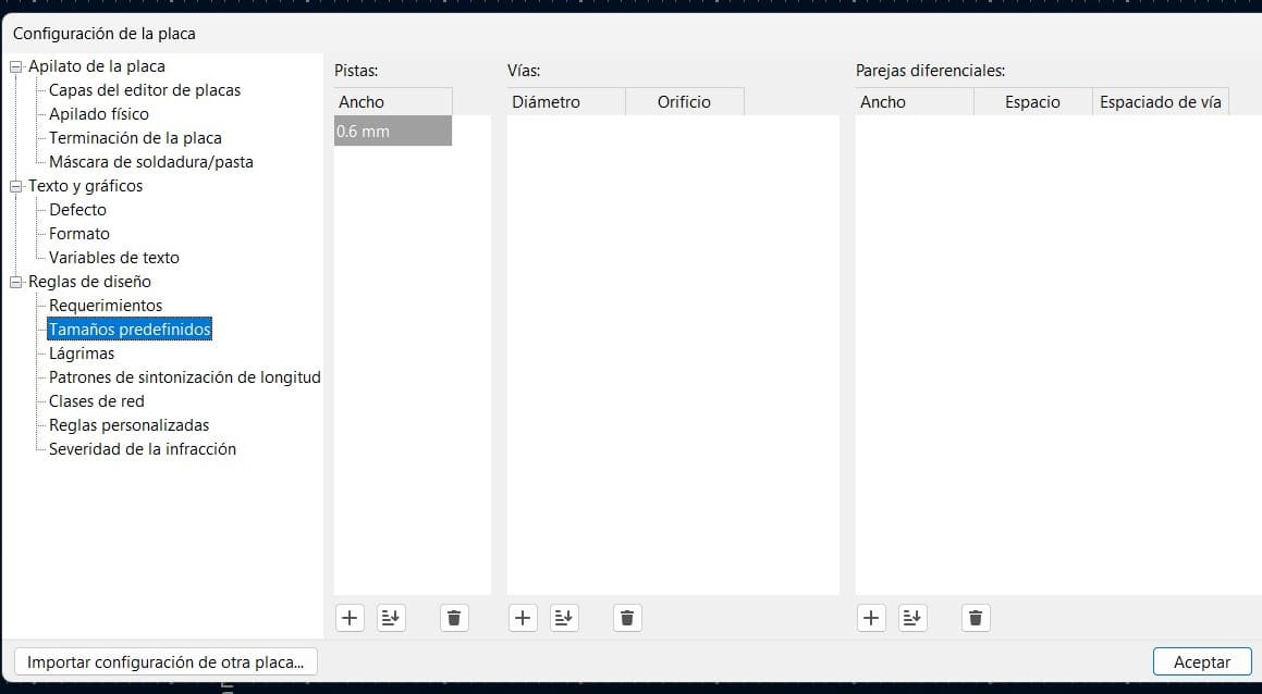
- Design Rules: Before we start making the connections, it is important to defina the rules that our paths need to have. These rules depend on the cutting machine and the tool we are using for the cutting process. In my case, I used the information of the group task website. To set the tolerances, we should go to "File" and "Set Board", once there, we would change "Requirements" and "Default Sizes". In my case, I will use a minimun clearence of 0.4mm (due to the thickness of the tool edge) and an minimun path size of 0.5mm (due to the testings made on the group's website). One of my evaluators recommended me to use paths of 0.6mm (you can change the size on "Default Sizes"), advice that I took.
- Connections: The connections here are quite simple to create. On our workspace thin blue lines will appear, these lines indicate which pins are connected on the schematic. To connect them, we have one tool that will appear the path neccesary to make the connection. When you click a pin while you have the tool selected, you won't be able to make a wrong connection, the software will only show and allow the possible connections to that pin. The connections should have a red color, something that indicates we are on the right layer (F.Cu), this layer is the copper one and is the one that wont be cut by the cutting machine.
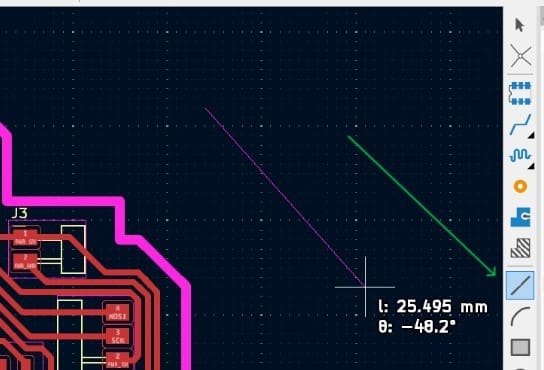
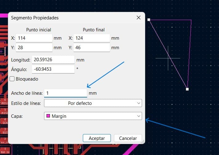
- Margin: After connecting all the pins, it is time to create a margin that will give the shape to the PCB. For this margin, we will need to create the margin lines on the margin layer (the pink one), after finishing the margin shape, I gave the lines a 1mm thickness due to the cutting tool diameter.
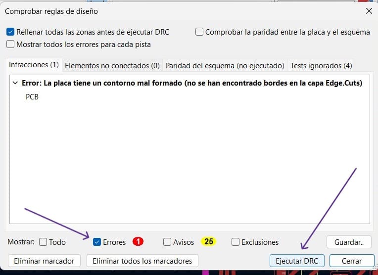
- Checking problems: After finishing the connections and the margin, it is time to check the errrors and warnings. To check these things, you should click on "Inspeccionar" and then on "Comprobar Reglas de Diseño". After running the DRC, we will see the errors and warnings. In my case, I just got one error that was not important, so I ignored it and export my files.
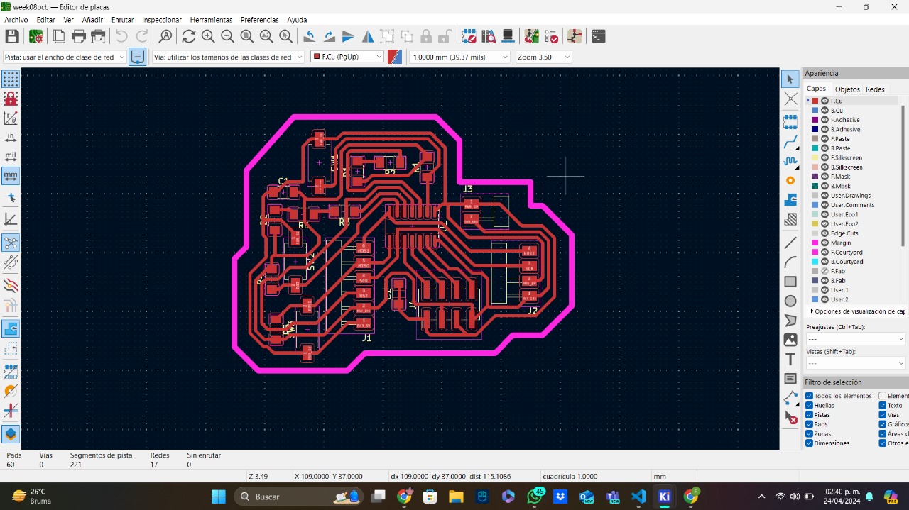
This is a picture of the completed Kicad PCB, showing all the connections and the margin:
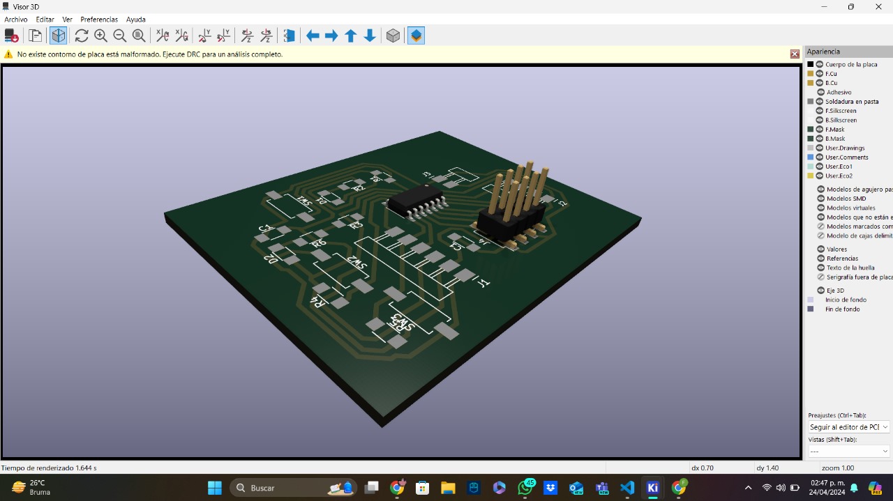
And this is the 3D render of the PCB using Kicad:
Cutting and soldering the PCB
On this section, I will explain the cutting process of the PCB. I won't explain everything because this part has an exclusive week where I explained all the process. You can visit that week here.
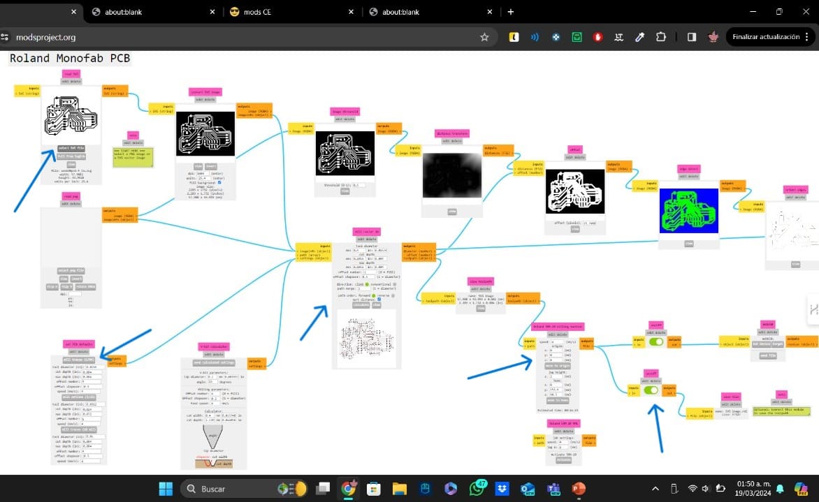
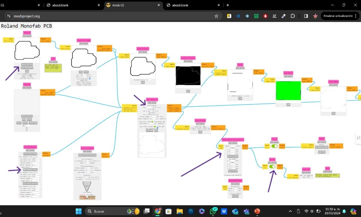
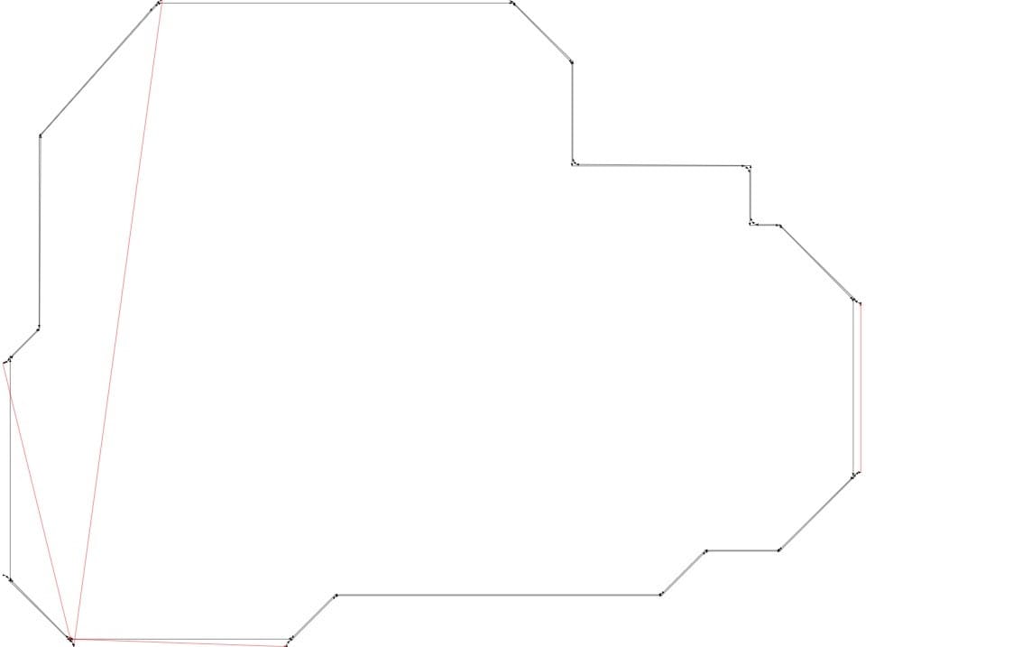
The first thing to do is make the SVG files into cutting files, for this, I used a website called MODS. On this website, I opened two SRM-20 PCB setup programs and I selected my SVG files. For the PCB paths file, I didn't change any of the configuration that you can check on the week 4, but for the margin file, I changed the tool diameter on the main window. The images below, show the settings for each file.
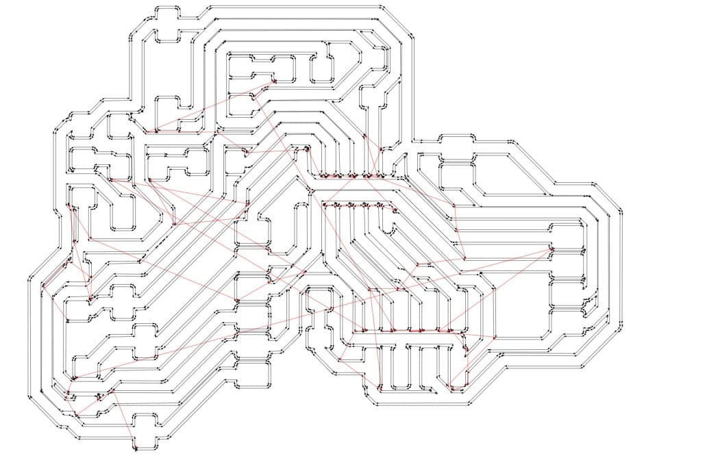
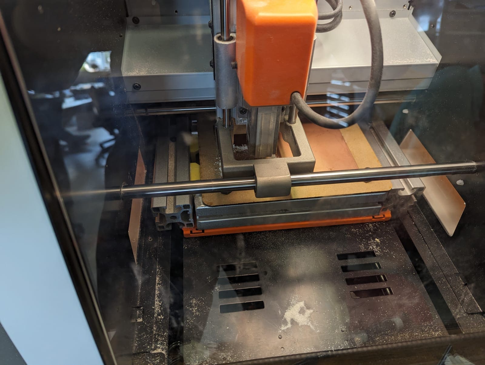
Now, that I am ready with the programs, it is time to use SRM-20 to create de PCB. It is important to remember that the tool origin is on the left bottom corner of the copper plate. After putting the copper plate, I used the Vpanel software for setting the origin and run the programs.
To finish the manual part of this week, it is time to solder all the components. For this week, I used some resistor, 2 LEDs, 3 buttons, the Attiny44, a capacitor and the programming pins. In my case, some paths were joined, so I used a cutter to separate them manually, the separated paths, are the ones pointed with an arrow.
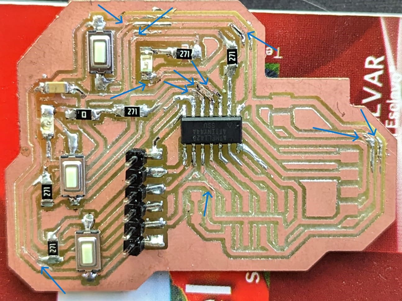
Note: To solder the components, I used a method that consits of applying tin in one of the sides of the component path. After that, I solder one of the sides of the component to the tinned path. Finally, I solder the other side applying the tin on the joint of the component and the path.
Testing
To test my PCB, I made an Arduino code that basically turns on 2 LEDs using 2 different buttons. I used a 3rd button to change both of the LEDs states.
Before programming the Attiny44, we should change the Arduino configuration to the programmer mode. These are the steps to use the Arduino as a programmer:
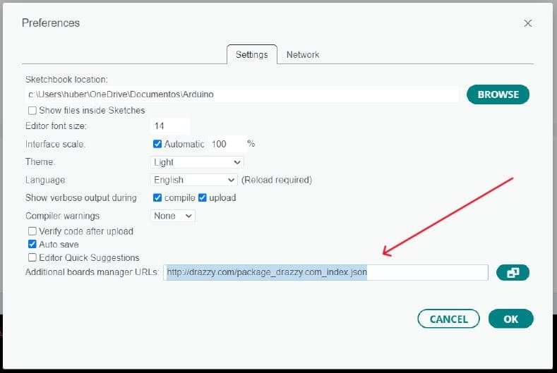
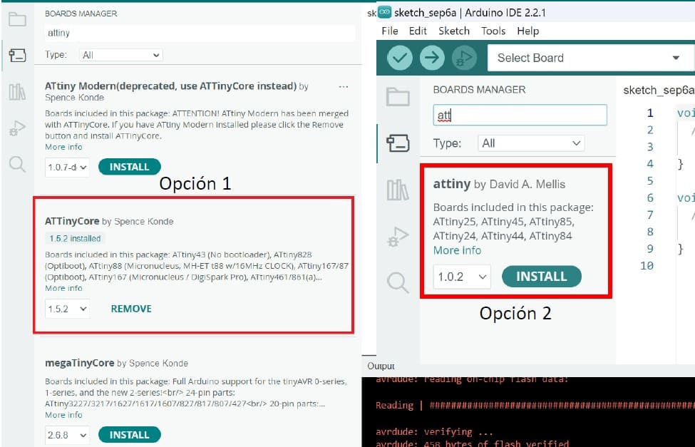
- Attiny Library: First, you should add the Attiny library to your Arduino IDE. To to this, you should go to "File" and "Preferences". Once on "Preferences", you should paste this link: https://drazzy.com/package_drazzy.com_index.json on the "Additional Boards Manager URLs". After that, you should install the Attiny library on the the libraries section.
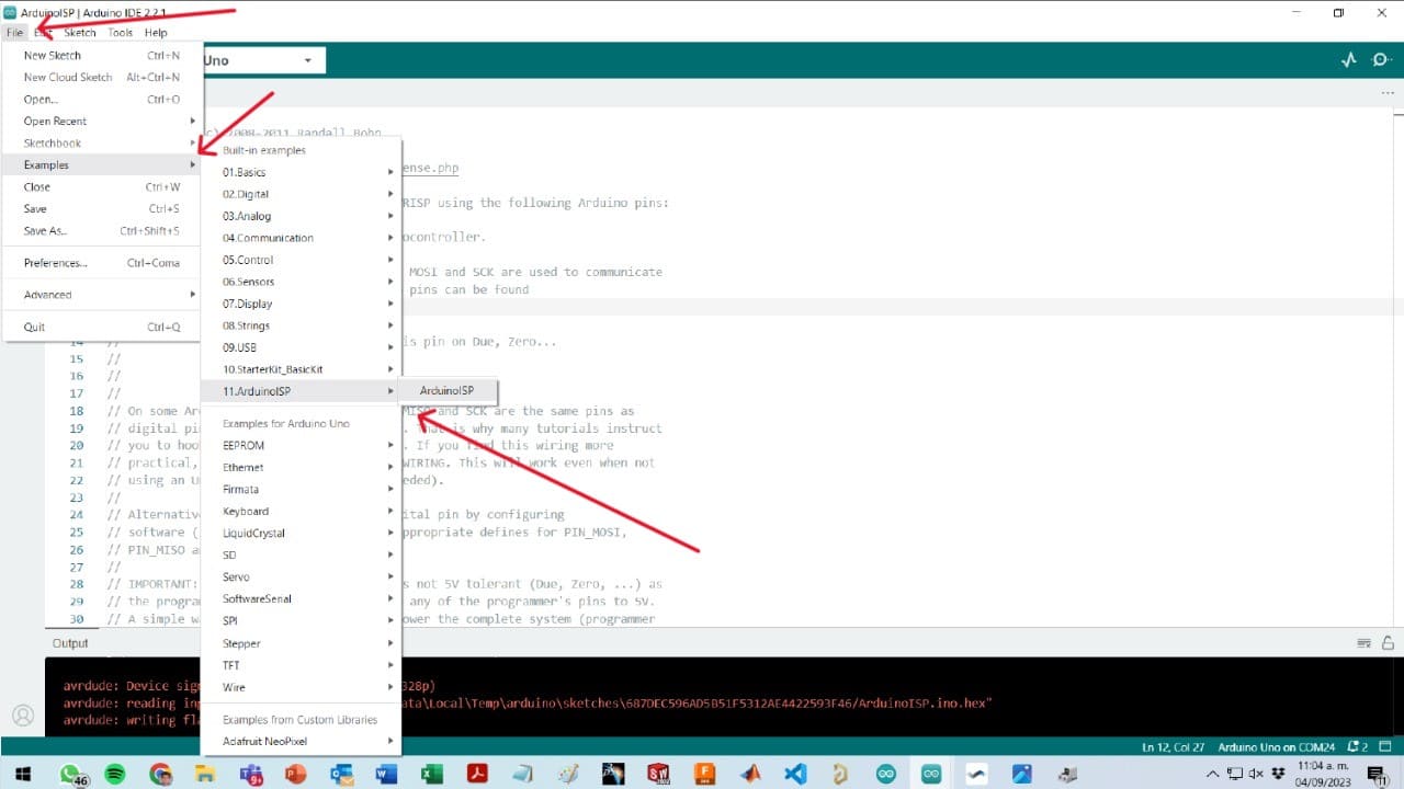
- Arduino as ISP: The next step is to upload the example code "ArduinoISP" to your Arduino UNO. After that, now you will be able to choose the Attiny44 as a board and to use the "Arduino as ISP" programmer, but it won't work until the next step.
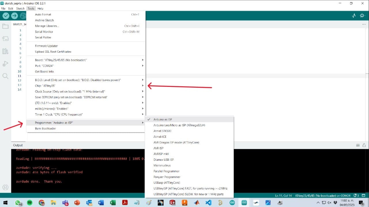
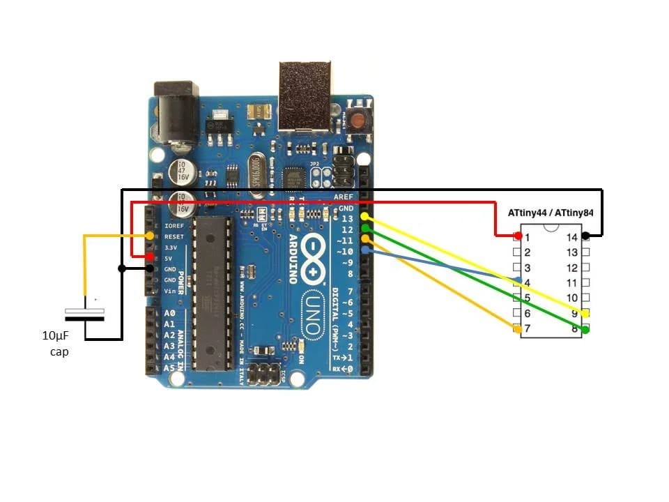
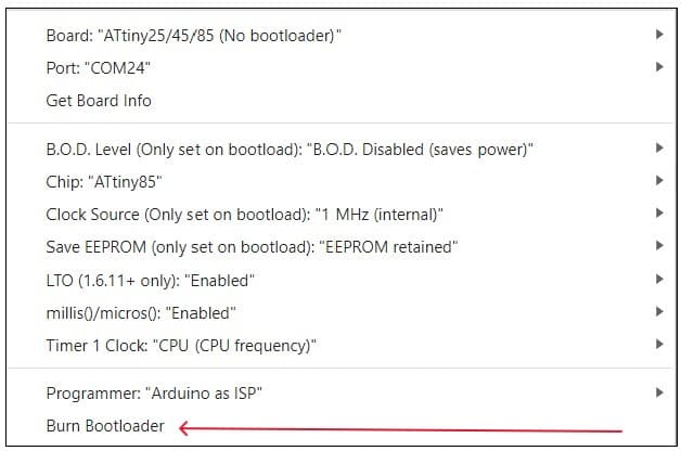
- Burn Bootloader: To make the Attiny44 useful, you should burn the bootloader. To burn it, you should follow the diagram below and the list of settings requiered for the bootloader. After checking and connecting the Attiny44, you should click on "Burn Bootloader".
Now that we can use the Attiny44, it is time to upload the code. The code I used for testing the PCB is going to be explained below:
// Definir los pines para los LEDs
#define ledPin1 9 // LED 1 conectado al pin digital 13
#define ledPin2 8 // LED 2 conectado al pin digital 12

// Definir los pines para los botones
#define buttonPin1 10 // Botón 1 conectado al pin digital 2
#define buttonPin2 7 // Botón 2 conectado al pin digital 3
#define buttonPin3 5 // Botón 3 conectado al pin digital 4
void setup() {
  // Inicializar los pines de los LEDs como salidas
  pinMode(ledPin1, OUTPUT);
  pinMode(ledPin2, OUTPUT);

  // Inicializar los pines de los botones como entradas
  pinMode(buttonPin1, INPUT);
  pinMode(buttonPin2, INPUT);
  pinMode(buttonPin3, INPUT);
}
void loop() {
  // Leer el estado actual de los botones
  int button1 = digitalRead(buttonPin1);
  int button2 = digitalRead(buttonPin2);
  int button3 = digitalRead(buttonPin3);

  // Si el botón 1 es presionado, alternar el estado del LED 1
  if (button1 == HIGH) {
    digitalWrite(ledPin1, HIGH);
    delay(100); // Pequeño retardo para evitar rebotes
  }
  else{
    digitalWrite(ledPin1, LOW);
    delay(100);
  }
...
  }

  // Si el botón 3 es presionado, alternar el estado de ambos LEDs
  if (button3 == HIGH) {
    int ledState1 = digitalRead(ledPin1);
    int ledState2 = digitalRead(ledPin2);
    digitalWrite(ledPin1, !ledState1);
    digitalWrite(ledPin2, !ledState2);
    delay(100); // Pequeño retardo para evitar rebotes
  }
}
Now that everything is ready, this is the video of my PCB working with the testing code:
You can copy the code here:
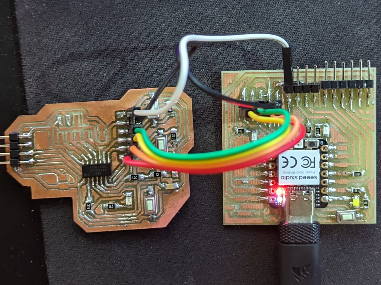
Finally, I tried to use the quentorres XIAO RP2040 used on the week 4 as a programmer. I uploaded the Arduino ISP code and used in the same way as I explained it some minutes ago. I also looked for some tutorials on internet. The most useful tutorial in my opinion was this one. Here is an image of how I connected the RP2040 to my board:
To download the files used for this week, you can click here.