8. Electronics design
EasyEDA
For this week I used the software EasyEDA. This software is free and has a wide variety of tools and a big library, and it's also online, you can download it to get the most of it, but the online version is still really good, you can click here to try it yourself. I used this software because with it I can work from anywhere just with my account, without the need to download anything, but I recomend to download on your own laptop or PC because it doesn't deppend on Wi-Fi as much and it ain't heavy.
PCB
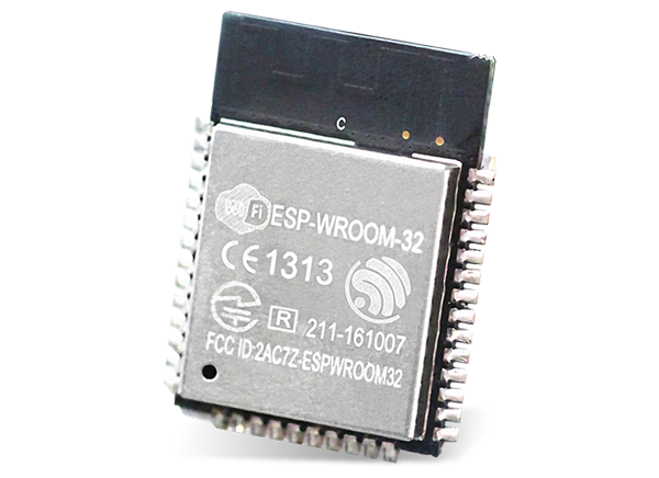
This week I designed a PCB for an ESP32 wroom, this microcontroller is really special because it has WiFi and Bluetooth modules integrated, I want to use it for several functions and one of them includes bluetooth. Check Week 8 Guide Ibero Puebla Fablab for support material.
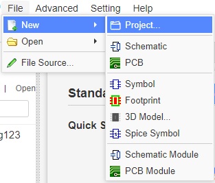
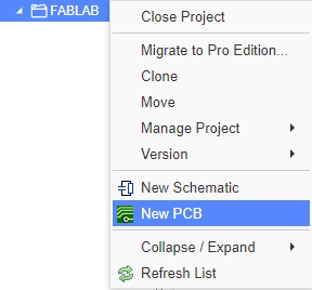
The software I used is EasyEDA, it's very intutive and well easy to use, first you must create a new project, the inside the project you can create either a new schematic or a new PCB, usually go directly for the PCB design, but since the ESP32 has a lot of pins I started with a schematic to help me guide the connections.
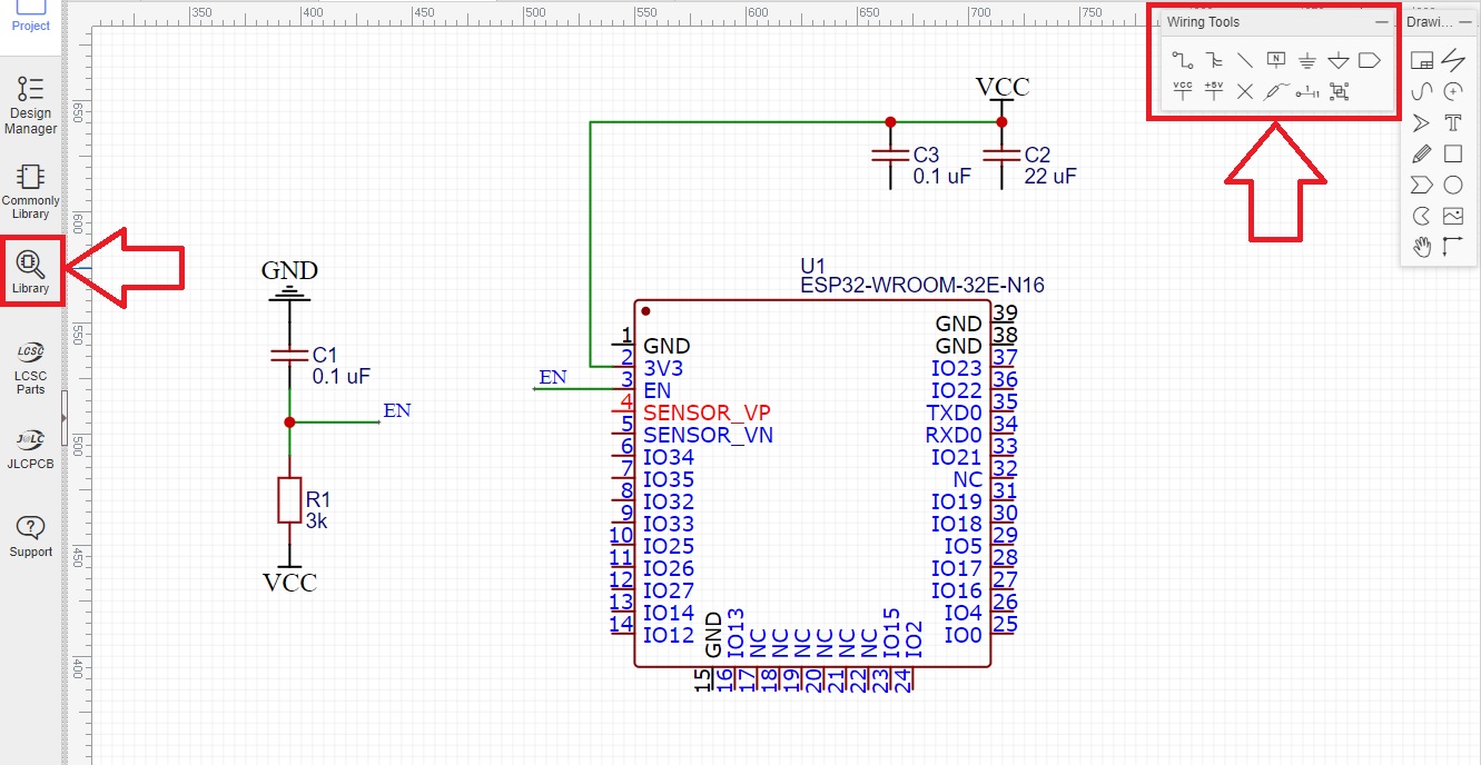
The EasyEDA interface is very intutive, on the left side you will find the library, there you can select the components you want to use for your schematic design, on the right side you will find toolboxes, these are used to create connections between components, refference points for Vcc and GND and name tags, so your schematic is well organized.
When we are done with our schematic we can create a PCB design from the schematic, this is useful because the components and connections are imported, but we can also start a PCB design without schematic.
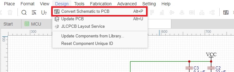
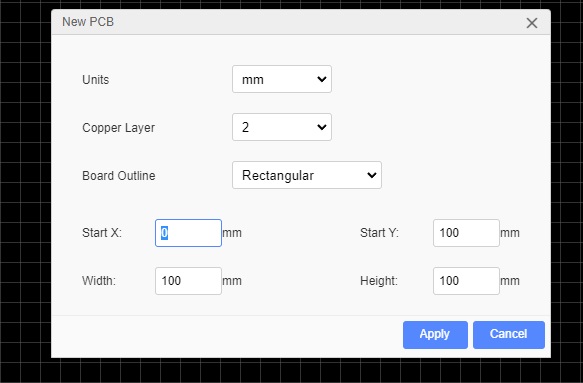
After creating this new file, you will be shown this window where you can select the number of copper layers used, the size of your board and the units that you want to use.
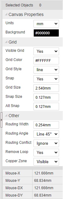
On the main screen you will find this tab on the right side, with this you can change the units, color adjusments for the grid, and the most important: the width of your lines, this is important because dependending on the voltage and current you may need to change the width of the lines.
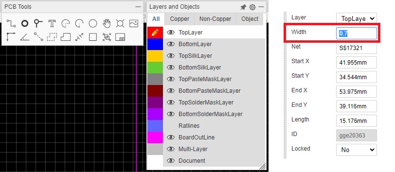
You will also find the PCB tools and layers and objects, on the first one you can draw the connections, holes to drill and many other things. On the second one you will find the color pallets, every color corresponds to a different layer on the board. For our machine since we are using a V-cutter, we need to have our width set to 0.7 mm so the lines are validated in the settings of our machine, for the purple lines that correspond to the board outline we need a width of 1.0 mm.
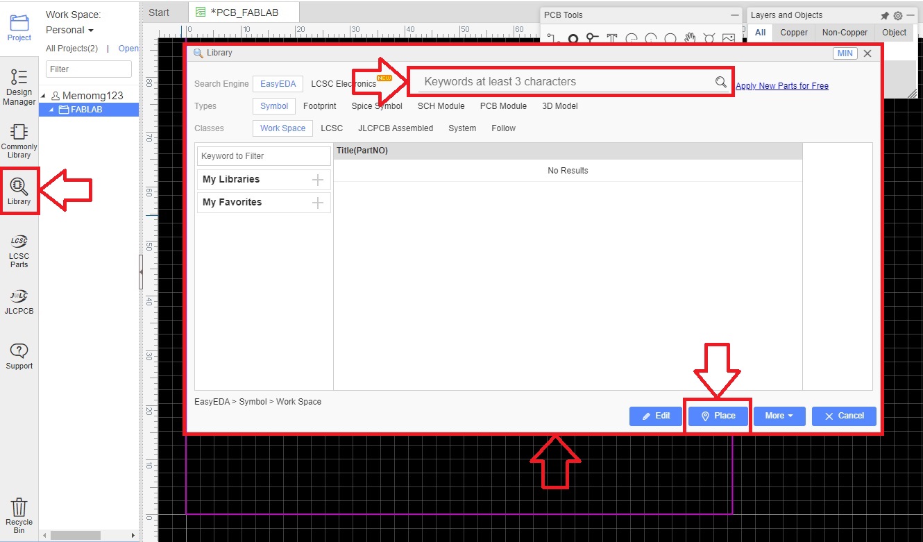
And the most interesting part is the component library, on your left you will see a menu there click on "Library", just like with the schematic, then you will see this window where you can type the component you will be using and it will be shown, click on place to put the component anywhere you want in your design.
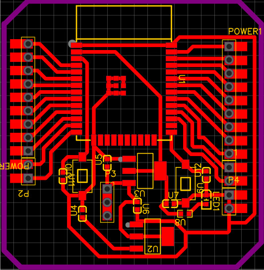
After a while of doing this design I ended up with this:
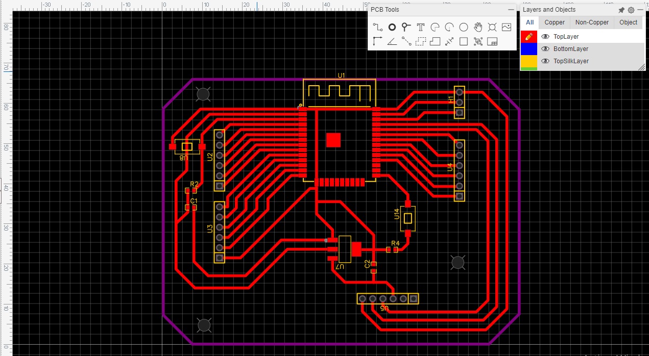
I didn't love the design so I worked around it, changed some components and reduced the size. I swapped the enable push button for a resistor, it works basically the same.
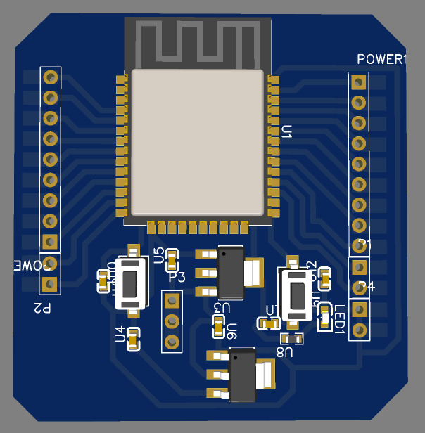
Simple and functional, then I fabricated it with our Roland milling machine, check my week 4 page for a more in-depth introduction on how to fabricate a PCB. But first, we need to export the parts we need for the program.
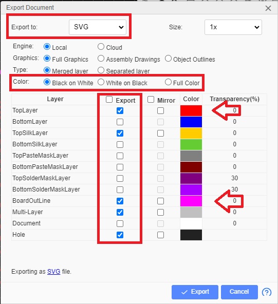
First on the toolbox look for File and click it, then on Export, and select the type of file you want, I recomend .SVG over .PNG because it has higher resolution.
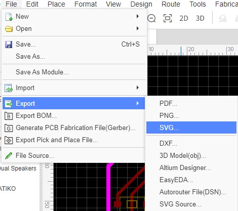
Then this window will appear, we can check what type of file our design will be exported to, the colors (for mods we use black on white for outline and white on black for traces), and also the color palette of the layers and objects, this is very important, because we need to select which will be exported, as we are only using the top layer (red) we need to export that one on a different file to the outline (purple).
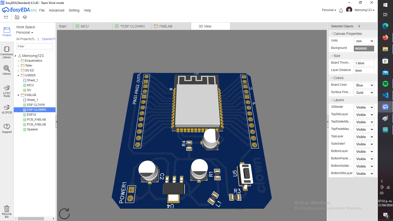
Something I really like about EasyEDA is the 3d models you can create from your PCB designs, just like this one, you can check the parts that you are using, the size of the board and how it should look like after manufacturing it.
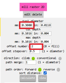
Since the ESP32 has some very thin connections, on the MODS website we need to modify some parameters so the traces come out correctly, they are as followed:
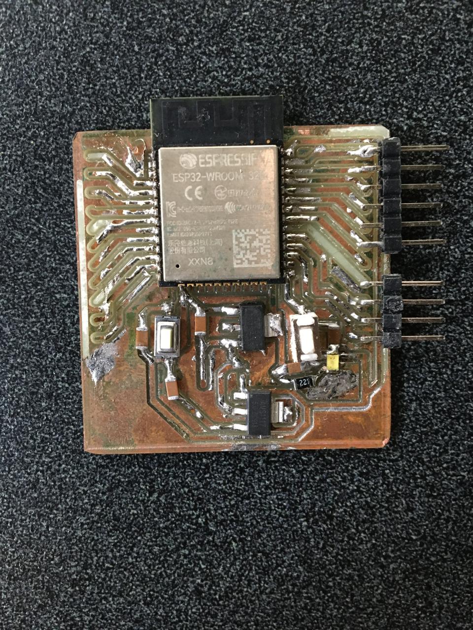
After soldering the necessary components, here is the final result:
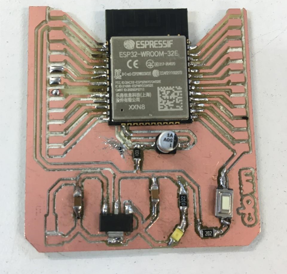
The bed of the mini mill was not well calibrated so part of the board at the top got chopped off other than that it works really nice.
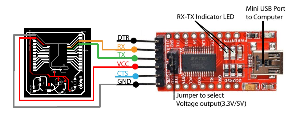
To program it, we need to use the UART communication protocol, you will also need an RTDI, this is how the connections should be made, when we use RX/TX we must invert them so one boards RX goes to the other TX.
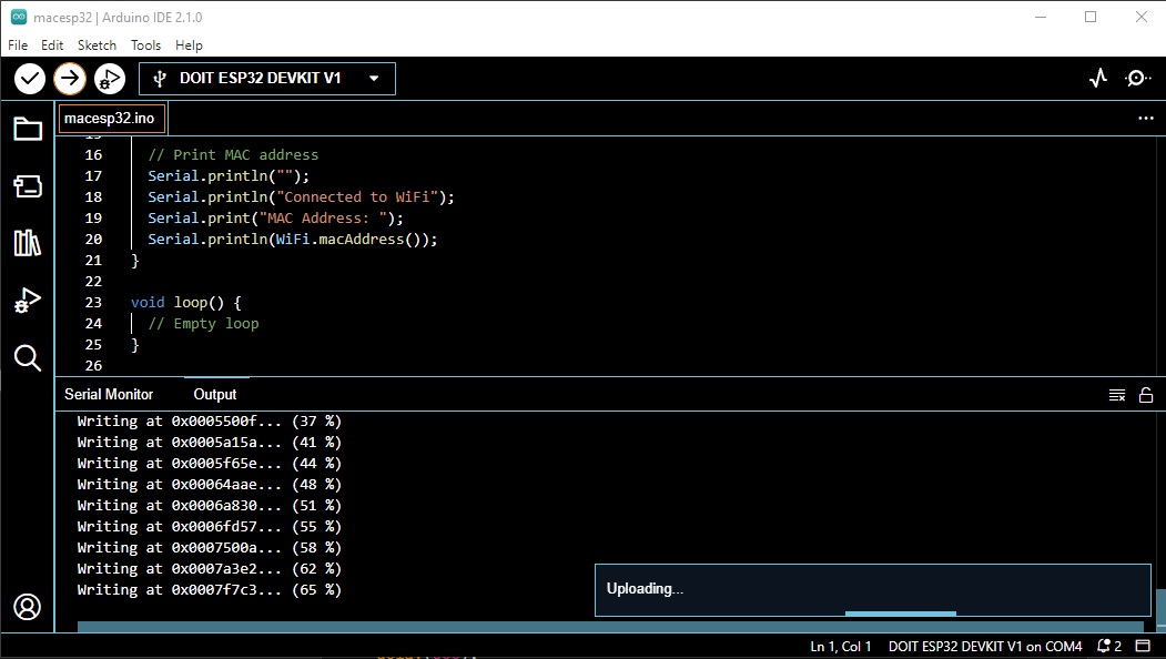
I uploaded a code that prints on the serial monitor the MAC adress of the ESP32.
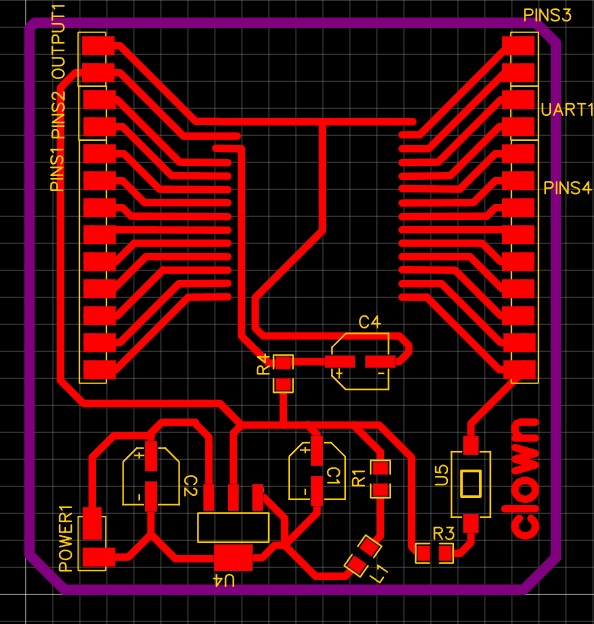
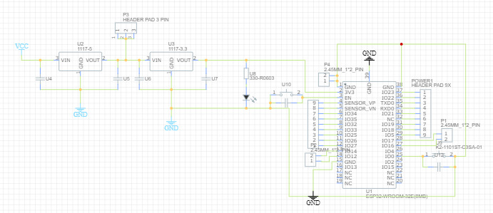
As you can see it has some problems, first of all the enable is connected to a capacitor instead of the traditional push button, and the part at the top broke, when I tried to program something else it failed so I decided to make another PCB design, this one with the enable as how it normally connected, this is the PCB I made.
You can click here to download it. In the end I used a different ESP32 part than on the previous one because this footprint allowed me to edit the pins on the back.
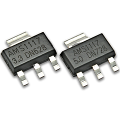
This schematic also includes a 5 V regulator, this are the materials needed:
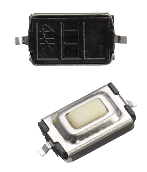
| 10k resistors | 1 uF (2) and 10 uF (2) capacitors | AMS1117 3.3 and 5 V regulator | Push buttons (2) | Male pinheaders |
 |
 |
 |
 |
 |
After creating the PCB design I tried to follow the same route to make it slim. You can click here to download the traces and here to download the outline. This is what it looked like:
You can click here to download it. Here's the 3d model for it:
I did put it together but after some testing I believe the ESP32 got burned out.
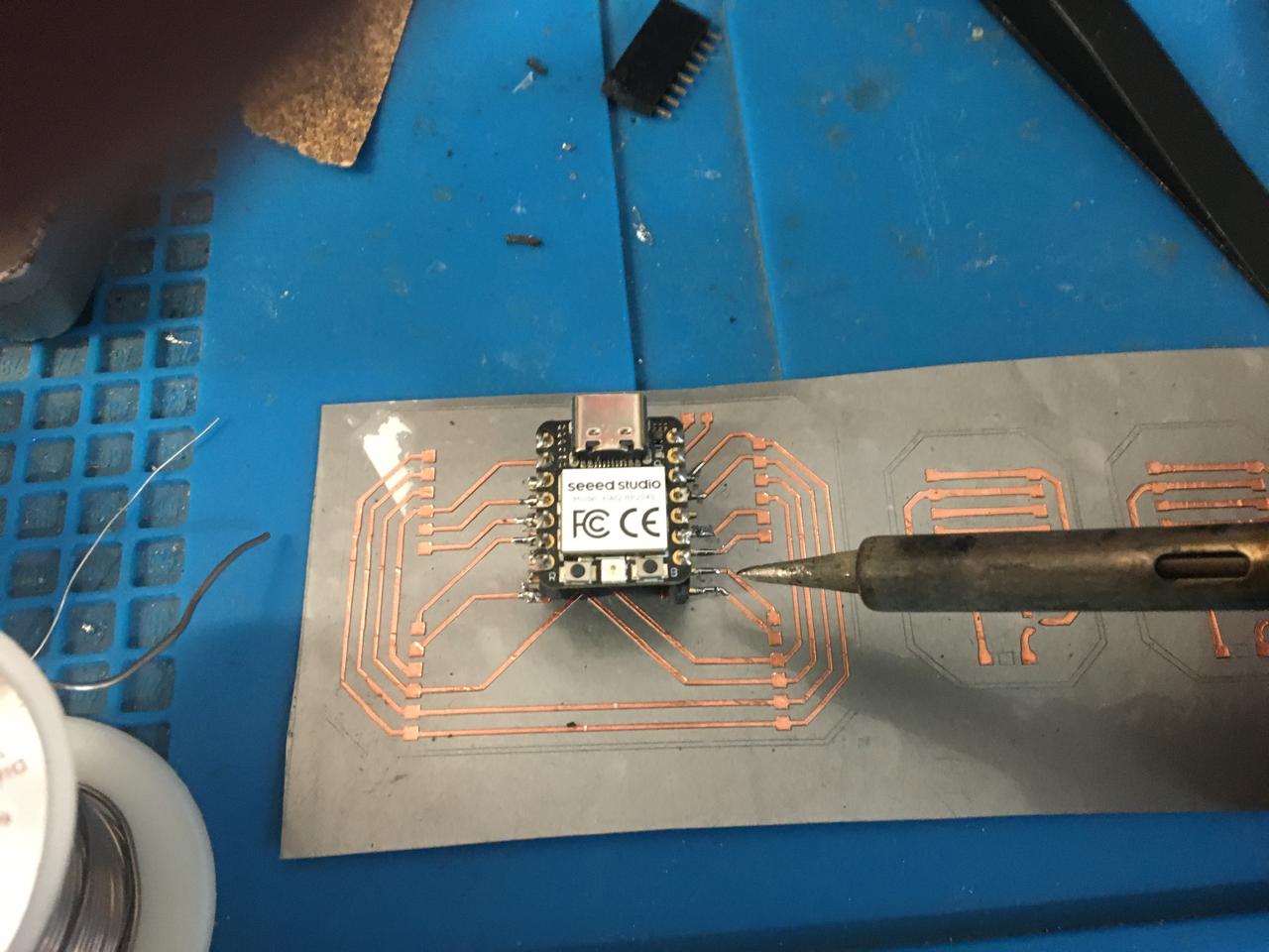
FCB
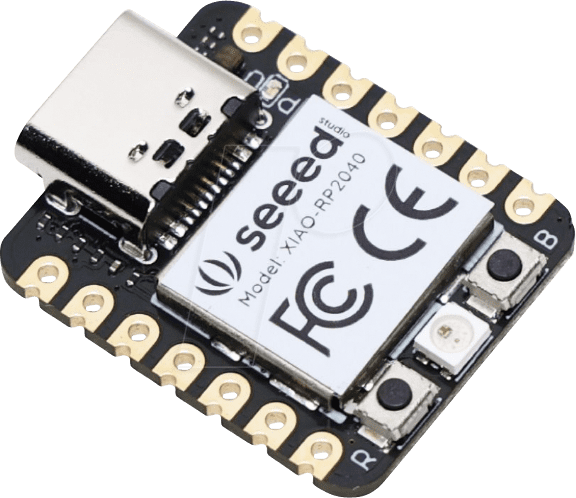
I also made a flexible circuit board for a XIAO RP2040, you can download it by clicking here.
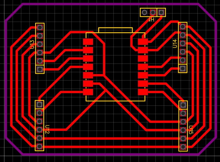
This circuit will be used on my inputs week, it was really fun to make so let's get to it. First, I made this design, since this board will be used with four sensors with the I2C protocol, I needed 8 I/Os pins, 4 SDA and 4 SCL pins and of course GND and 5V.
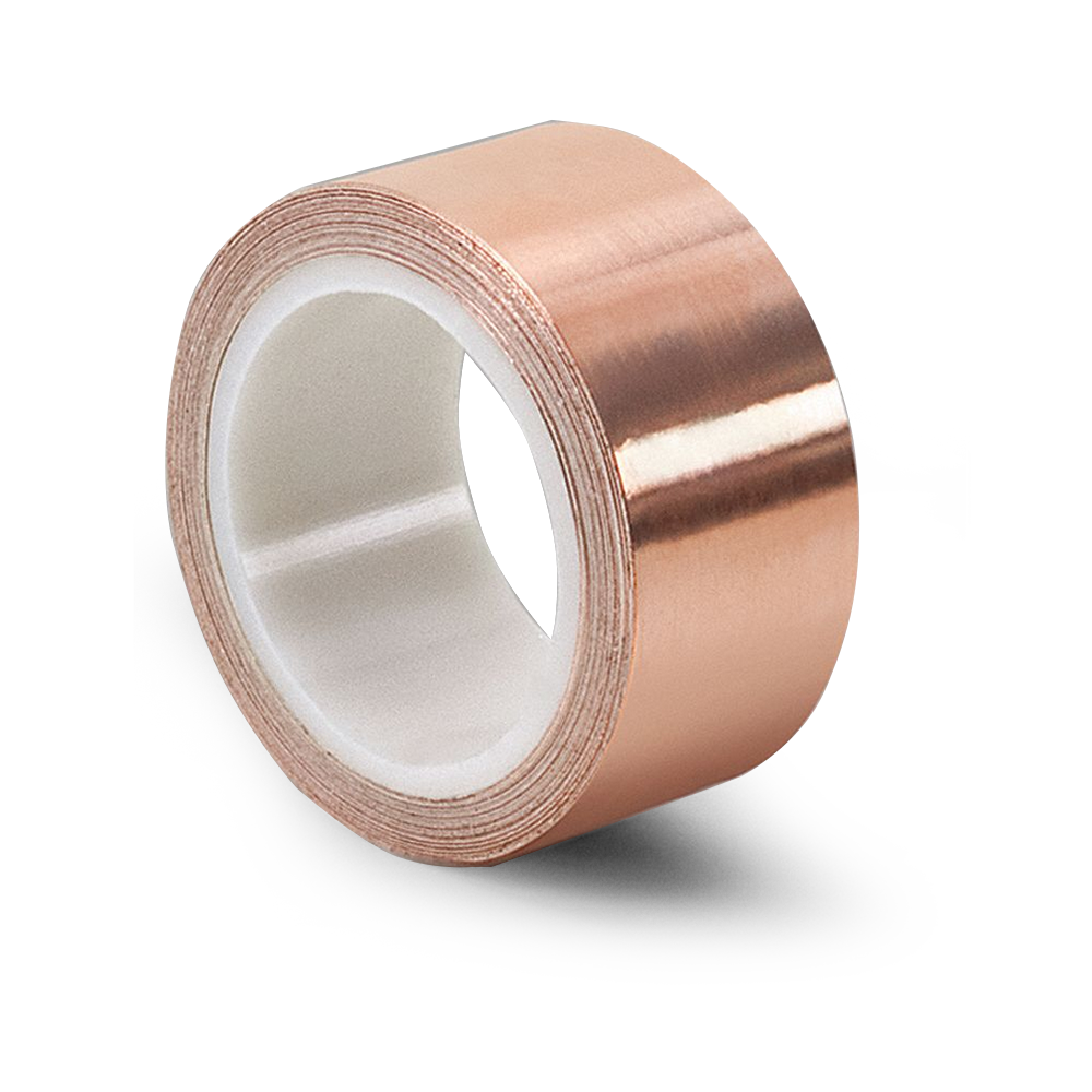
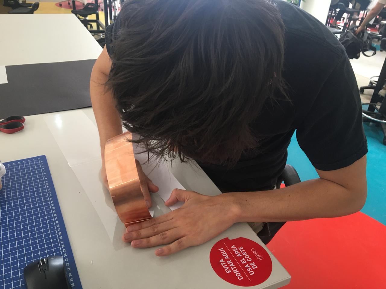
To create this type of circuits we need a copper tape, acetate and a vinyl cutter.
First, we paste the width of our acetate sheet with copper tape.
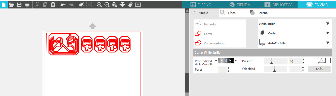
Then, we load the acetate onto the winyl cutter, for a more indepth guide on how to cut with this machine you can check my week 3 page we can use the same parameters to cut bright vinyl.
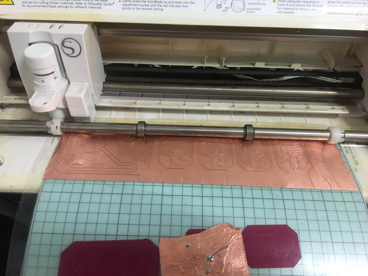
After the cutting is done we just need to peel off the excess copper, this process is a little tedious, so if you try it yourself graba cup of coffee and a pair of antistatic pliers.
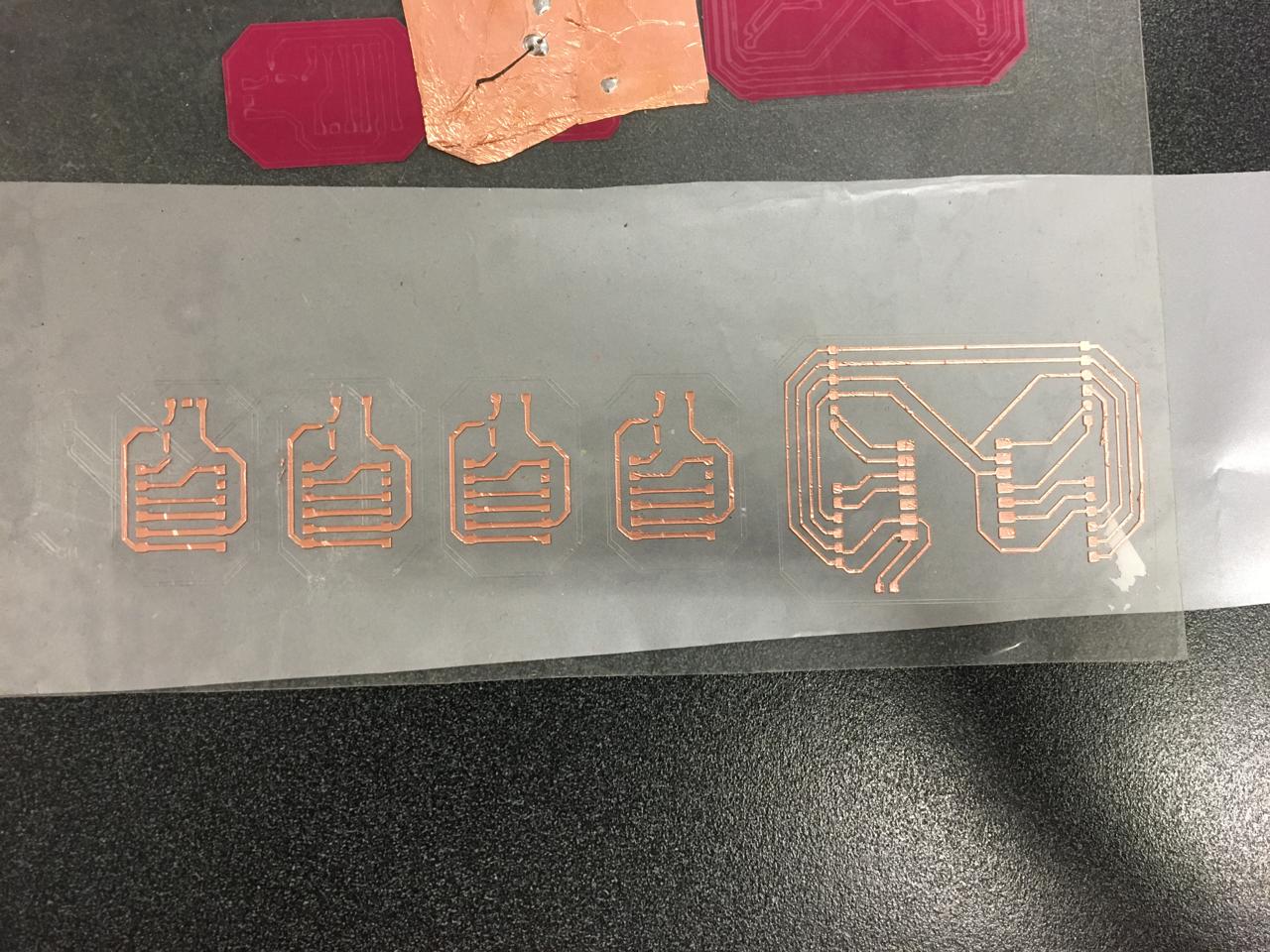
After peeling off the excess here is what your fcb should look like, I also pasted vynil on the back for decoration and hoping it would work as bit of thermal support for the soldering process.
Finally I just soldered some female pinheaders to plug a XIAO
I learned a lot and experiment a lot on this week, the flexible circuit process is great and I plan to use it again.