8. Electronics design
This week's practice consisted in making our own PCB design, testing the electronic design rules and
making it following the same process from
Week 4 . As we had to understand the elements around electronics, this was pretty
intensive for newbies like me, but I got a lot of knowledge from it.
Also, during this week we tested useful equipment that might be found at our Fab. The information is
available at our group site and you may access by clicking
Here .
What did I learn from electronics design?
Mostly terms and concepts related to circuits, also considerations to build tracks, what to link, where and why. As the main concepts, here are some of the basics I got:
| Concept | Description | Picture/ Symbol |
|---|---|---|
| Voltage | Strenght with which electricity flows. |  |
| Current | Electricity flow amount. | 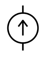 |
| Power | Rate at which energy is transferred or converted. |  |
| Ground | It's a reference point in an electrical circuit that serves as a common return path for electric current. |  |
| Resistor | Component to resist voltage and avoid short circuits. The ones you use depend on your other component's requirements.They don't have voltage, nor current limit, their limit is on power. | 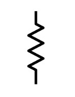 |
| Capacitor | It's useful to store energy in an electric field. These are polar and not always required for a circuit. |  |
| LED's | They are polar, when soldering them guide with the green line they have to place them. This line is the cathode (negative ) side. |  |
Microcontroller | The brain of a circuit, It allows to design names to the pins and program them later. It's possible to connect them directly if they have ports of communication, if not they can use another one. | 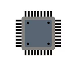 |
Footprint | It's the physical layout or pattern of a component's pads, holes, and other features on the PCB. | 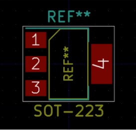 |
Schematic design | It's a graphical representation of an electronic circuit. It illustrates the connections between various electronic components using their symbols. | 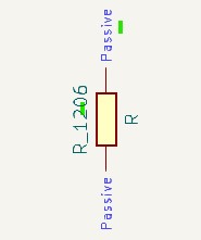 |
During the development of this practice I got to understand some rules that might be obvious for people with enough experience, but I will list them here as personal notes:
- When you make the traces, they must have one side linked to the ground and one to voltage, the circuit must close at some point.
- Try to have a resistor per component, some modules already include them.
- All of the traces with the same function must be connected to close the circuit. Eg: All of your grounds and Voltages, In case you have more than a single pin for it in your microcontroller.
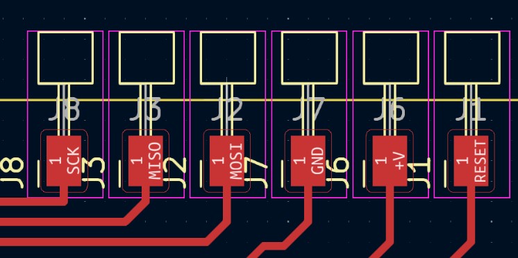
- Consider to always include some important pins to program your board later: MISO, MOSI, SCK, GROUND, VOLTAGE and RESET.
- Export the files for cutting the PCB from different layers of the same version of a file. Don't add the outline frame from a different file because the measurements may change.
Adding libraries to KiCad
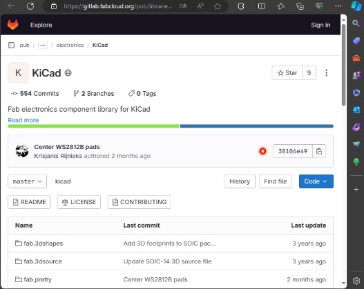
As the libraries you add while working with arduino, it is also necessary to add them when you use KiCad, so the first thing we did this week was to install the one that had all the component my FAB has.
- First we received a link to download the component library for all we have in the FAB
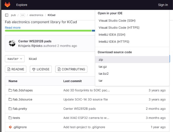
- I downloaded the floder in a ZIP folder, as if I were cloning the repository to
my
computer.Then I decompressed it to check the files in a location I could easily find.
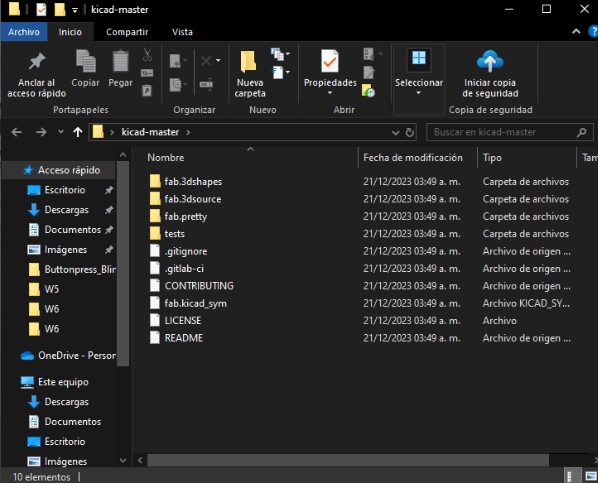
- Next, I opened KiCad and uploaded the first folder from the preferences
tool.This was to get the schematic.
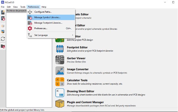
- This already has default libraries, so I had to import mine from the + buton.
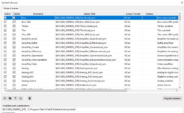
- Then I looked for the file fab.KiCad.sym to add the symbols, I saved it with
the
name "fab" in lower case.

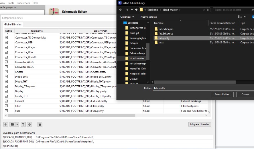
- Now I did the same to add the footprint>.

- There I added the folder named fab pretty. To name this library, i called it
Fab with the first being capital, to avoid confusions later.
- Finally, I imported another folder called KiCad to the configure
pathsThen,
it was all ready to start designing.

Making my own design: The first schematic
- First I didn't have much idea on what to do, the only thing I was sure about was
that I really wanted to make my own game controller.
I looked around for some references of other DIY pcb controllers.
Click here for the main references.

- I also checked some references on the site recommended last sesion called flux ai. It allowed me to review a board, it's components and layers, from the schematic to the PCB itself. For my practice the biggest reference here is this. The site is available if you click, here .
- After checking both reference I realized they made their boards with two layers, so my challenge would be to make my own at one without mixing traces.
- I started to design by creating a new project on KiCad. Immediately when you
create one, you must select the folder where you want the files to be.

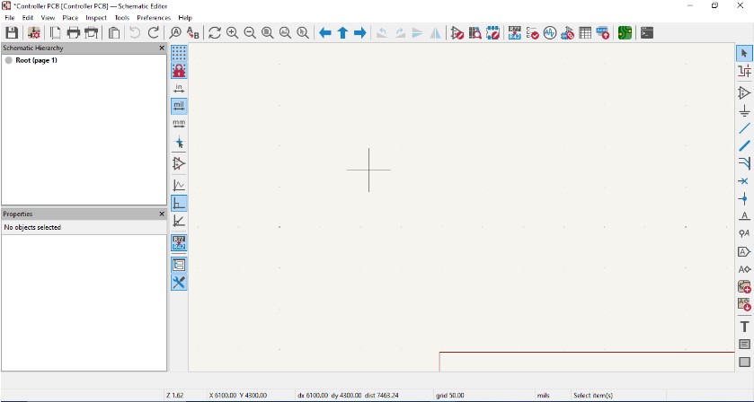
- Then I selected the Schematic editor, that would allow me to arrange the
components and make the connections between them.
- When it opens it looks like this. It has the options to add and modify
symbols.
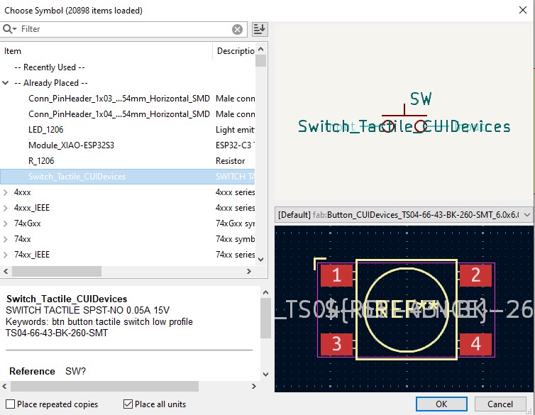
- Then I used the Add Symbols option to look for the component I needed, I
started looking for buttons.
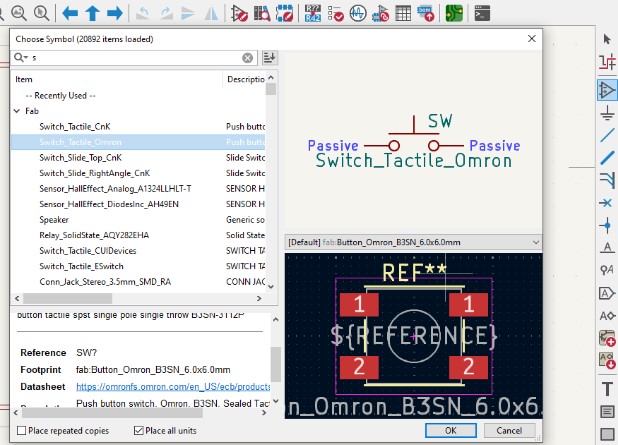
- As I didn't know if that was the one I wanted, I clicked on the datasheet link
,
so it could open a PDF on my browser and offer me a picture. These were the
ones, so I added 4 of them.

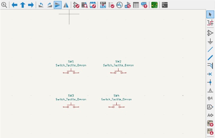
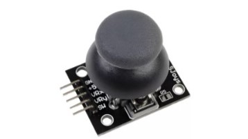
- Then I looked for the pins here, because I needed two of them. As these are analog
components, I Checked the amount the joystick module has, so I added two
with 5 of
them.
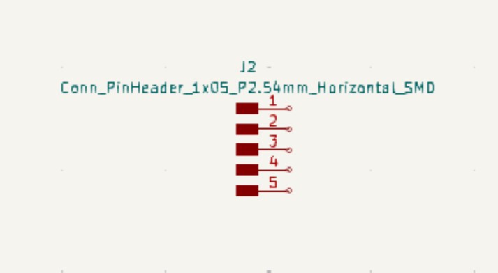
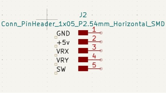
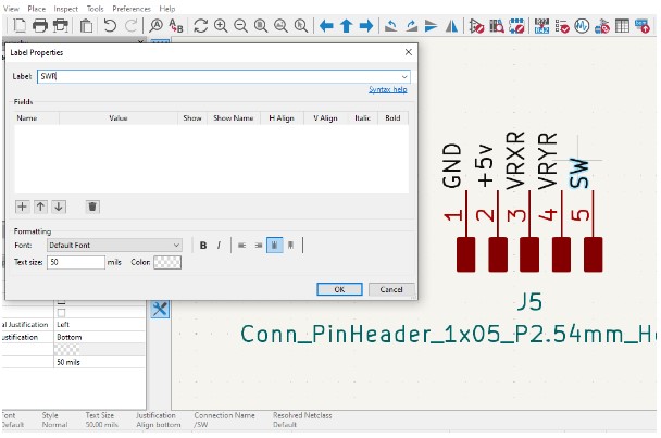
- Then I assigned them a name using the Draw netlabels tool. I gave them the
same names as the ones on the module.
- Then I added a resistor to each button, and placed them on the upper right corner
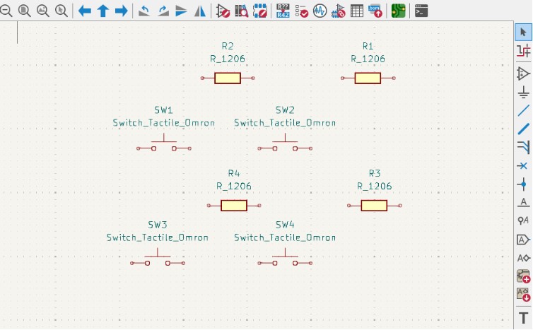
- Later, I added the voltage symbols to the edge of the buttons . So I would know the right side.
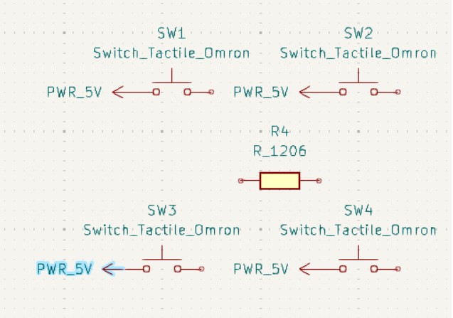
- As I already had a side of the circuits "connected", I added the symbol of ground next to the resistors, so that it would be connected on the other side.

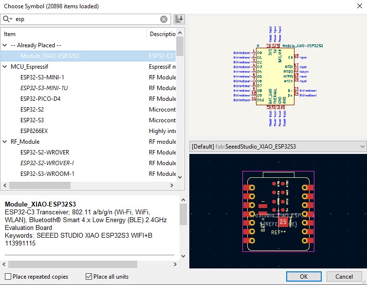
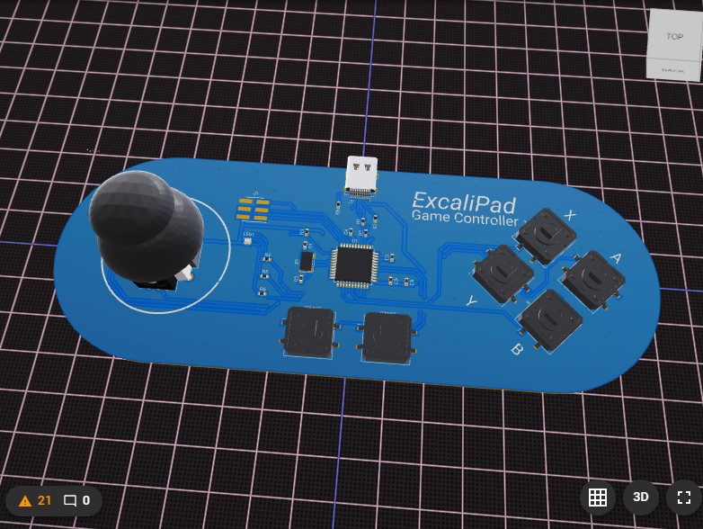
- At first I added a Xiao ESP32C3 as a microcontroller, hoping to take advantage of the pins and usb C already attached, so this is how the schematic looked like before starting to edit it on the PCB option.

Making my own design: The KiCad PCB edit
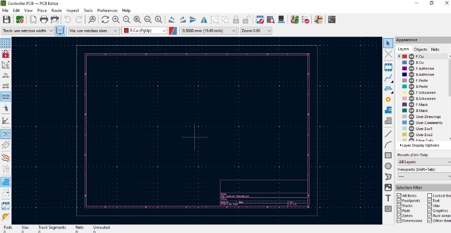
- To edit the pcb I opened from the menu that appears with the folder of the
project, you have one default, so I only had to click it to open.

- This is how it looks when you open it, it doesn't show any preview of what you
do on the schematic.
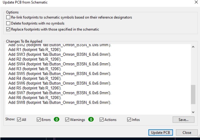
- To update the current design, I clicked on the tools option, and then
on the update from schematic option. There appears a message showing
which pieces will modify. Everytime you make a change on the schematic, you must
update it again to verify everything works.

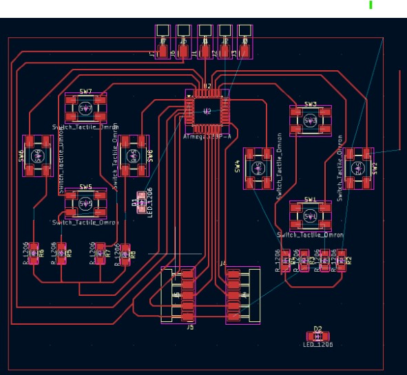
- After updating, It showed me the pieces all together, The blue lines are the preserved links between components I had from the schematic. Note: If something is not linked visually by a blue line here, it won't allow you to join the components with trcks.
- The next step here was to separate them and try to accomodate them to the right place. This way I had a preview of the size and distribution before making connections.

Making my own design: Going back and forth between the schematic and the PCB editor.
- To guide me during the wiring and connecting, I drew these lines to help me know what to conect and where.There I realized maybe the pins from the Xiao ESP32C3 were not enough, so I wired on the schematic and also tried the same with another microcontroller.

- As I wasn't convinced about the microcontroller, I changed itagain and started connecting from the pcb editor. This time it was another version of the Atmega328 on a square format. This ended up becoming the final microcontroller choice.

- Once I started to connect, I realized I would depend on an external module to program this microcontroller, so I added the pins to program/ connect it later. Also, I remembered that I can use tags instead og directly connecting it from the schematic editor.
- I started to wire following the design rules, so as my Atmega328 had small pins, the traces were also very small and I had to be careful and patient.

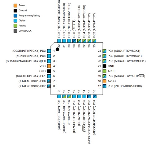
- To know where to connect what, I based on the datasheet from the microcontroller, it was much easier also to add tags on the schematic. This type of image it's available for every microcontroller and you find it as "pinout"
- Also, I realized the joystick pins had the same names. To aviod confusion or mistakes, i renamed them based on the side they would belong to, using a letter standing for it.
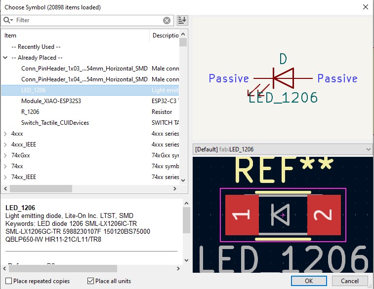
- As I asked for some advice, what I wanted was too much for a beginner and I would put much pressure if I wanted it to work as a finished market joystick. So, I just added two leds to indicate the status depending on the buttons pressed or movements as the output for this week.

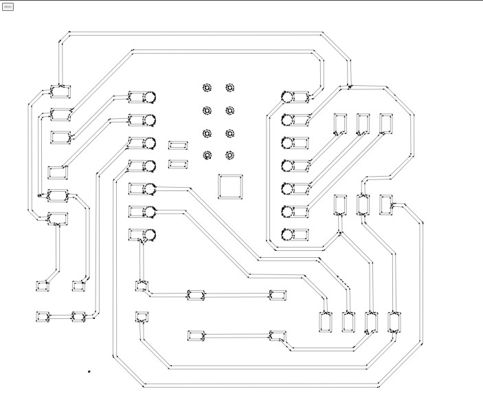
- I also included the respective ressistances and finished making the base traces.When It seemed ready, I drew the frame for it.
- I used the tool inspect design rules to check if the electric connections were correct. Fortunately, the mistakes I had were related to unconnected pins I didn't use.

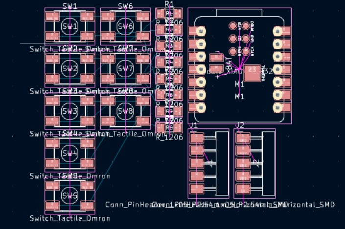
- Also, When my footprint was ready, I drew some rectangles the size of my joystick module, so it wouldn't hit anything, I also drew the frame.
- When I thought I was done, I added another pin to program, so i had 6 in total. I accomodated them based on the easier way to wire.
- Before exporting, I asked for some assesment again, so I noticed my connections were not working becayse my buttons were not connected to voltage , neither the grounds were connected, so I had to wire everything and check again.
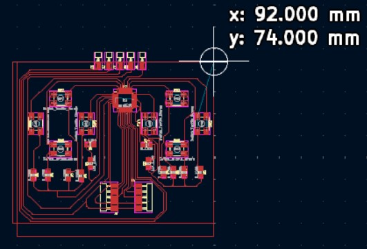
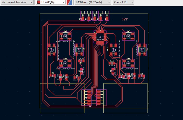
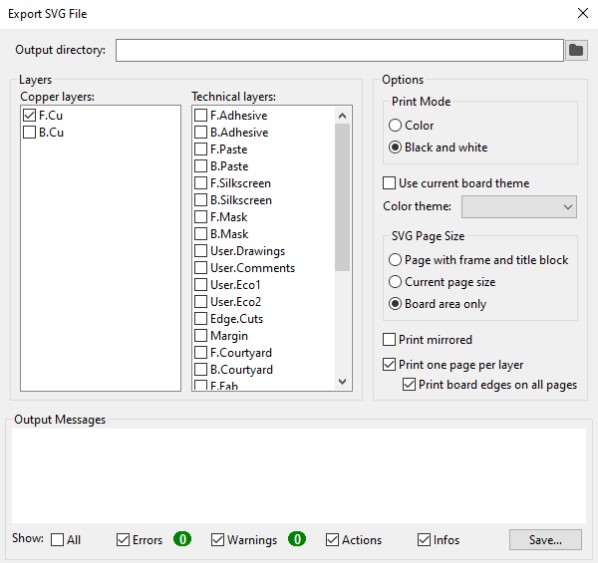
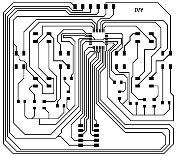
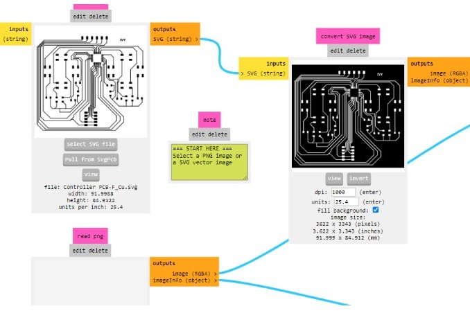
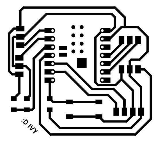
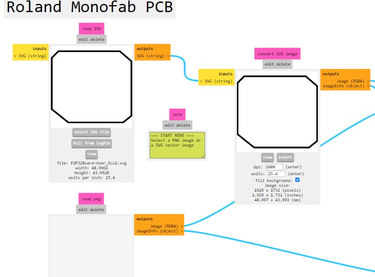
- Finally, I could export the layer with the traces and the one with the cutting frame.The main file is on a SVG format.
- This is how it looked like when I exported the files.
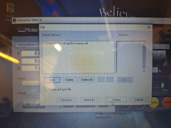
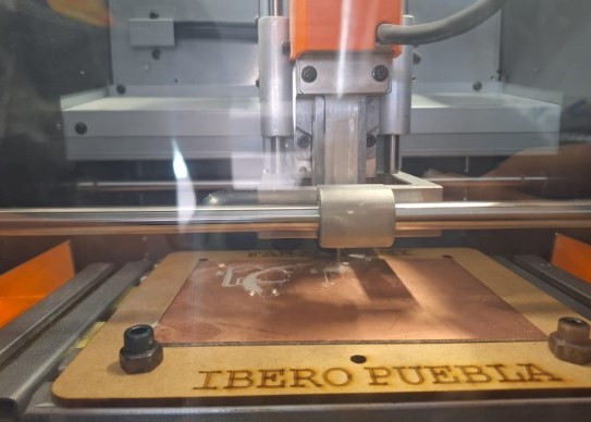
Processing and cut
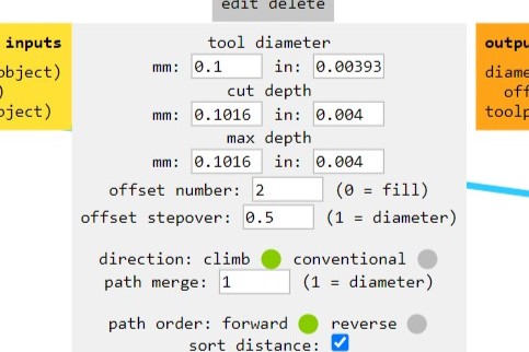
- Once I had the SVG files, I used
MODS To set it all for the cut.

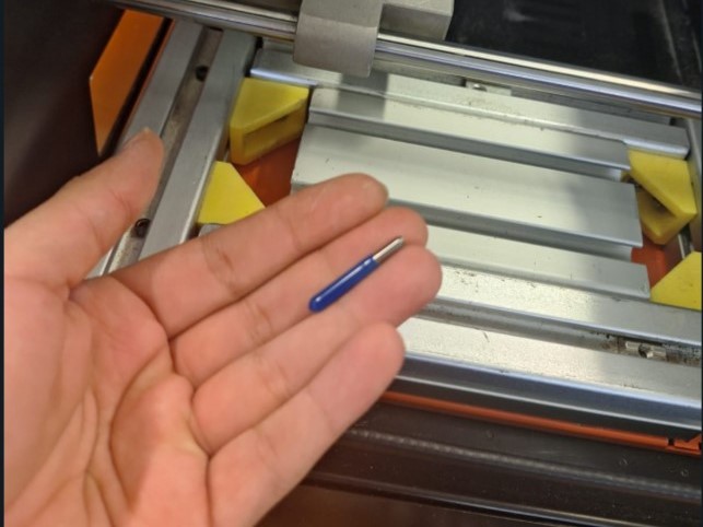
- I used the parameters of 1/64 for the traces and 1/32 for the cut. Also, as my microcontroller was very small I gave the tool a very thin diameter.
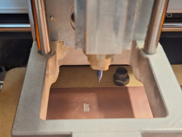
- For my fisrt cut, I used a new V blade and tried to cut over the surface, I also used the remaining parts of my first PCB copper sheet, so I really tried to fit this one. I had the trouble that when the cut started, the spindle worked perfectly, but after some passes it wouldn't contact the surface. I tried more than how I should, because it ended up eating some traces, so I couldn't continue on the same layer.
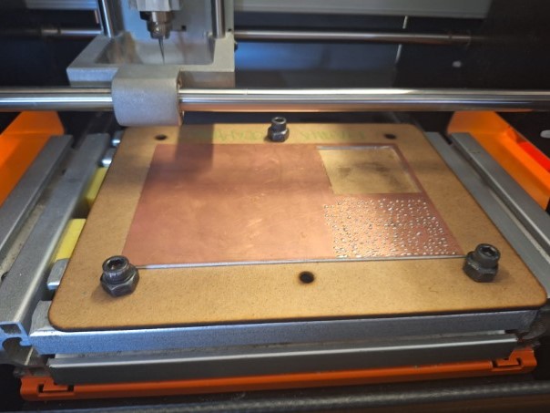
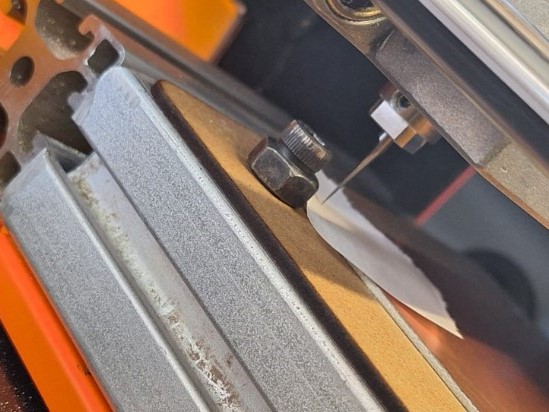
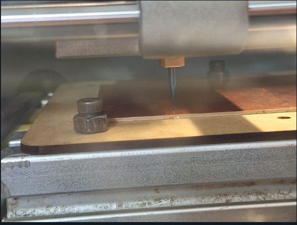
- During my second and third cut, I had the opposite problem. I couldn't calibrate the z axis correctly, because this time the spindle passed just fine and then it would lower itself deeper than the origin. I was still not sure if this was because of the MODS settings or the calibration only, but I will figure out. (At some point I ran out of space). I tried also making a single offset, but I believe the problem relates more with the depth of the cut.

- Take a look at the cut here, and the sound, it was way too deep.
Anti-hero shots (To be continued)
Anti-Hero shots 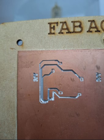
Description for Image 1
Understanding what's wrong
- After reviewing what could be failing, I decided to make think differently, from the calibration to the cutting mill, the bed and the machine itself to the MODS settings.
- I had to run some tests on how to calibrate the bed, because I made
other attempts where I reduced the depth of the engraving and it seemed
to work, but when It finished, the cut was mostly superficial or at some
point the tool didn't make actual contact with the copper.
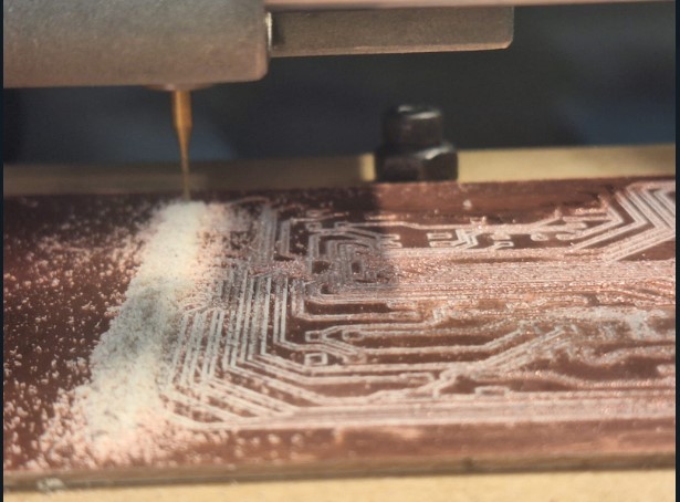
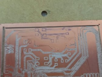
- As you can see, it took me different attempts to get a file that
worked, but once I had it, I also tried to use smaller tools for the
engraving step in order to prevent very slim traces.
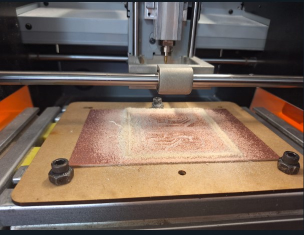
In the second picture you may see that I made a cutting/ callibration
test where I Let it carve my
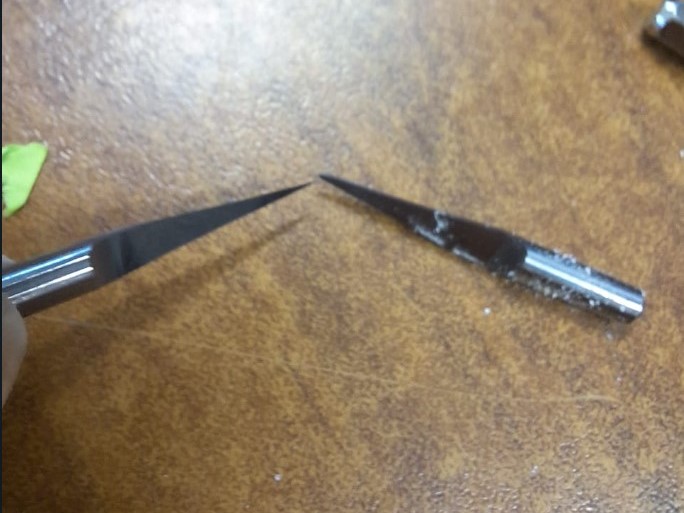
name, but there the tool recieved too much tension for it's diameter and
broke, that's why I decided to change the way I
calibrated the milling tool.
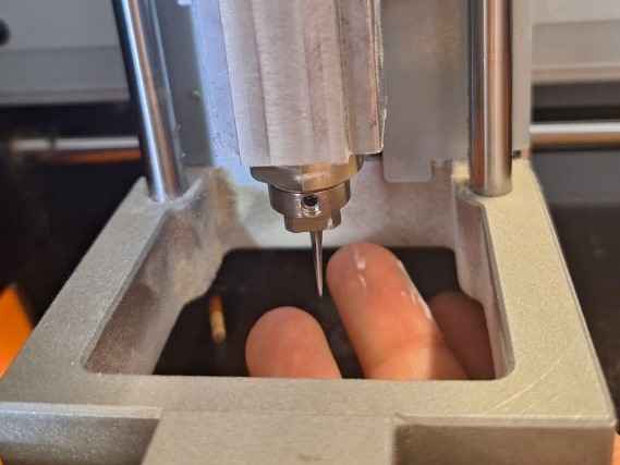
To adjust them I used a different thechnique: First I would attach the tool very loose and and lower it to the max, once it made contact with the surface of the copper, I secured it and tested the Spindle, this last step to make sure there was contact without risking to break more tools, if necesary I would lower the tool one micron or two.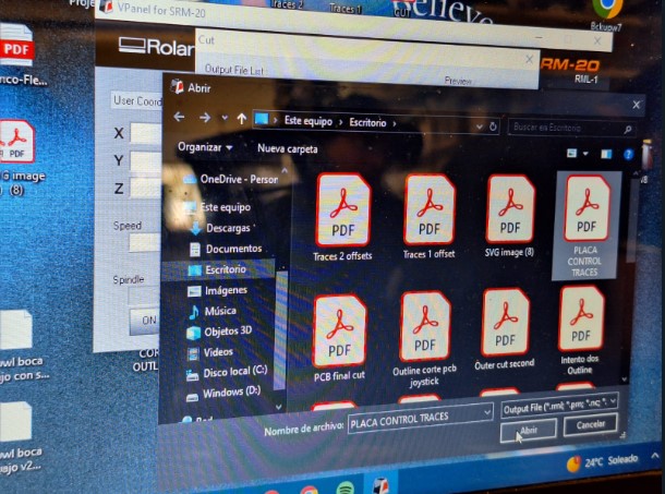
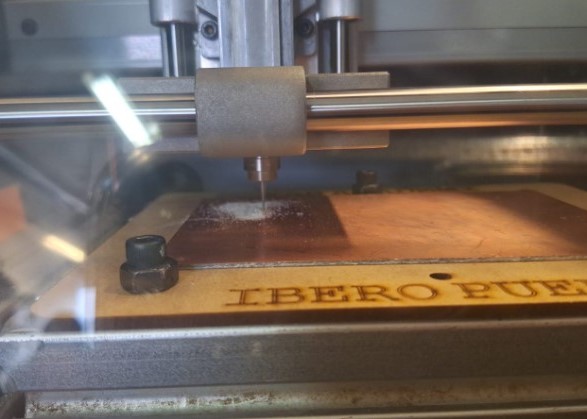
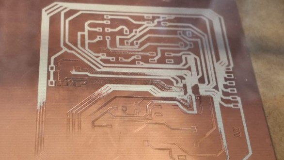
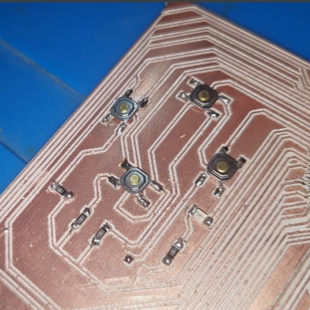
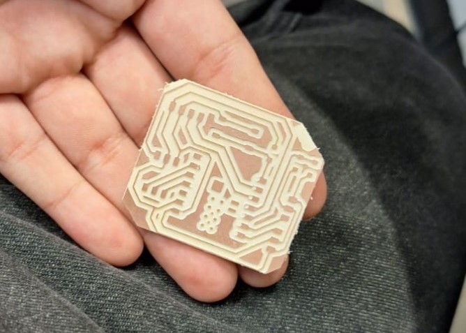
- Finally, after many attempts, the quality of the cut was good: not so deep, nor superficial, so I finally had a good board (or so I thought).
- Once I saw the final result, it was mostly perfect, despite at the right side, there where some traces where the tool only made superficial contact. Here I checked the optinos, because the board took about an hour to engrave and the machine was not so available so I had to be as practical as I could. The options were either try to cut it all again or find a way to cut what I needed.
In the end I decided to make the correction myself: with a pen I made a guideline to cut over the traces and with a manual cutter blade I cut it. Here I also concluded that probably the original cut failed only there because of the size of my board and the tension on the wood of the sacrificial bed. That was just an idea, but I didn't have trouble with smaller boards or saw anyone with something like that. I advise better cut smaller boards or put the origin closer to the middle.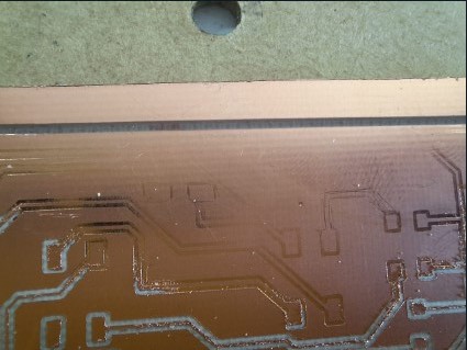
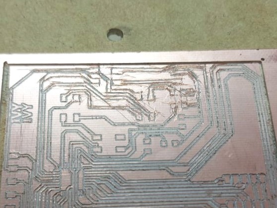
- As my manual cuts were less precise than the original ones, I used the multimeter to check continuity in tracks and make sure the ones that had to be connected still were as the separated ones had enough distance.
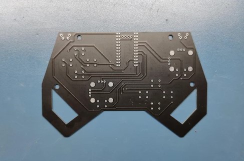
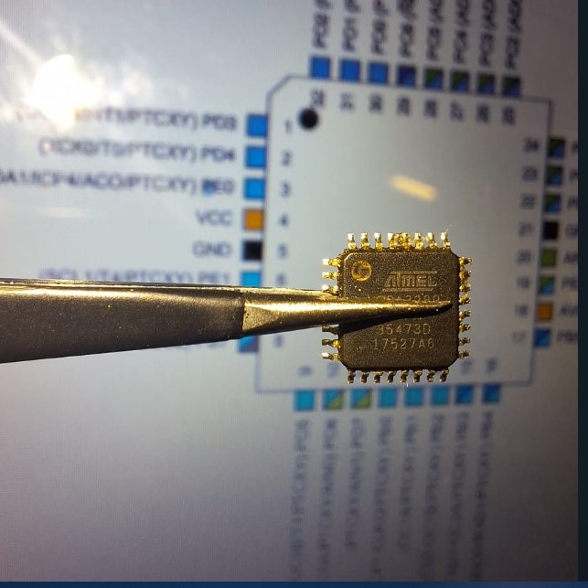
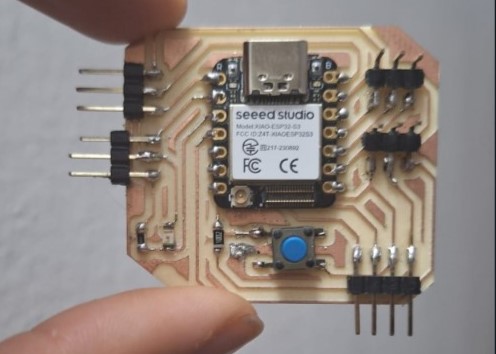
- Once I made sure I had everything clean, I started to gather my components to solder. My main microcontroller was an Atmega328, so I checked it's Pinout, soldered pins, resistors, LEDS and buttons.
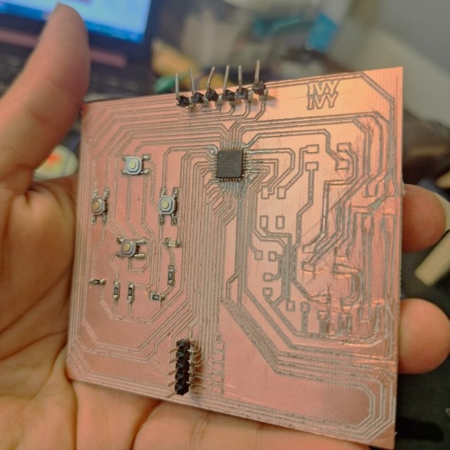
- After some trouble to solder the pins here, I decided to move from the original idea of single pins to solder them by pairs to give them more stability. This is the final result
Making THE board
As I made the first board, I noticed it was pretty ambitious but not so practical for further testing and the upcoming weeks, so I decided to make a new one that would work for the electronics weeks and also for my final project. That's why I call it "THE board". Even so, I kept it pretty simple to be conscious about my skills and learning stage. > Note: this board was made some weeks apart from the first one, so some design choices considerate other posssible boards from further weeks.
If you wish to know in which Weeks I used this board, here you may find them here: Getting startedThe first step to design my board was to understand the purpose of it. As stated before, I wanted a board that could be practical for assignments that require the usage of other modules, so pins were a must, not only for data but also to have enough to connect PWR and GND.
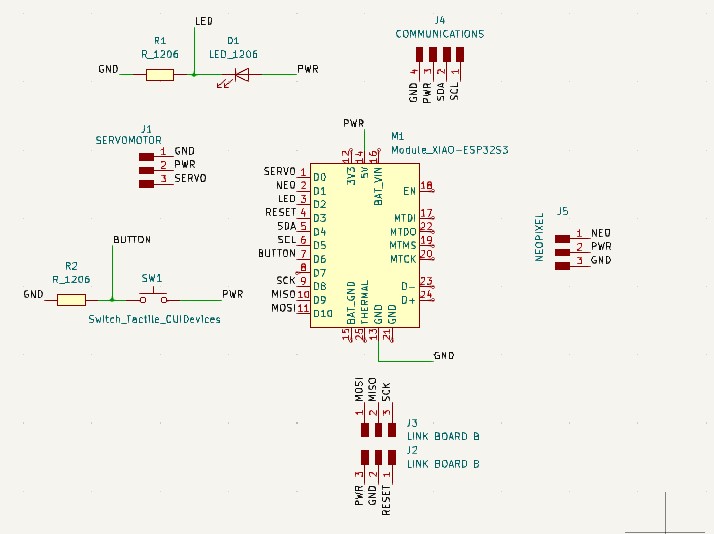
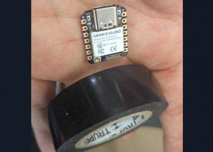
Next I thought about the main microcontroller, since I wouldn't require that many data pins, I already had experience programming some of them and it felt easier to use one that had an interface to connect it directly, I went for a XIAO. Also, at this moment I knew I would require bluetooth connection and I could use probably a camera, so the one was the ESP32S3. Now, let's see how I made it.- First, I started my schematic adding the elements from the library: My Xiao ESP32S3, a
"Status LED", and it's respective resistor. Then I realized I could use a button,
so put it two with it's resistor.
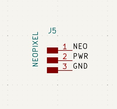
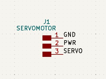
- Once placed, I started to think about the pins, I wanted my board to be as intuitive as possible without having to look at the schematic or PCB editor before soldering or programming. So that, I listed the modules I could need and how did they arrange their pins: a servomotor, a Neopixel, a buzzer, a joystick...Most of these use at least 1 Signal Pin , 1 Ground Pin and 1 Power Pin.. Keeping this in mind, I grouped at least 3 pin holders and named them based on the module I expected to go there.
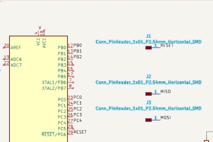
- Then, I also acknowledged that most probably I could use another board for my final project, and that probably wouldn't have an USB port, so I would need to use another board as a programmer. That way, I included another set pins to program a board: MISO,MOSI,SCK,RESET,GND,PWR. Also, considering this, I made another set to manage the board's pins for communication: SCL, SDA
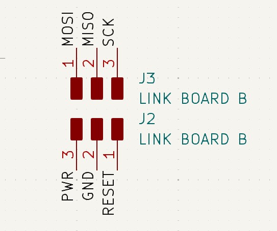
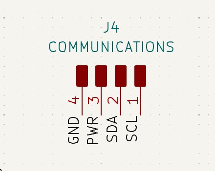
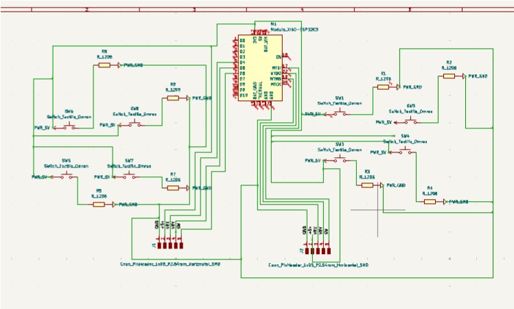
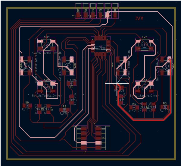
- Next I did, was assign tags to my components to keep everything connected. This is how the schematic looks like in the end
- Next thing I did was to connect everything and export the SVG files for the traces and the outline to cut them. editor.
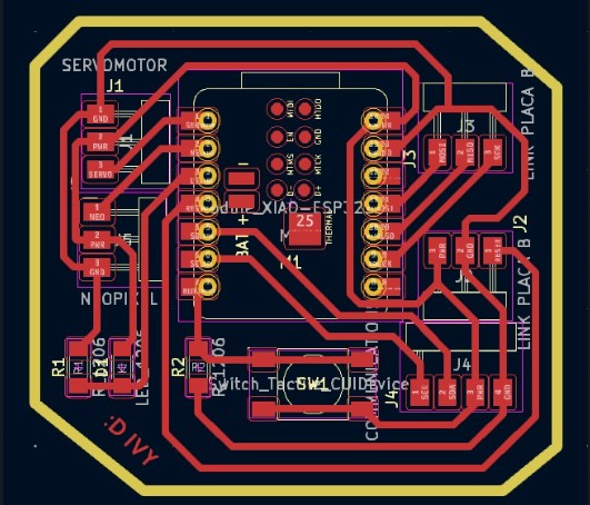
- Then it was time to prepare the files in MODS. As in the previous board, I first selected 1/64 for traces and 1/32 for the outline. Also, the tools I chose were .4mm for Engraving and 1mm for cutting.
- Now I had to prepare everything to cut! The Traces came out perfectly smooth at the first attempd, so that's the main reason I wanted to document this in this site and not the one of the final project: so you can see the before and after my skills to calibrate the Roland and the bed. Despite my name got erased everything else worked just fine! Irecommend to reduce the offset and maybe make the traces thicker.
Fun fact: I set the cutting tool to be 1 mm at the mods, but in my FAB we didn't have anymore when I already had cut the traces, the only ones left were 2mm. As I didn't want to risk damaging the board because the outline was very close to some traces or, I took the risk to cut the outline with a engraving tool that was already broken, so its edge was almost 1mm. I made some pauses inbetween the cut to keep caution, but in case you don't have a cutting tool a broken engraving one can do the job really nicely!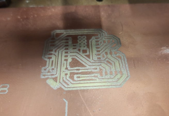
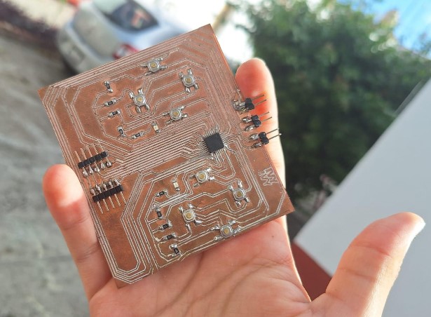
- The next step now was to solder everything. Note: If you're not using the pins on the back of the XIAO cover the back with insulating tape. Here you can see the final result of this PCB!
Testing!
To check that the board and it's connections worked as I wanted, I charged a classic blink Code from the Examples of Arduino IDE on it. It was functional!
---- Files ----
-
Of the first board (Controller)
-
Design Files
-
SVG Traces
-
SVG Outline
-
Of "THE" Board (Main ESP32S3 board)
-
Design Files
-
SVG Traces
-
SVG Outline
- Once placed, I started to think about the pins, I wanted my board to be as intuitive as possible without having to look at the schematic or PCB editor before soldering or programming. So that, I listed the modules I could need and how did they arrange their pins: a servomotor, a Neopixel, a buzzer, a joystick...Most of these use at least 1 Signal Pin , 1 Ground Pin and 1 Power Pin.. Keeping this in mind, I grouped at least 3 pin holders and named them based on the module I expected to go there.
- Finally, after many attempts, the quality of the cut was good: not so deep, nor superficial, so I finally had a good board (or so I thought).
- I used the parameters of 1/64 for the traces and 1/32 for the cut. Also, as my microcontroller was very small I gave the tool a very thin diameter.
- After updating, It showed me the pieces all together, The blue lines are the preserved links between components I had from the schematic. Note: If something is not linked visually by a blue line here, it won't allow you to join the components with trcks.
- Then I added a resistor to each button, and placed them on the upper right corner