9. Ouput Devices
WHAT IS AN OUPUT?
Output devices are any peripherals that receive data from a computer and print, project, or replicate it. The output might be audio, video, hard copy - printed paper, etc. Output devices translate computer data into human-readable form
Pulse Width Modulation
Pulse width modulation (PWM) provides a way of controlling certain analog quantities, by varying the pulse width of a fixed frequency rectangular waveform.
PWM generates square-wave pulses of varying widths. The pulse width offset, which is proportional to the amplitude of the input signal, can be controlled using PWM. PWM is commonly used to control motors, power LEDs, regulate voltage, and modulate communications. Its main advantage is that it allows for precise control of the average power delivered to a load or output.
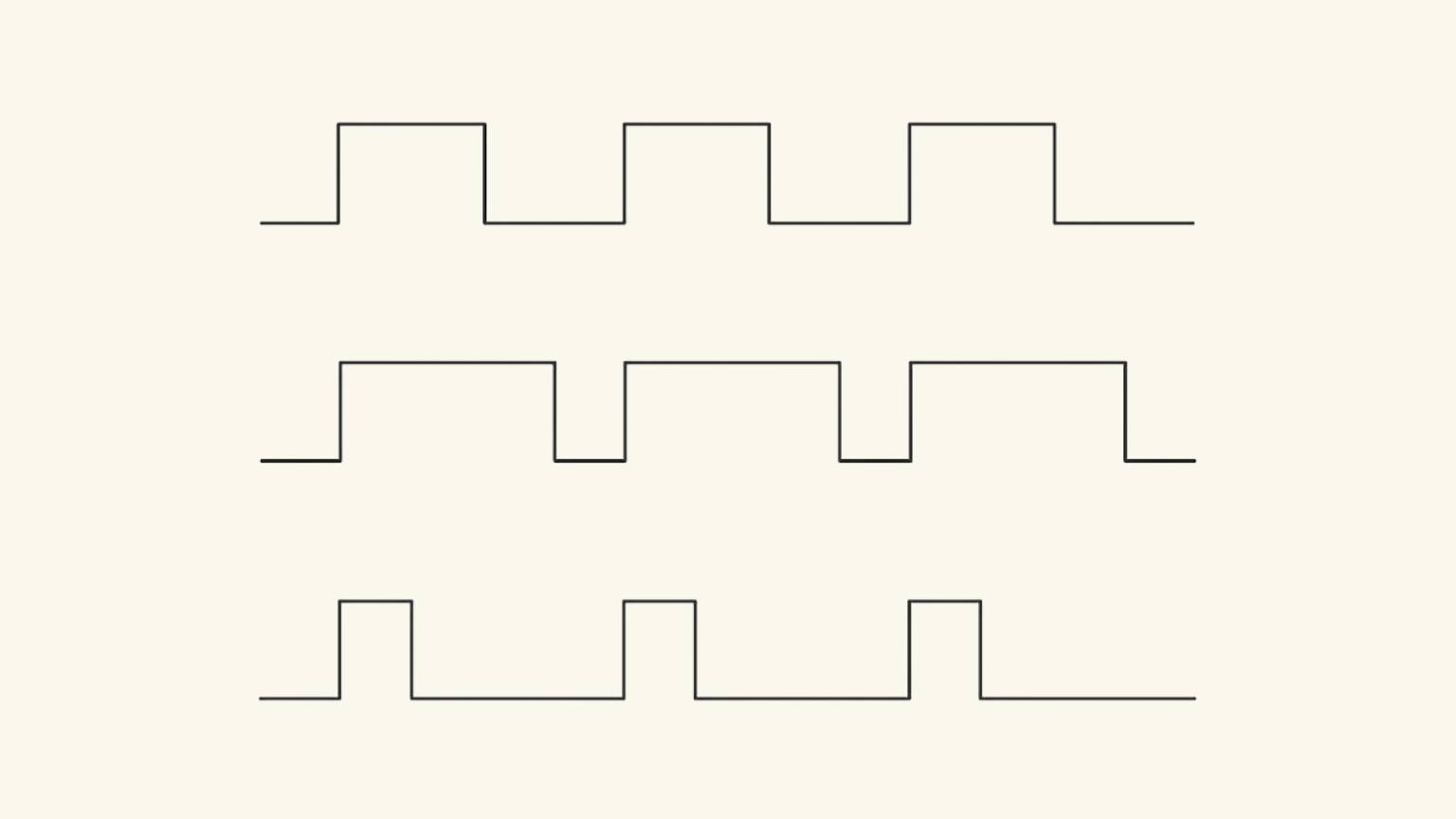
PWM Signal Waveforms by CircuitBread
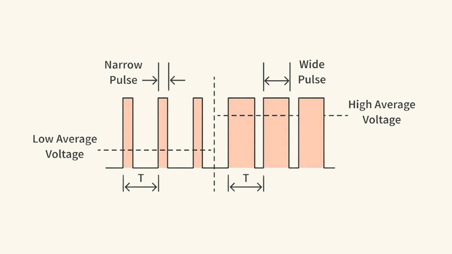
Pulse and time period of a PWM signal by CircuitBread
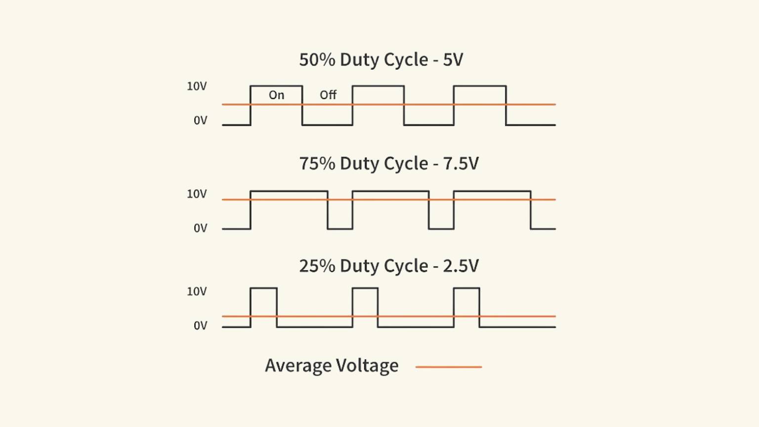
Different duty cycles and their average voltage by CircuitBread
Types of output devices
| Device | Description | Image |
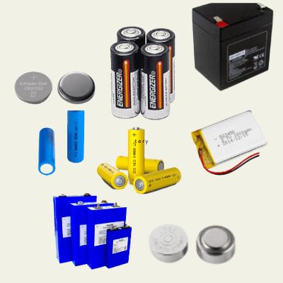
| Battery | A battery is a device that stores chemical energy and transforms it into electricity. This is referred to as electrochemistry, and the system that supports a battery is termed an electrochemical cell. A battery can consist of one or many electrochemical cells (as in Volta's original pile). Each electrochemical cell has two electrodes separated by an electrolyte. |
|
| Servo | Servo motors are components of a closed-loop system that include a control circuit, servo motor, shaft, potentiometer, driving gears, amplifier, and
an encoder or resolver.
|
 |
| Buzzer | An audio signaling device, such a beeper or buzzer, can be electromechanical, piezoelectric, or mechanical. Its primary job is to transform audio signals to sound. It is commonly powered by DC voltage and found in timers, alarm devices, printers, computers, and other equipment. It may emit a variety of sounds, including alerts, music, bells, and sirens. | 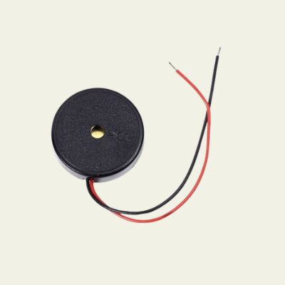 |
| Speaker | Speakers are transducers that convert electromagnetic waves to sound waves. They are used to output audio from computer systems. Users can input audio in either analog or digital format to generate analog electromagnetic waves (analog speakers) and sound waves. |  |
| OLED | OLEDs are organic LEDs. Organic compounds derived from carbon serve as their primary building components. Unlike LEDs, OLEDs are diffuse-area light sources manufactured in sheets, rather than small-point light sources. | 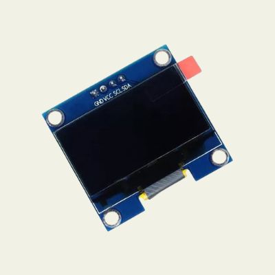 |
Group Assignment
Visit our group task by clicking on the button below.
What did I do this week?
Note:This week, I struggled to understand the topic, leading to days of regret, frustration, stress, and improvisation. I did a lot of tests, I tried a lot of things, I failed a lot, and up until this moment, I have not been able to get my OLED screen to turn on. Overall, this has been my most challenging week yet, and I am dissatisfied with both my process and final delivery.
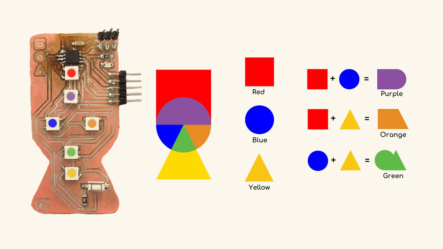
I decided to utilize a display to showcase the symbols that had inspired my prior PCB design. I'd want to show the association between colors and shape.
To do this, I've done five distinct things:
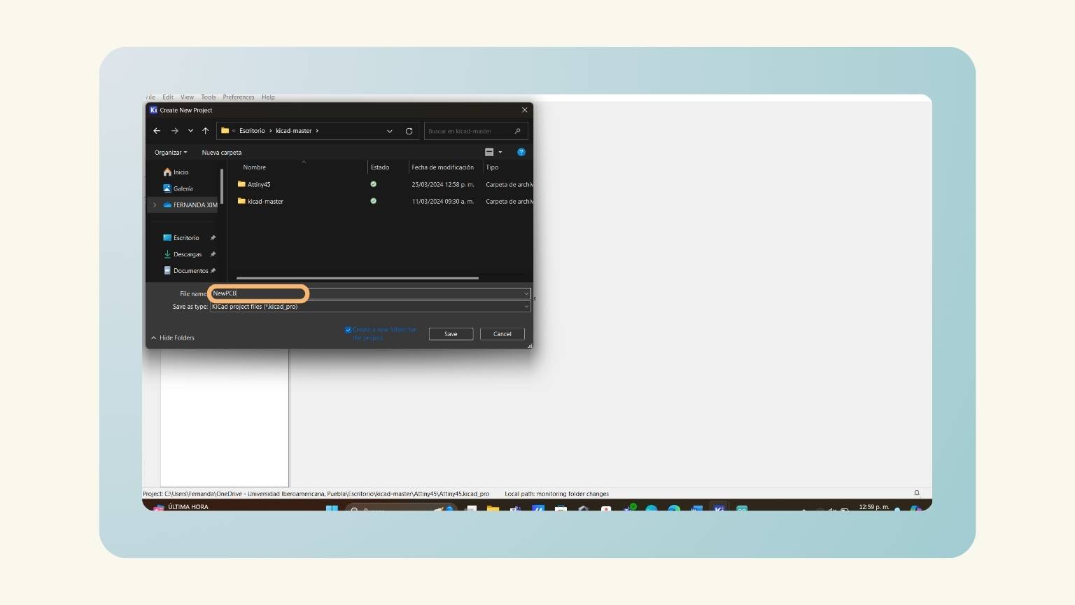
1. PCB Design
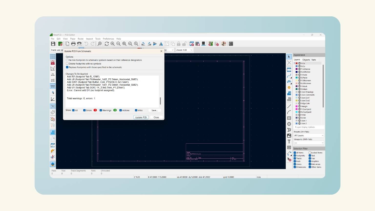
I created a new PCB because I didn’t have the necessary pins on the previous one.
- So, I opened KiCad to design the new PCB.
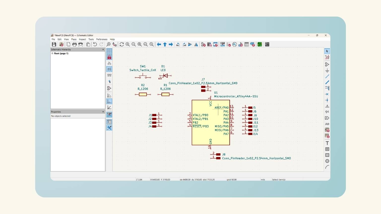
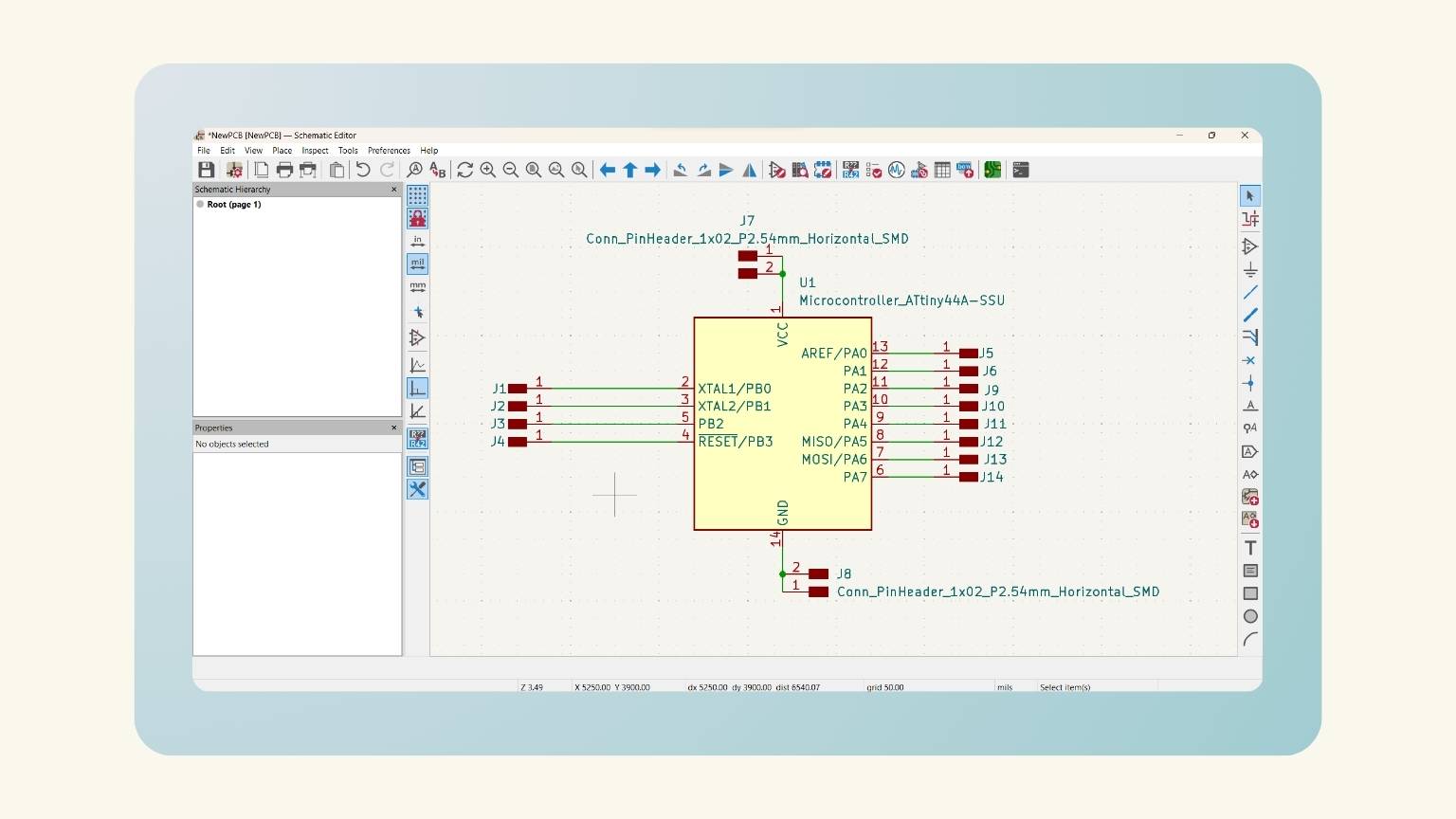
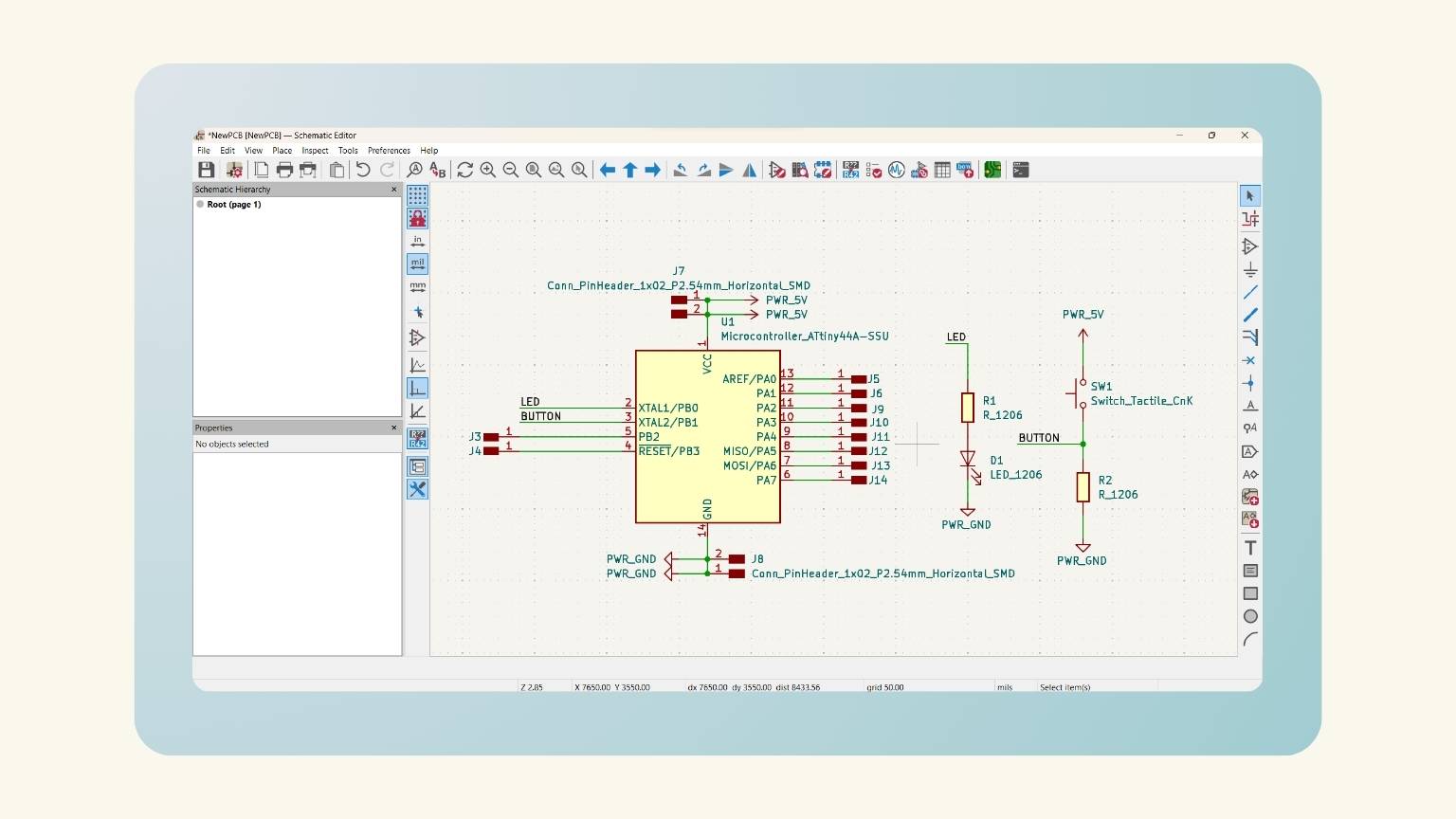
- I added all the components that I needed.
- I added the power symbols and connected them with the respective components.
- Then I made the connections between the components. .
- I passed it on to the PCB editor to complete the design.
- I updated the PCB from the schematic.
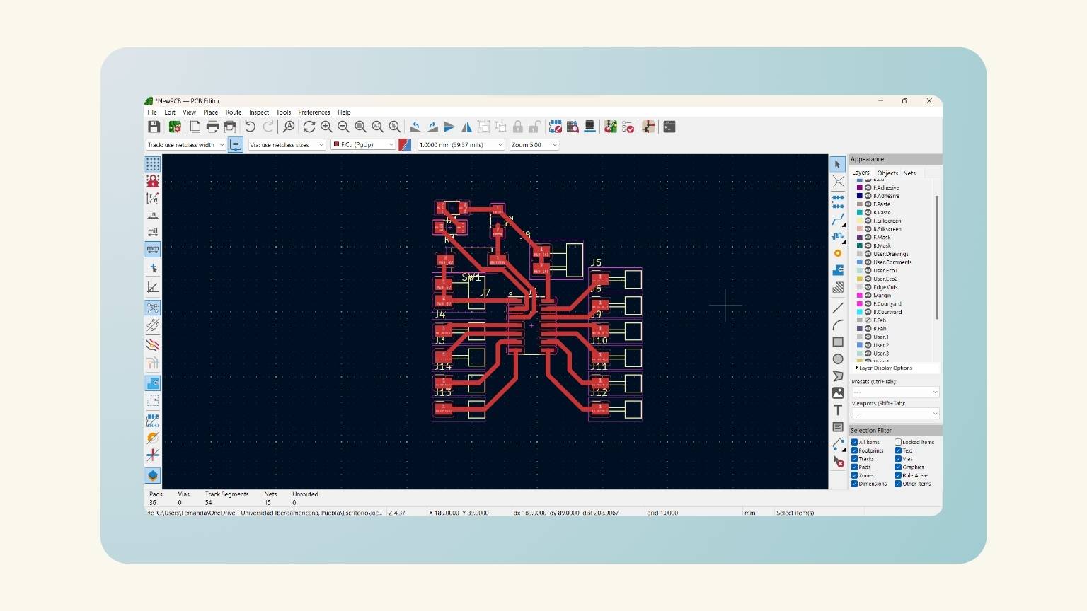
- I organized the components to make the traces and connections.
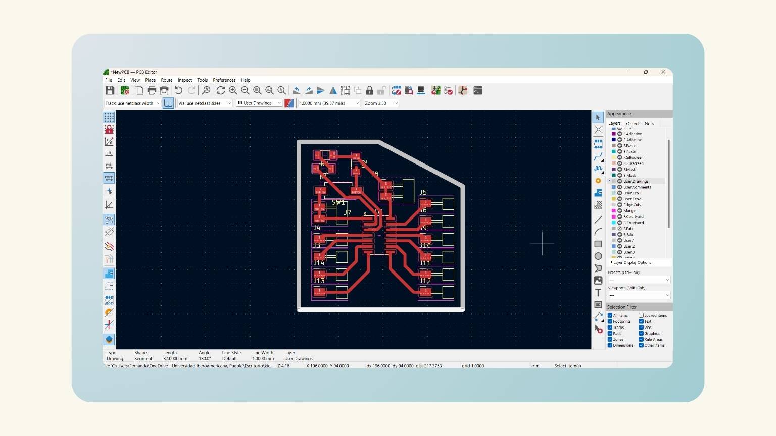
- I made the framework.
- Next, I saved the strokes first, and then the outline.
2. PCB Production
Recap
The machine used for the creation of the PCB is...
ROLAND SRM-20
This machine can cut a broad range of materials, including chemical wood, acrylic, and ABS. It also supports a wide variety of accuracy settings, from prototype to product design. Furthermore, its tiny size and fully enclosed design allow you to cut with greater safety and confidence.
What tools will we use?
V-Cutter, allows for better engraving for its fine tip.
Flute end Mill, for drilling and plate cutting.
To prepare the control software, I used...
Mods
A program that allows me to extract G-codes or machine codes from images, vectors or 3d models.
So, when I have my PCB design, I have to save it…
but how did you save it?
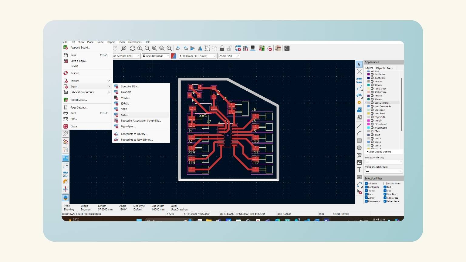
- I went back to the KiCad PCB Editor and went to the ‘File’ menu, subsequently to 'Export', and selected the ‘SVG’ option.
- The ‘Export’ menu was displayed, and I selected the layer I wanted to save. In this case, I first saved the strokes that were inside the
‘Copper layers’, which have the name ‘F.Cu’.
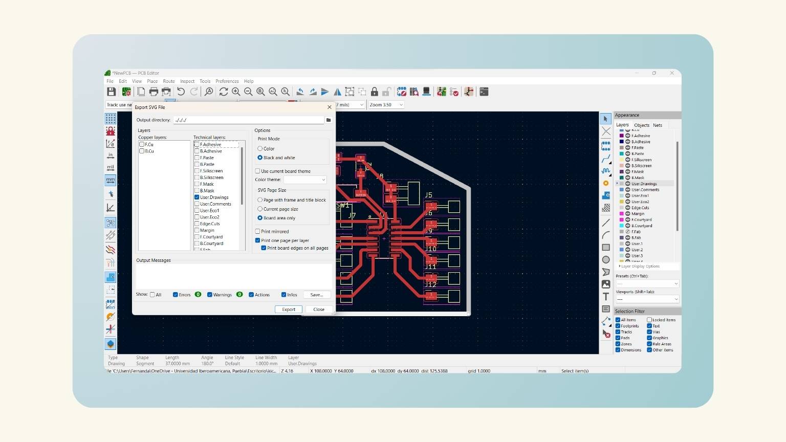
- In the options, I selected the ‘Black and white’ print mode and the ‘Board area only’ SVG Page Size. Then I pressed ‘Export’.
- After, I did the same, but I changed the strokes layer to the cut later; in my case, it was the ‘User.Drawings’ layer.
- And I have the two files to cut!

Mods Time
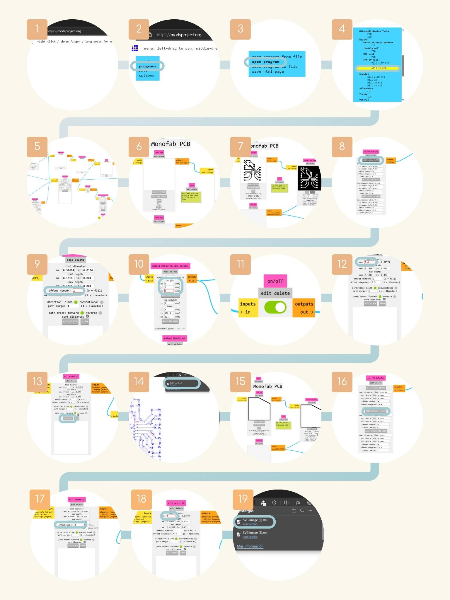
- I opened the MODS web server.
- I right clicked on ‘Programs’
- Next in ‘Open program’
- I searched the program of the SRM-20 mill machine and selected the ‘mill 2D PCB’.
- All the blocks to be worked on are displayed to obtain the corresponding files.
- The first block that I modified is the 'read SVG’ block for selecting a SVG file.
- I saw that the image was uploaded to the server.
- I moved to the ‘set PCB defaults’ block and pressed ‘mill traces’.
- I moved to the ‘mill raster 2D’ block. And I changed the ‘offset number’ to two.
- Then, I went to the ‘Roland SRM-2D milling machine’ block, and I modified the origin of the machine. For this, I changed the numbers on the axes x, y, and z.
- I moved to the right and turned on the ‘outputs’.
- I moved to the ‘mill raster SD’ and changed the tool diameter to 0.4 mm.
- And then I pressed ‘calculate’.
- And I saw a preview. In addition, in my downloads, I found an archive ‘.png.rtl’; this is the file that I opened on the machine.
- Next, I did the same steps with the SVG of the cut. Starting by selecting the cut SVG of my files.
- I moved to the ‘set PCB defaults’ block and pressed ‘mill outline’.
- Then, I went to the ‘mill raster 2D’ block and changed the ‘offset number’ to one.
- I moved to the ‘mill raster SD’ to change the tool diameter to 1 mm.
- And I pressed calculate to see the preview of the cut and downloaded the file for the machine.
Cut Time
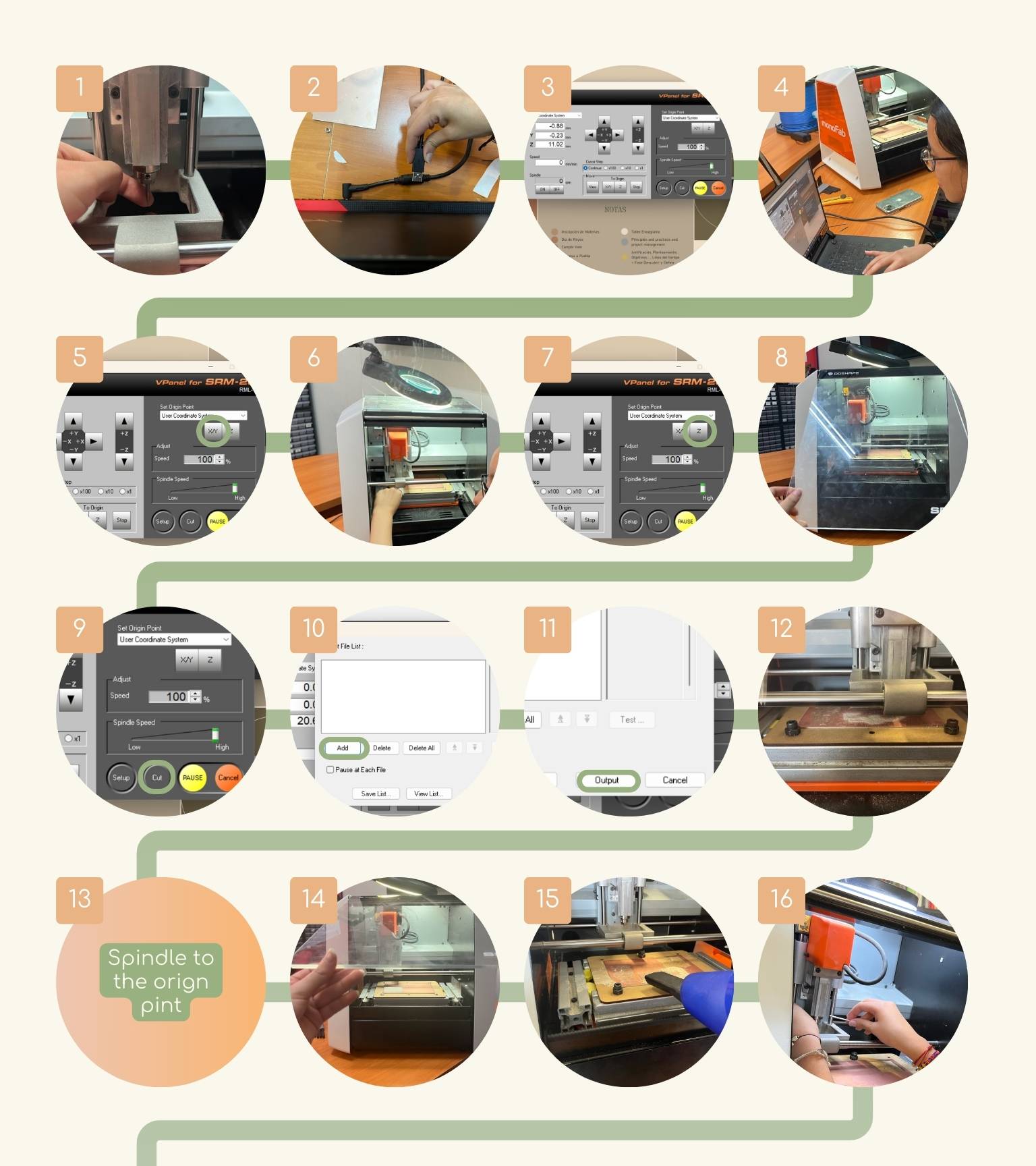
- I placed the tool, a 15 degree V-bit, to make the engraving.
- To do this, I used a wrench to tighten the tool.
- Note:Make sure that only the conical part of the tool protrudes.
- I connected the machine to my computer.
- I open the ‘VPanel for SRM-20’
- First, I moved the X/Y axis to the lower left of the material.
- And I pressed the ‘X/Y’ bottom to change the origin of this axis’s.
- Then, I moved the Z axis. To do this, I used a piece of paper to make sure I put the axis at the correct height.
- For this special axis, I used a paper to define the distance between the tool and the material. I did this by placing the paper on the material and lowering the tool a little at a time until the point where friction is generated and the paper gets stuck.
- Note: In this axis, before we did the paper check, we had to turn on the spindle and lower the z-axis, giving only one click to selecting ‘x10’ in the cursor step.
- I save the origin of the axis by pressing ‘Z’.
- When I defined the axis of origin, I closed the door of the machine.
- Then, I pressed the 'Cut' button at the bottom of the panel.
- I added the file to be engraved.
- I pressed ‘Outpt’ to send the file to be engraved.
- And the machine started to engrave.
- When the engraving was finished, the spindle went to the origin point.
- I opened the door of the machine.
- I used a hand vacuum cleaner to remove the dust produced by the engraving.
- I removed the tool that the machine had because it wasn’t the right one.So, I changed the previous tool to do the cut.
- For this, I used a wrench to tighten the tool.
- Note:Make sure that the conic part protrudes.
- I maintained the ‘X/Y’ origin and only changed the ‘Z axis’ because the tool was different and it was necessary to reconfigure that axis due to the height of the tool.
- I save the new origin of the axis by pressing ‘Z’.
- When I closed the door of the machine, I pressed the ‘Cut’ button to delete the previous file that I added.
- I added the new file of cut. And I pressed ‘Output’ for the machine to execute the cut.
- The machine started the cut.
- I used a hand vacuum cleaner to remove the dust produced by the cut.
- I removed the screws fixing the material with the help of a screwdriver.
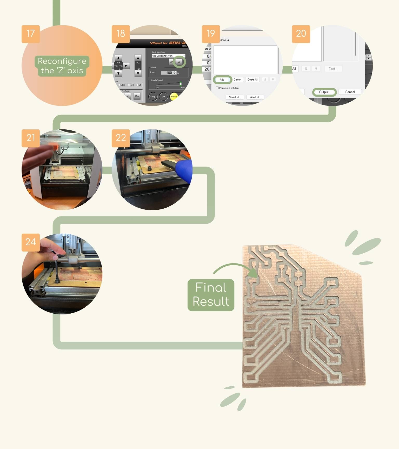
- Finally, I had my newPCB!
Note:To move the axis fist, I used the ‘Continue’ cursor step, after the ‘x100’ (1 mm), then the ‘x10’ (0.1mm), and finally the ‘x1’ (0.01mm) until the paper generated friction and didn’t come off.
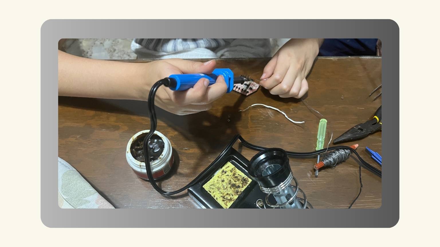
3. Soldering... here we go again
Notes:
- The Easter vacation in Mexico began on Saturday, so being a foreigner, I decided to go home and work from here. So, what you see below may not be the best practice, but everything went as well as it could have gone.
- Because of time constraints and other issues that caused me to work outside of Fab's schedule, I decided to purchase a pencil soldering iron, a soldering iron base, and other necessary materials. While it may not be possible to have an optimal workspace, my family and I are doing our best to make it work.
- Last week, my experience was complicated, and I won't lie, I was nervous about soldering a microcontroller like the Attiny again.
However, I had to do it... So I started soldering.
Soldering time
- I started to put a bit of soldering in the spaces destined to place the pins of the attiny.
- I placed the attiny on top and welded one leg first before moving on to the next pins to make the process easier.
- Then, I soldered the pins to which each pin of the microcontroller will be connected.
- The pins were solder!
- Then I soldered two resistance one to a button and the other to a LED.
- And finally, I soldered the button and the LED.
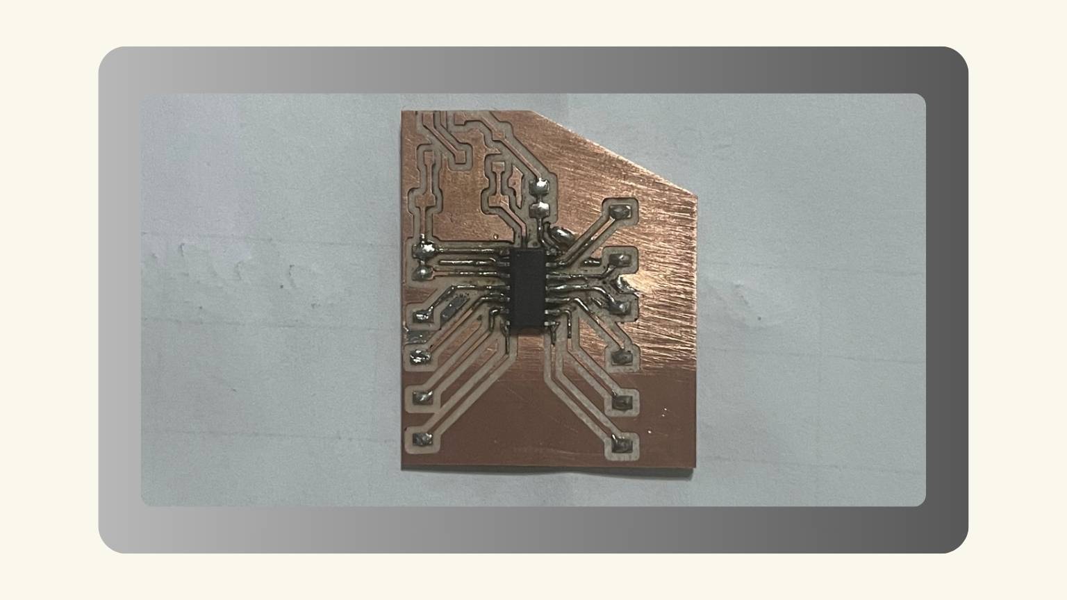
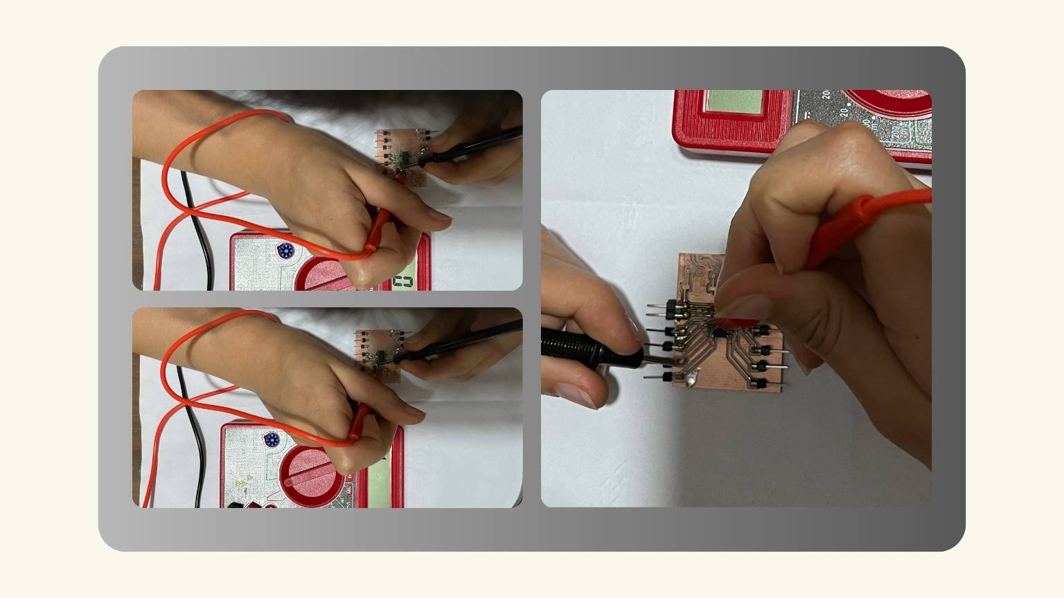
3.1. Multimeter Test
What is a multimeter?
A digital multimeter (DMM) is a flexible electronic instrument that can test a variety of electrical characteristics such as voltage, current and resistance. The measurements are shown on a digital screen, making them easier to read and comprehend precisely.
So, I used this tool to check that all the connections were good.
4 & 5. Programming and Trying
In this part, chaos started.
So, what happened?
First Try
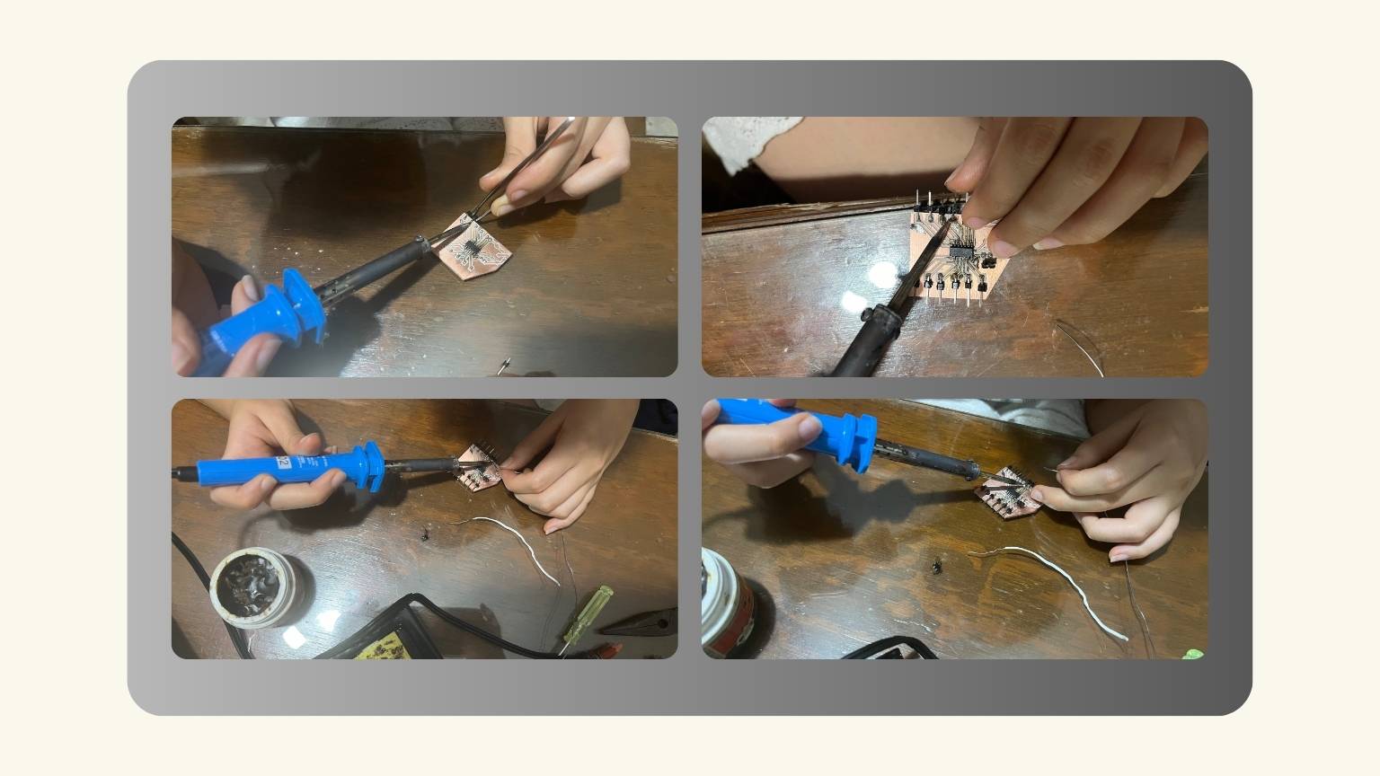
At this point I don’t know why I made another PCB… but I made it.
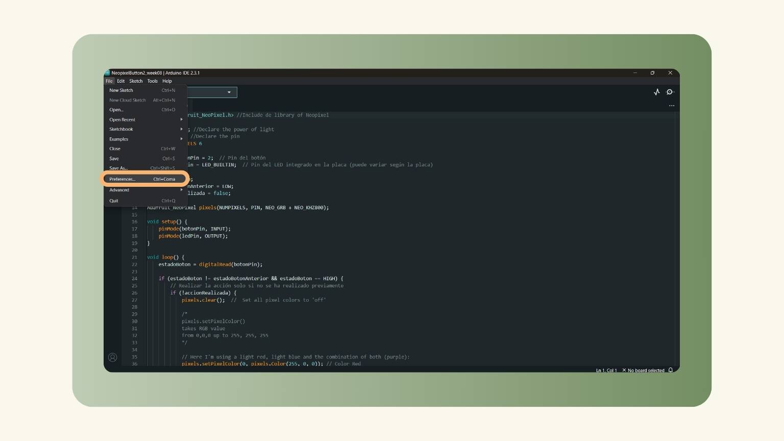
So, first, I tried to program the OLED with my new PCB. To do this, I have to burn the bootloader.
These were the steps:
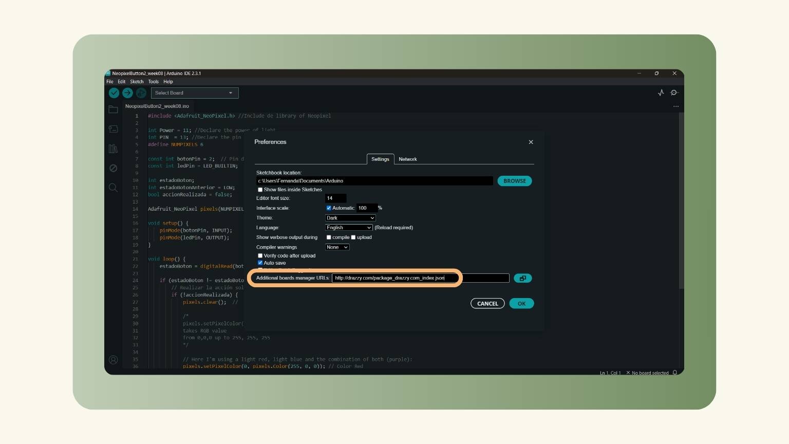
- I opened Arduino.
- I selected the ‘File’ menu and clicked on ‘Preferences’.
- Then I paste the next link to the section of ‘Additional boards manager URLs’. http://drazzy.com/package_drazzy.com_index.jso
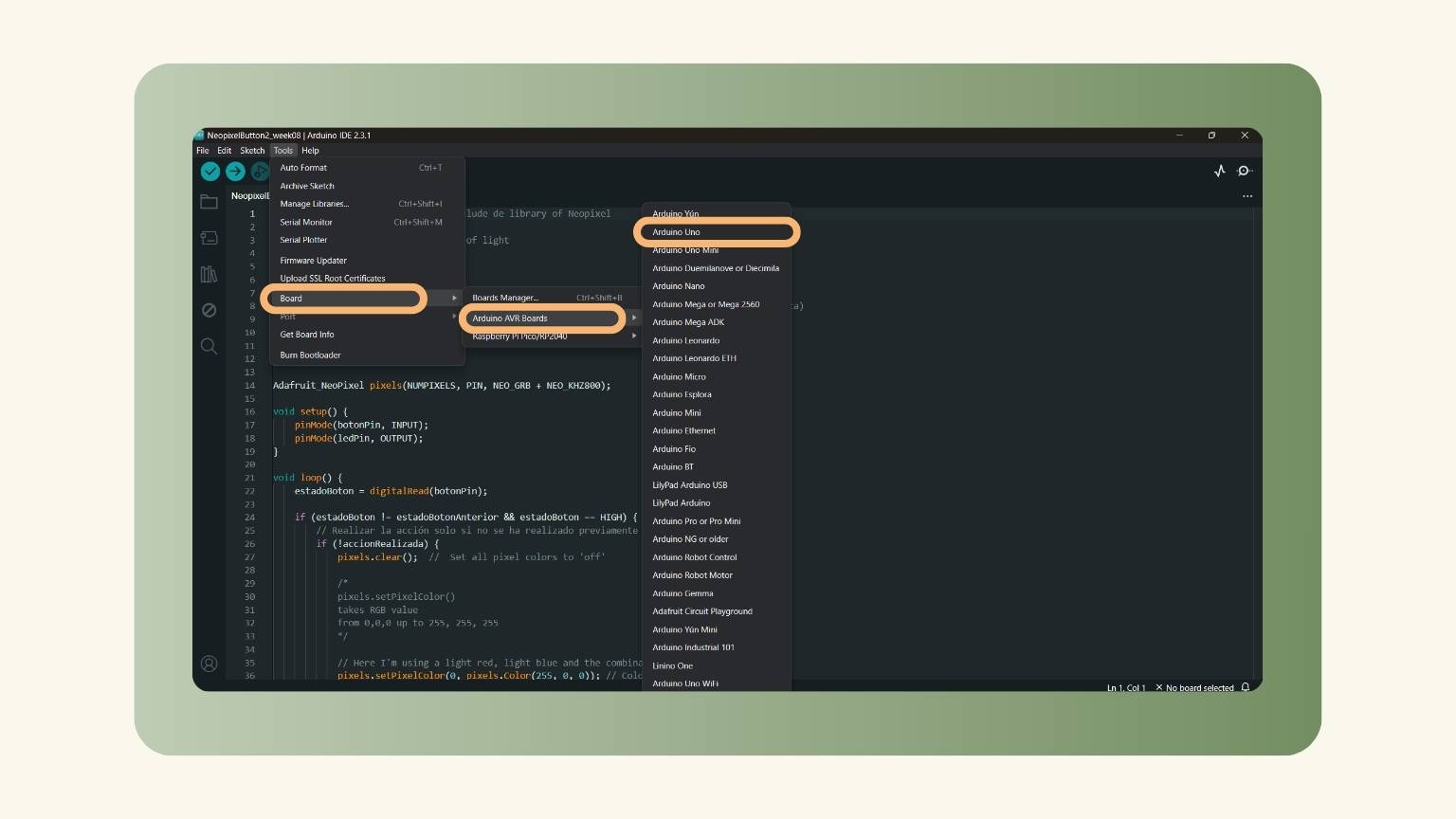
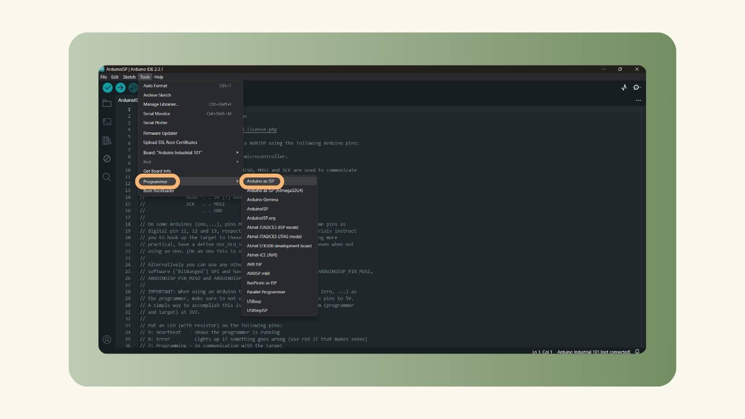
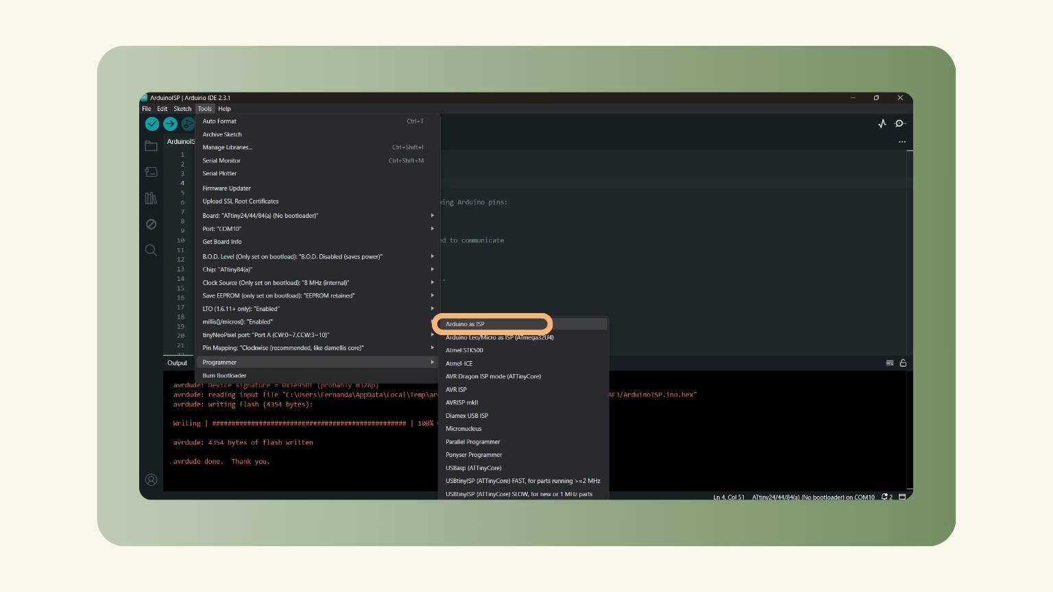
- I pressed 'OK', and then I went to the ‘Tools’ menu to select ‘Board’, after ‘Arduino AVR Boards’ and finally ‘Arduino Uno’.
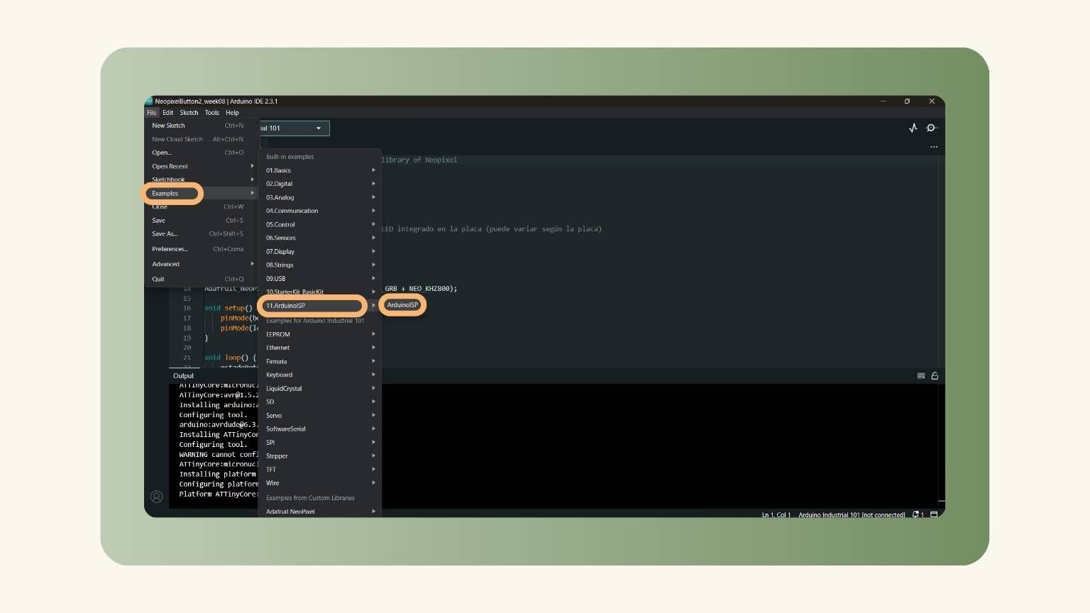
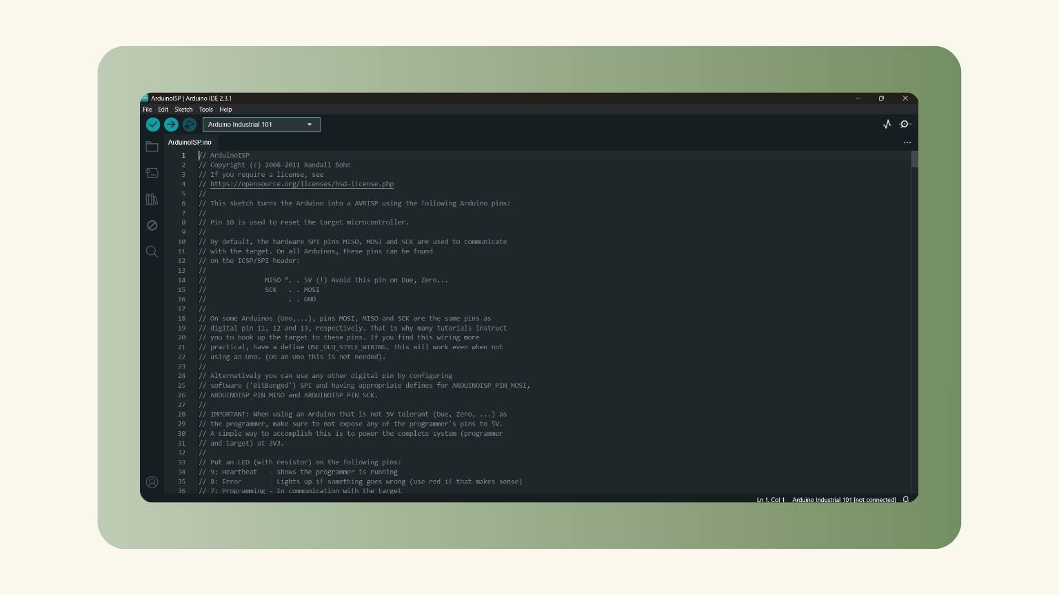
- Next, I went to the ‘File’ menu to open the example of ‘ArduinoISP’.
- The example was open.
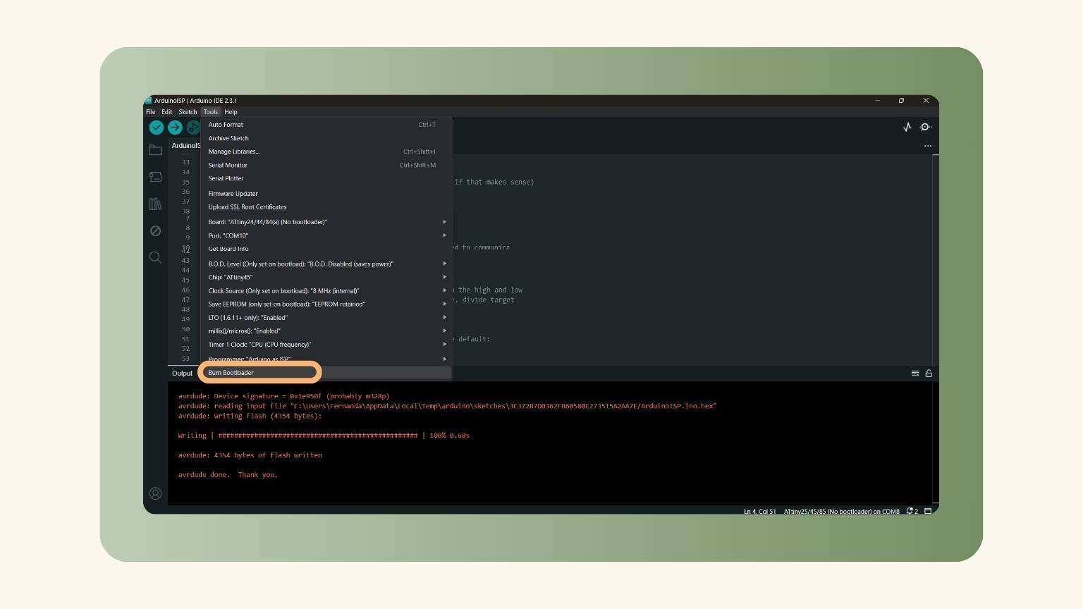
- I selected the ‘Tools’ menu to select the ‘Programmer’ option and pressed the ‘Arduino as ISP’.
- I uploaded the ArduinoISP example code.
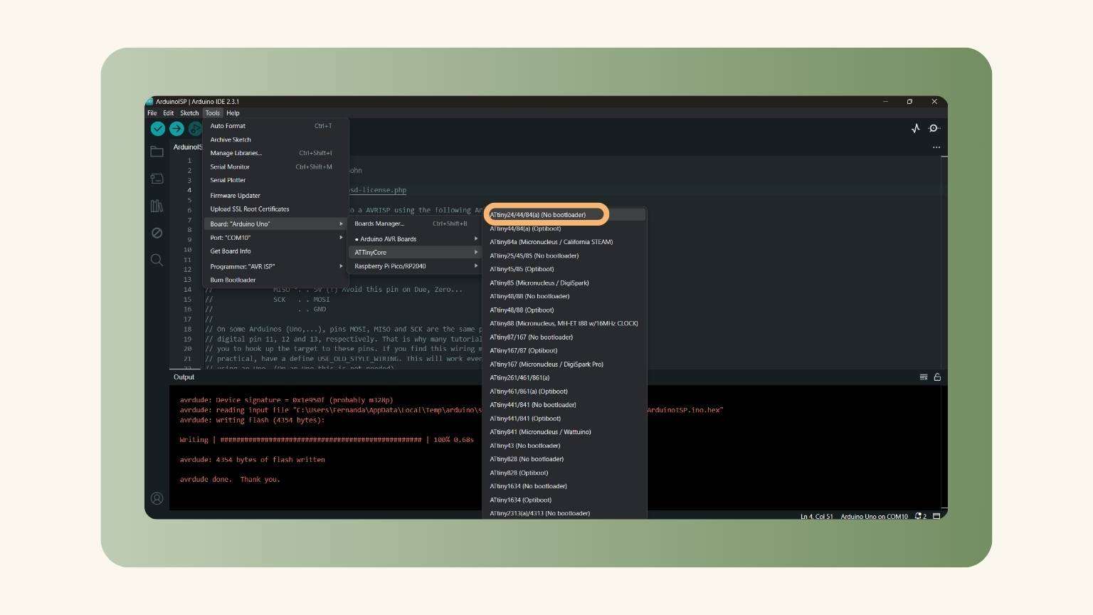
- Then, in the same menu, I selected the ‘Board: “Arduino Uno”’ and chose the ‘ATTinyCore’ to specify the ‘ATtiny25/45.85 (No bootloader)'.
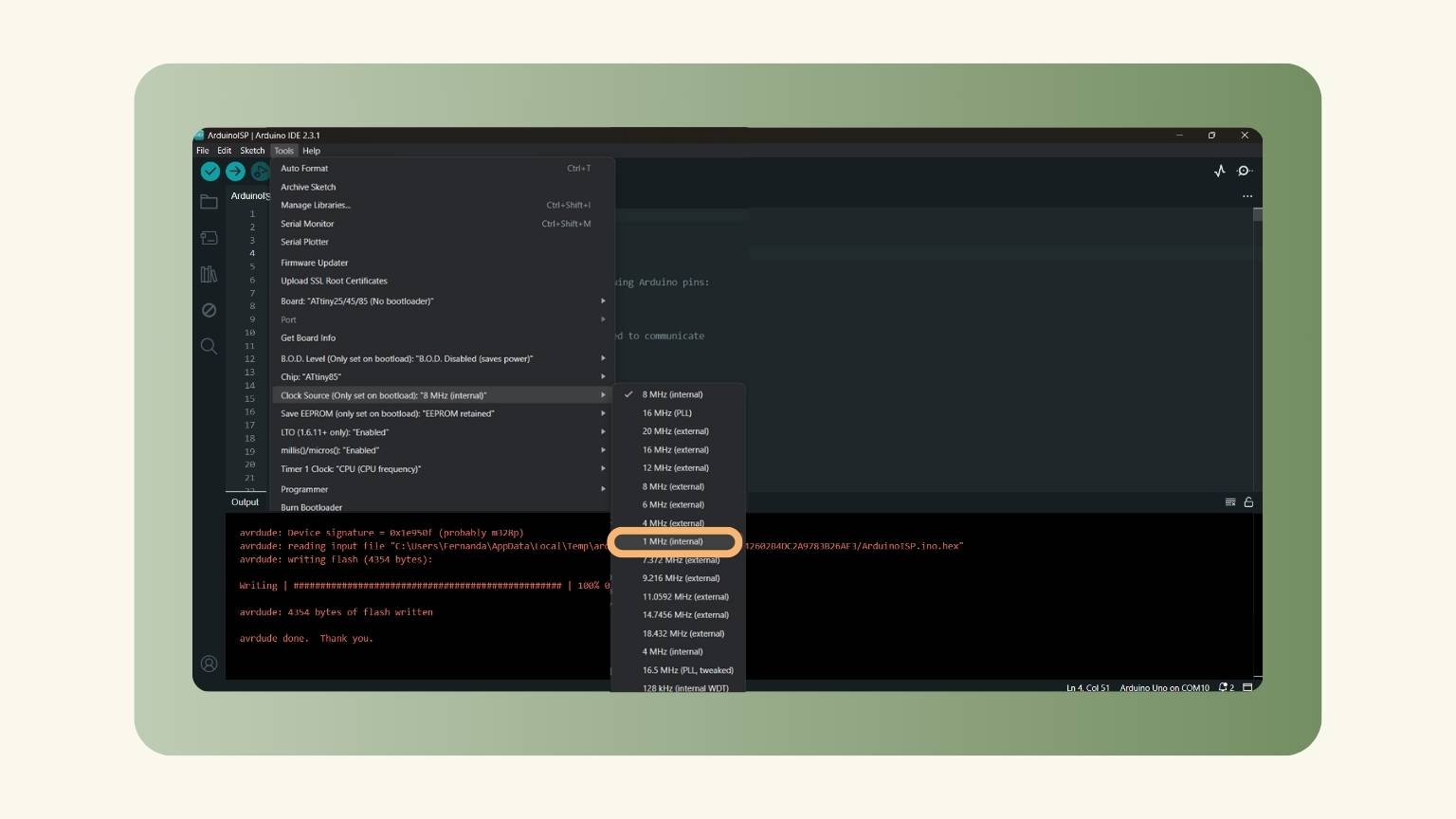
- I selected the ‘Clock Source’ option to select the ‘1 MHz (internal)’ option.
- Note: You will change to ‘8MHz(internal)’.
- I selected the ‘Arduino as ISP’ programmer in the ‘Tools’ menu.
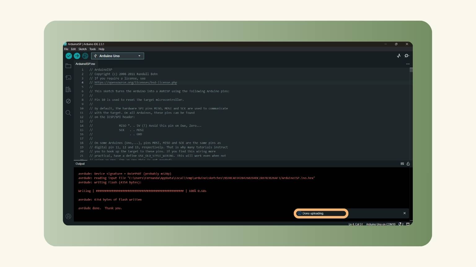
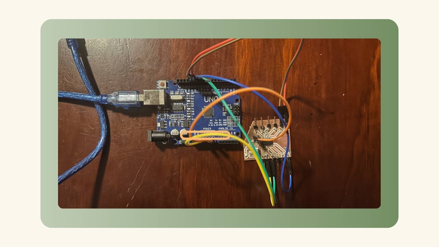
- I connected the Arduino to my PCB.
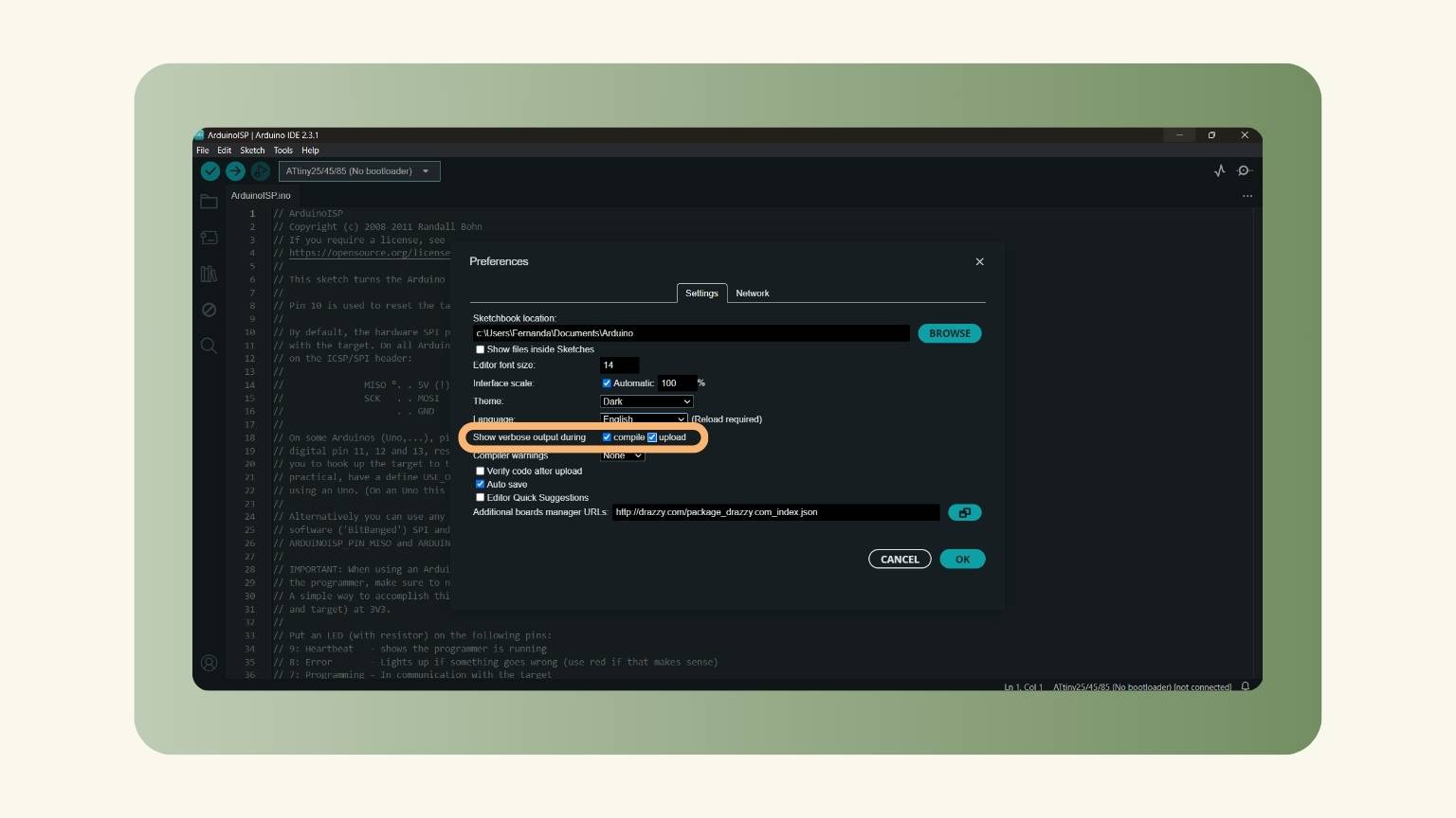
- Then I opened the ‘Preferences’ menu to select the two options in the ‘Show verbose output during’.
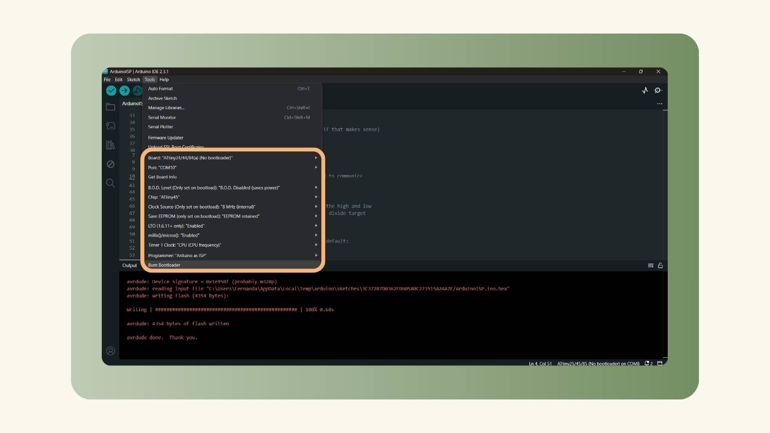
- In the ‘Tools’ menu, I checked that the options were good.
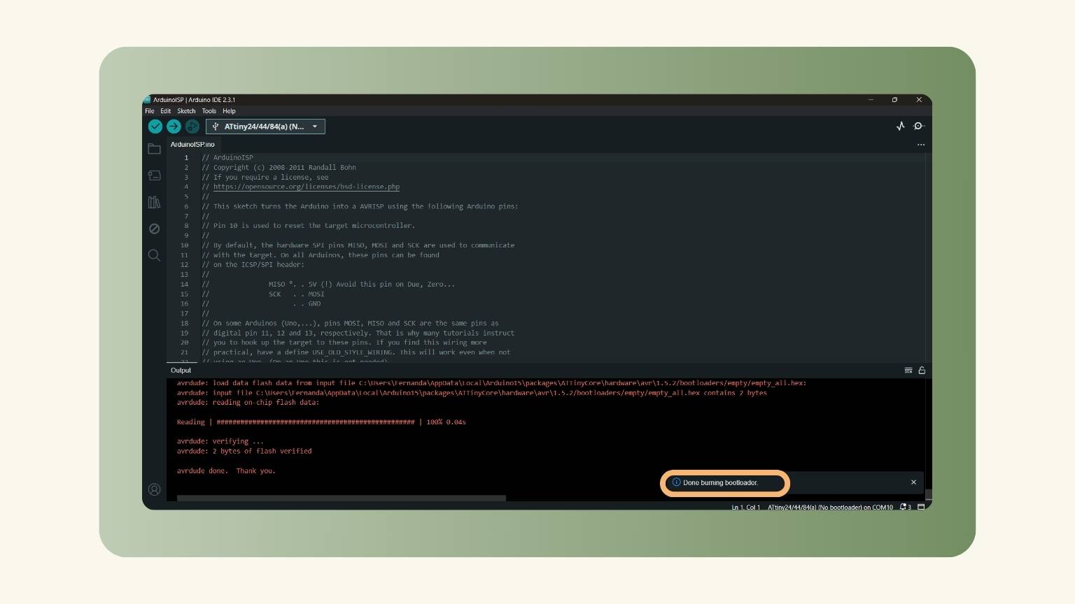
- I selected the ‘Burn Bootloader’.
- The burning bootloader was done.
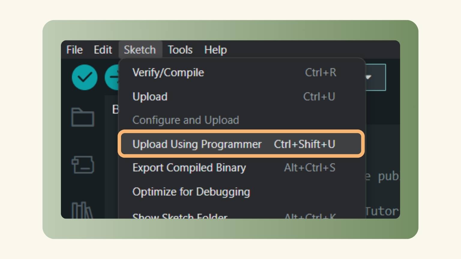
- I uploaded the file with the ‘Upload Using Programmer’ option in the ‘Sketch’ menu.
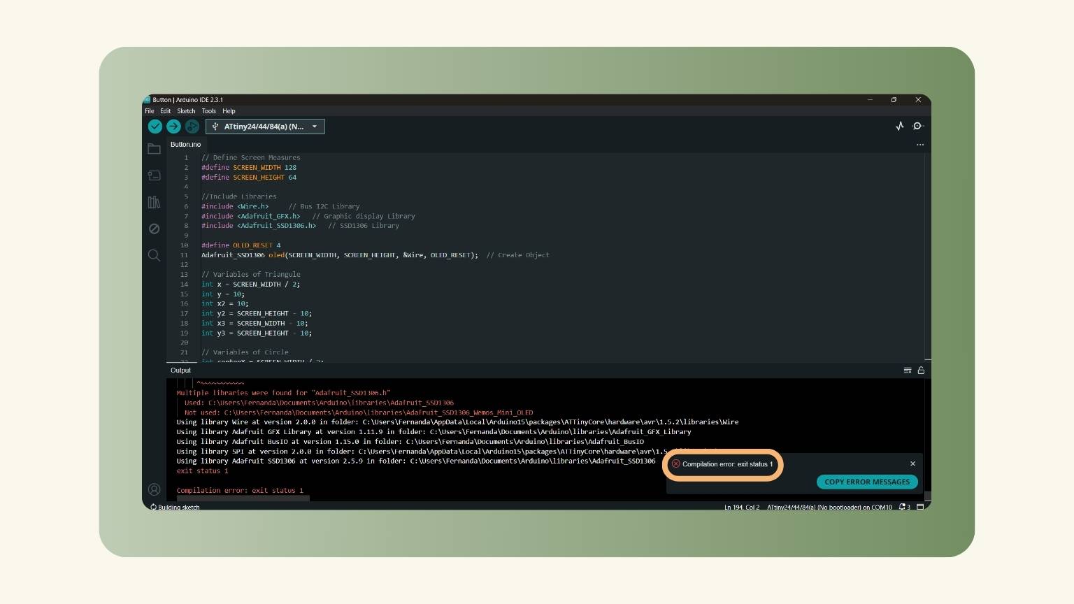
- But then, I had a problem uploading the code of the OLED because it appeared to be an error of ‘Compilation error: exit status 1’.
- So, I verified:
- The programmer in the Tools section.
- That the connections were fine.
- And everything was all right, but the code wasn't uploaded.
Second Try
- I searched for the reason for the above error and found that the library that I used wasn’t compatible with Attiny. So, I found another one to try.
- I tried for three libraries:
- U8g2_for_Adafruit_GFX:It was heavy; the error said, ‘Compilation error: text section exceeds available space exceeds space on board’.
- TinyOzOled:It was the error of 'A programmer is required to upload’'.
- Tiny4kOLED.h:It was again heavy.
Third Try
- I used the TinyOzOled library again.
- So, I burned the bootloader again of the Attiny 44.
- And I used this code:
- Then, I decided to only connect the attiny to udloap the code.
- When the code was uploaded, I connected the OLED to the Attiny.
- But it didn't work.
Fourth Try
- I used the same library and code, but now I used a protoboard to see what the problem was.
- Again, it failed.
After making different tests and trying different things, the result was always the same. Therefore, I would like to further evaluate the following:
- The compatibility of the libraries.
- The connection modes.
- The use of a breadboard.
- Making other boards.
Final Try?
Meanwhile, I decided to give up and use only Arduino Uno for programming.
- So, I used the basic libraries:
- Adafruit GFX Library
- Adafruit SSD1306
- I connected the OLED to the Arduino.
- I used this code:
- I uploaded the code.
- And it worked!
Last Try?
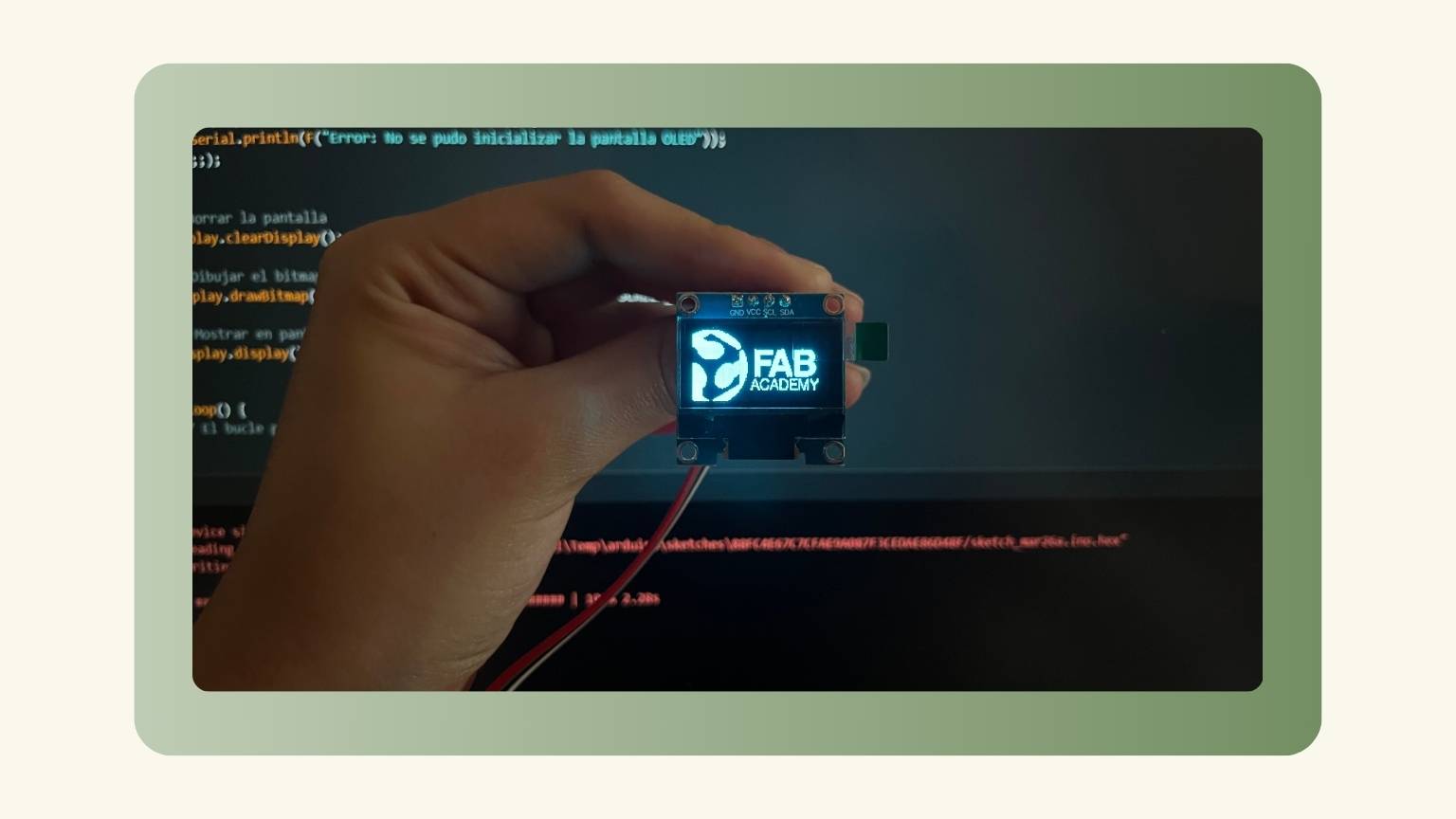
Finally, I used a board that I made, the Quentorres that we made in week 4.
I followed the same steps for the Arduino. I only changed the board to the Xiao and the 'Additional board manager URL'.
And thank God... it worked!
Results
First
I created a code that increases the size of a circle until it reaches the maximum size allowed by the screen. Then, a text appears indicating the color of the circle.
And this is the result:
Second
My second code aimed to display the symbols that inspired my previous PCB design. I wanted to demonstrate the association between colors and shapes. First, I showed the colors represented by the three basic shapes. Then I displayed the color combinations in relation to them.
>And this is the result:
Conclusion
Last week, I thought it was difficult. However, this week has proven to be even more difficult because I didn't know what was going to happen.