As someone I know would say... "a mover ese cuerpo!".
You can see more info about Output Devices in this week's Group Assignment.
A new beginning...
Embarking on the creation of a new PCB for my final project, I drew upon the lessons learned from the previous week's challenges. This time, with the help of my dear professor Javier Osorio Figueroa, I adopted a segmented approach, reminiscent of constructing with Legos, where the main PCB hosts only the Xiao ESP32-C3 along with output pins. These pins serve as conduits for connecting additional PCB modules, allowing for the seamless continuation of signals.
The process began with initial sketches and drawings, aiming to visualize this new direction and forge a stronger understanding of both electronic principles and ergonomic PCB design. These preliminary designs acted as a blueprint, guiding the layout and integration of components in a manner that balanced technical requirements with user interaction.
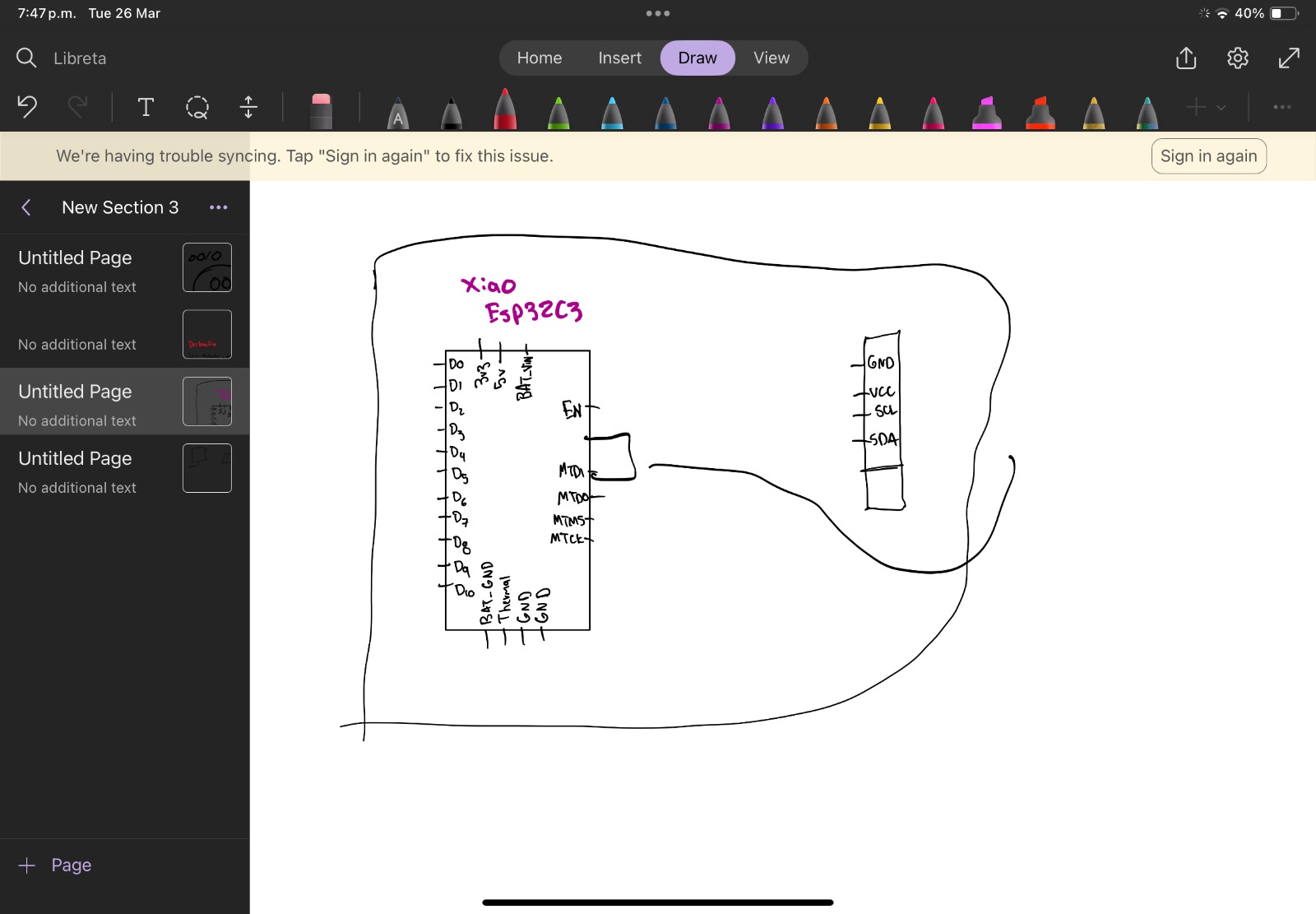
A key consideration in this redesign was the placement of the XIAO module. Ensuring the USB-C connector was positioned at the bottom of the enclosure, reminiscent of a Gameboy, not only catered to aesthetic and functional requirements but also facilitated easy access for programming and power. Above this, the PCB housing the Xiao was designed to accommodate additional buttons, integrating control inputs directly above the microcontroller unit (MCU). This arrangement streamlined the design, emphasizing a compact and user-friendly interface.
Utilizing KiCad and maintaining the component selection from my previous attempt, I pivoted in my design philosophy, focusing on modularity and flexibility.
First, I started a new project but maintaining the main components of my previous design.
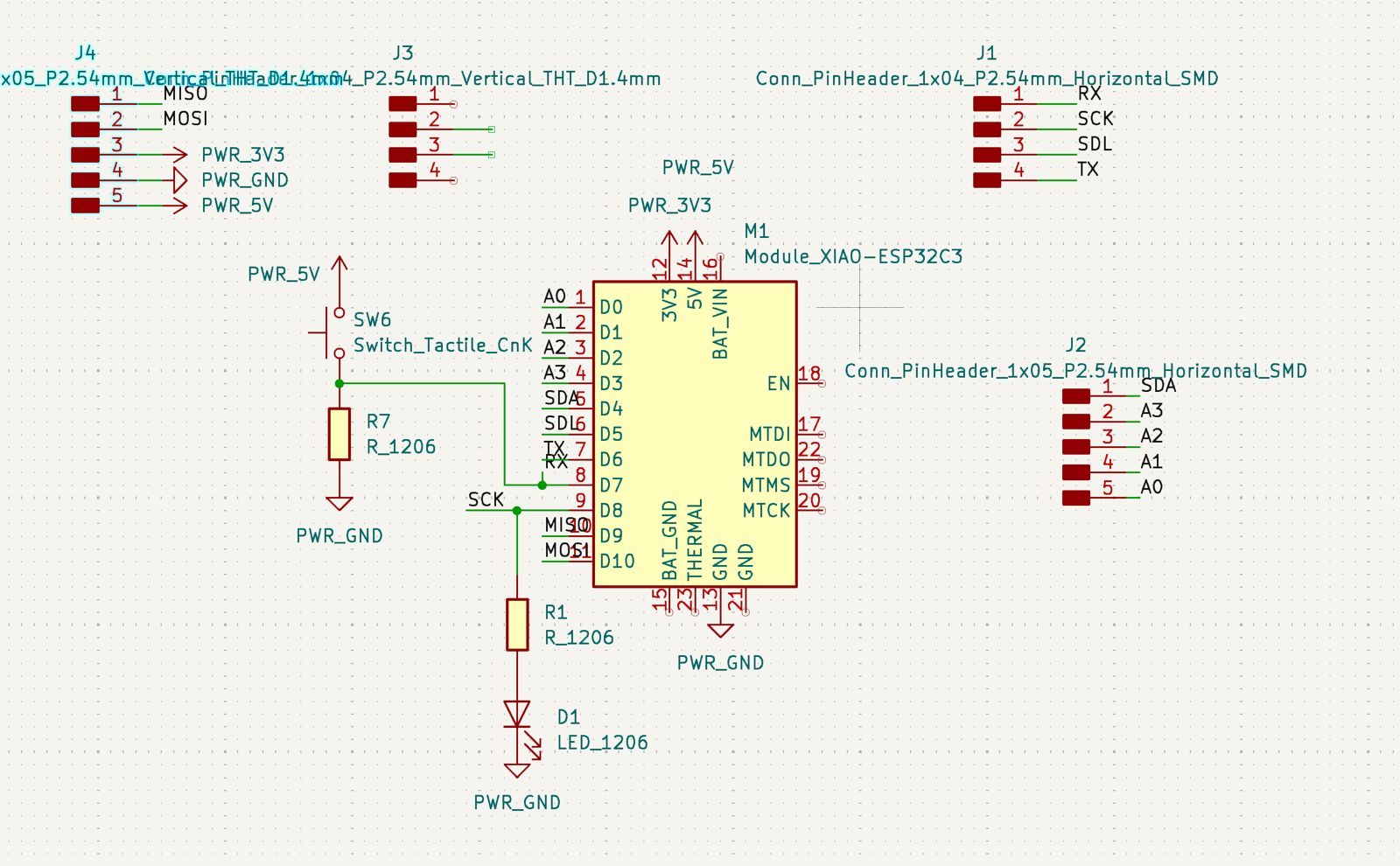
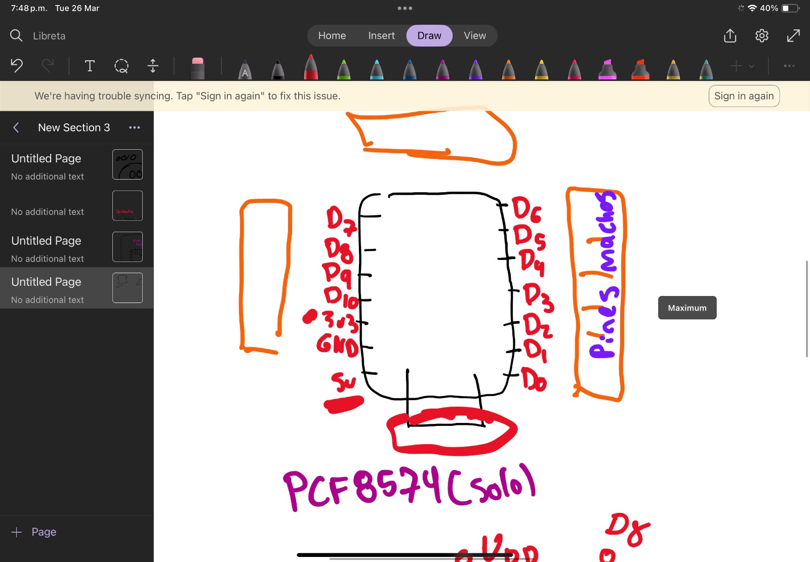
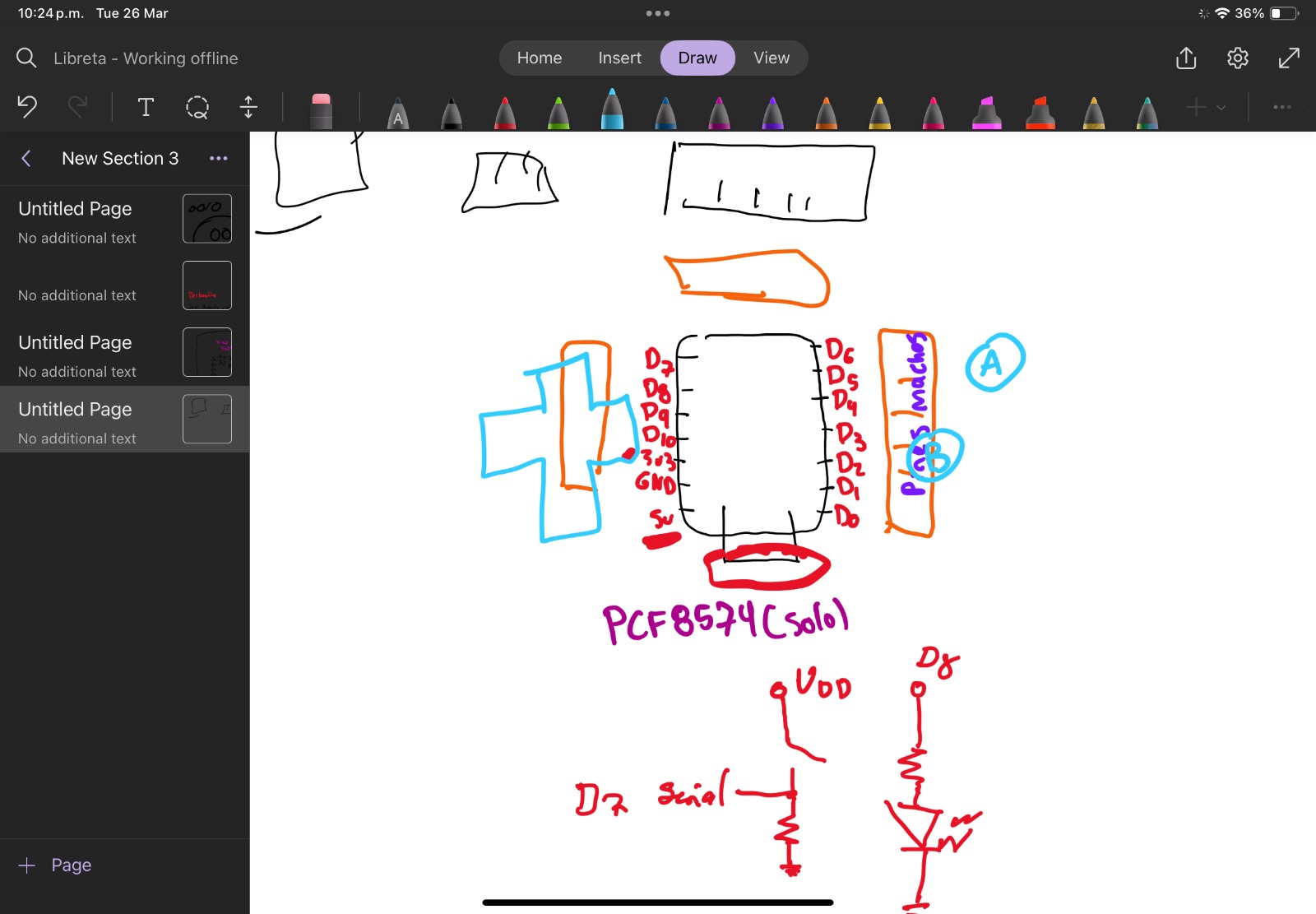
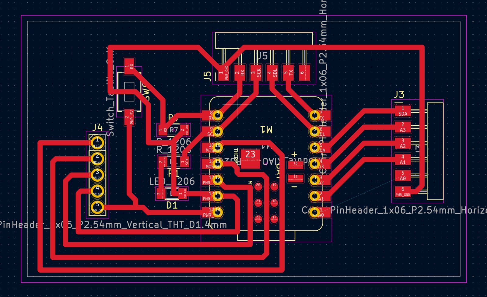
The schematic I’ve created here is an innovation of my previous final project PCB design and now a segment of the GameShine. At the center of this design is the M1, a Module_XIAO-ESP32C3 microcontroller. This little powerhouse is the core of my PCB, equipped with pins for power, ground, analog, and digital signals, as well as communication interfaces like SPI and I2C.
On the sides, I’ve placed connectors J1 through J4. J1 and J2 are SMD connectors; J1 is set up for serial communication with RX and TX pins, and J2 is for I2C communication with SDA and SCL. J3 and J4, with their vertical orientation, are there for SPI communication and power connections. I've used different connectors for different functions, which helps in testing and modular design, as I can easily connect or disconnect parts of my circuit.
Then there’s R1 and R7, both resistors in a 1206 SMD package. Their values aren't specified in this snippet, but their placement in the circuit shows that they will be used for limiting current or setting up pull-up/pull-down resistors, which are essential for stable operation of the inputs and outputs.
The LED, D1, paired with R1, serves as a status indicator. When I power up the board, it should light up, giving me immediate visual feedback that everything’s energized and working as expected. The resistor R1 is there to ensure the LED isn't overdriven, which could lead to it burning out.
SW6, the tactile switch, is a simple input device. By connecting it to PWR_5V and ground through R7, I’m planning for it to serve as a reset button or a user input. It's a straightforward but essential piece of user interface, giving me the ability to interact with the system directly.
This schematic serves as my blueprint. From here, I'll transition to laying out the actual PCB, where I'll place these components according to this design and route the connections between them. It's a crucial step in bringing my electronic design from a concept to a physical object I can hold in my hands and use.
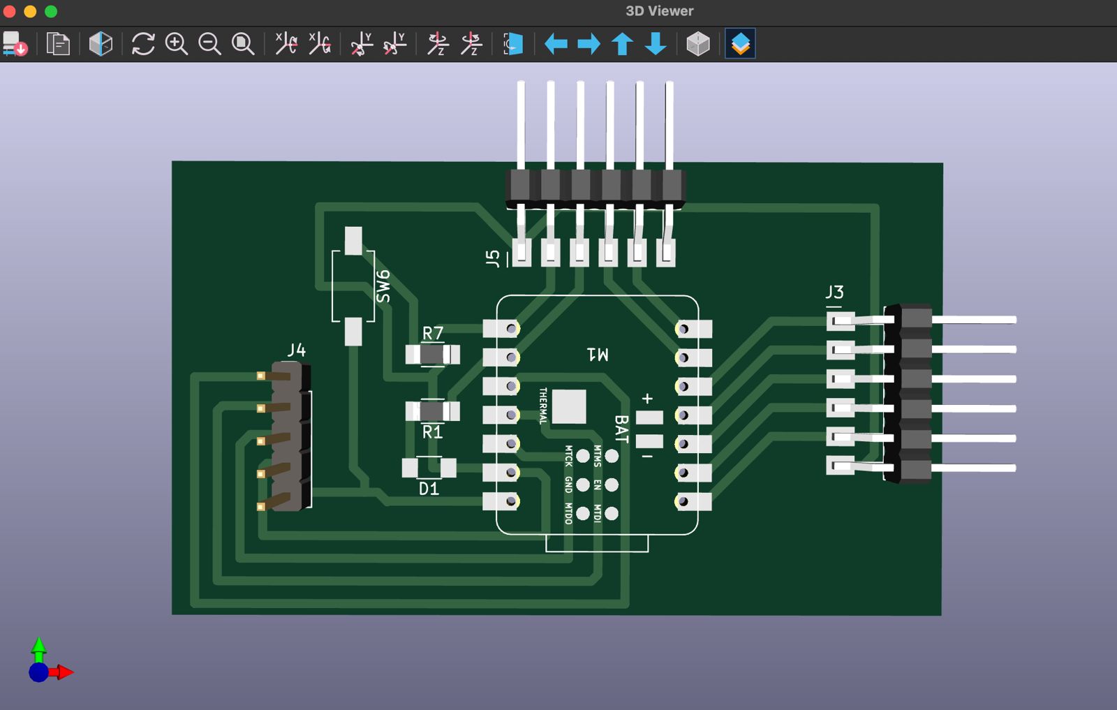
Next, the PCB layout and going once again at the cable puzzle game! Just like the previous week I generated the edge cuts, user drawings and margin so that it is ready to print. For this board I didn't had any problems since the design was relatively simple and it was well designed so that everything fitted together correctly.
Finally, here is a 3D view of how the PCB will look:
Turn up the volume!
What is a game console without it's iconic music?!?!
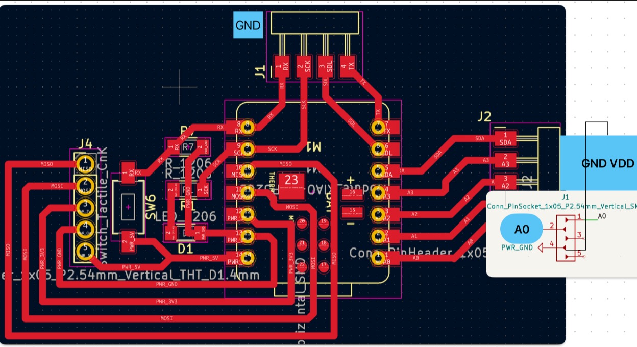
Parallel to the main PCB's development, I embarked on designing a dedicated PCB for an audio output device. To be able to do this I needed to get two signals out of my main PCB. Those being a digital signal which I chose as A0, and PWR_GND. These two signals will enter to the female pins of the new PCB in conjuction with the VDD and GND of the battery.
This new module also included a speaker and was augmented with an integrated LM4871 3W Audio Power Amplifier. Recognizing the importance of sound quality and volume control in my project, I turned to the amplifier's datasheet, which provided a recommended configuration for driving a speaker. This guidance was invaluable, as it offered a tested and effective design for integrating the amplifier, ensuring optimal audio performance from my device.
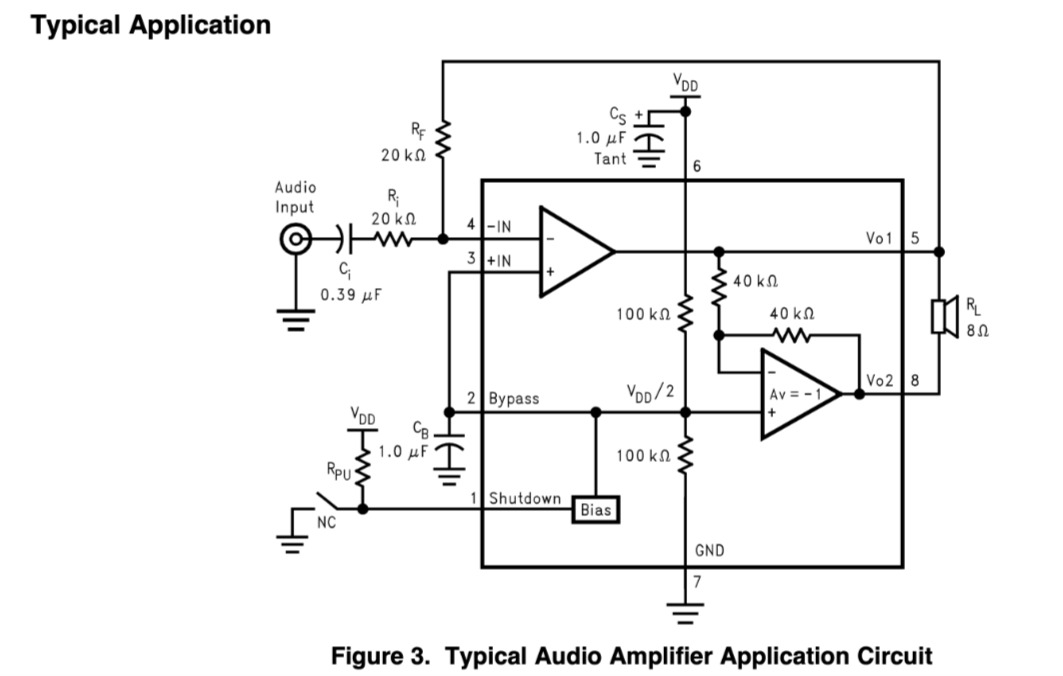
Following the datasheet's recommendations, I carefully crafted the new PCB, incorporating the LM4871 amplifier to drive the speaker efficiently. This meticulous attention to detail was aimed at achieving a high-quality audio output, an aspect crucial for the immersive experience intended with my final project. The process of translating the datasheet's theoretical configuration into a practical PCB layout was both challenging and enlightening, offering deep insights into the nuances of audio electronics.
At the end, things like the Audio Input became my digital A0 signal, I also implemented C_1206 capacitors into the design and a push button for the shutdown option of the integrated amplifier!
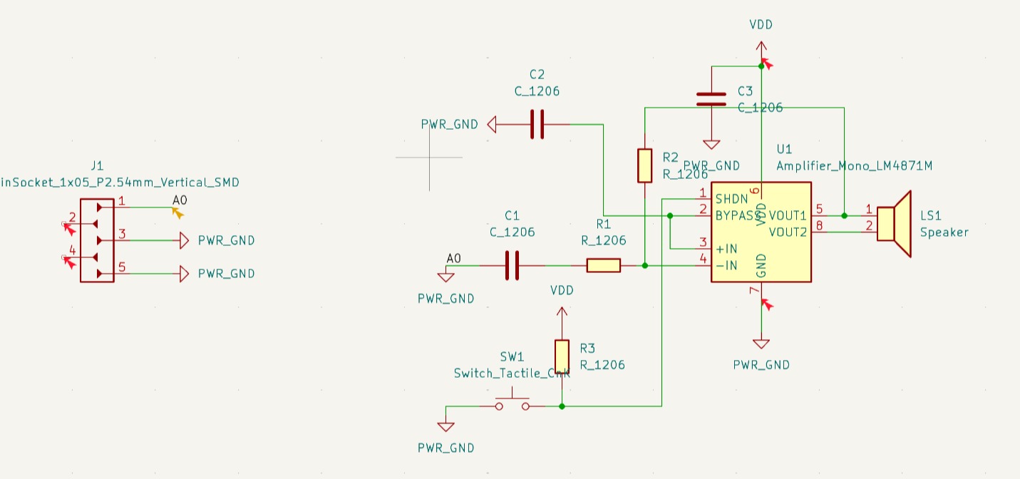
Here I had some errors that were mostly due to my little knowledge with KiCad. These were mostly due to the tags and because the signal of A0 was in conjuction with a PWR_GND signal it made it so in the schematic layout everything was A0! I also didn't know what voltage I would have for the design at this time so I needed to add a VDD signal to the female pins.
Once I replicated the recommended configuration from the datasheet, I proceeded to make the PCB layout.
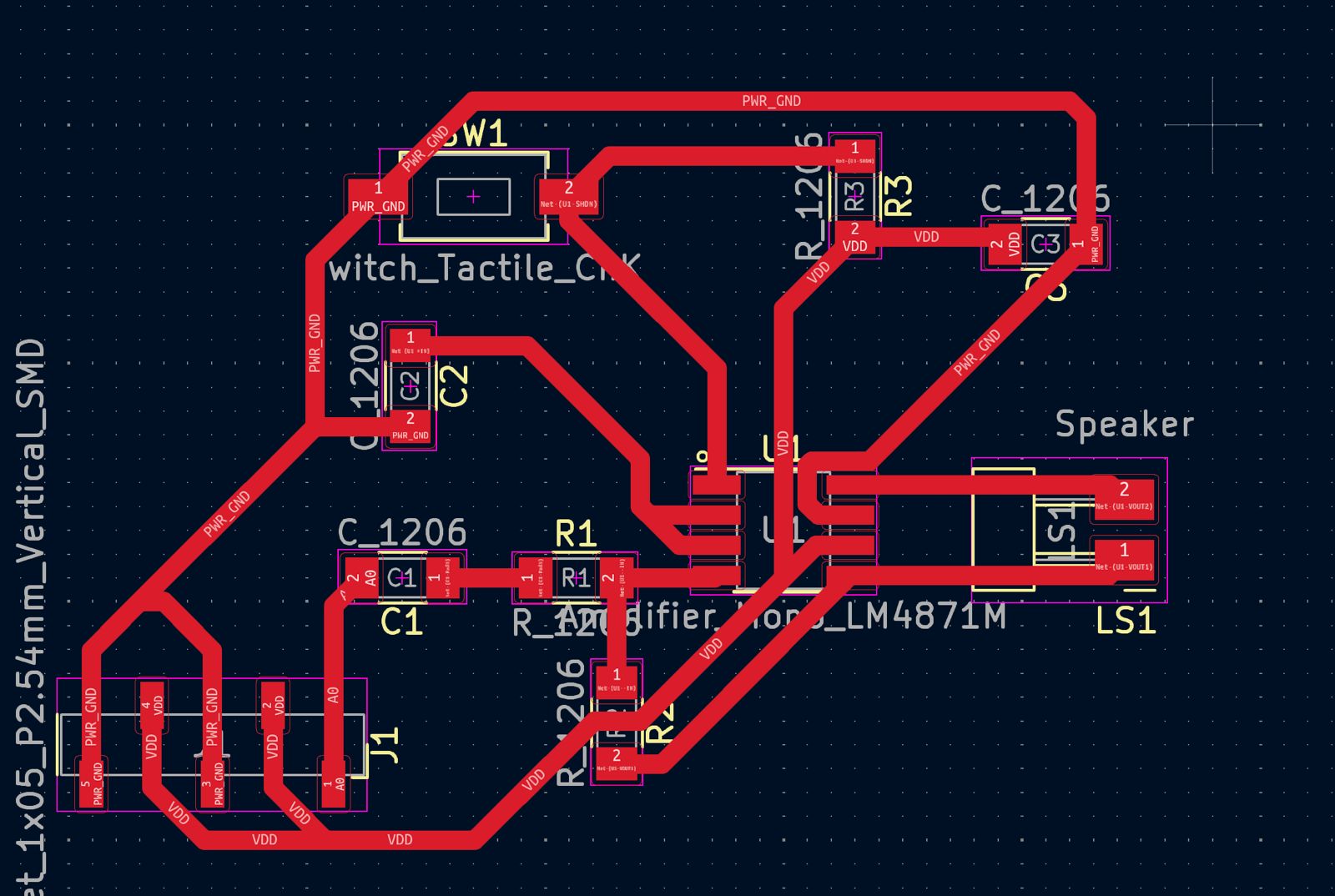
And here is a 3D view of how it would look! Just keep in mind that KiCad couldn't render certain components so that is why somethings like the speaker look... weird
.jpeg)
Now all that is left is just to get them produced and get all the pieces... and that would be really easy if we weren't in the middle of a spring break lol.
Mexican Spring Break!
Progress on this ambitious endeavor has temporarily stalled. Currently, Mexico is in the midst of spring break, introducing unexpected limitations that have impacted my project timeline (AGAIN LOL). The holiday season has led to the temporary closure of facilities essential for PCB fabrication, alongside the storages housing necessary integrated circuits. This pause has been a reminder of the importance of external factors in project planning and execution.
Despite these setbacks, the journey of interfacing output devices with a microcontroller has been a profoundly educational experience. Learning to control devices, such as speakers through amplifiers, has deepened my understanding of electronic circuits and their interaction with programmable logic. This exploration into output devices has underscored the versatility and power of microcontrollers, highlighting their capability to bring a wide array of functionalities to life, from sound to digital interfaces.
Update: 05/20/2024
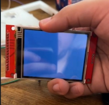
I decided to change my Output Devices and rather than focus on the speaker I decided to focus on the ILI9341 Display.
In my GameShine project, the focus is on integrating and utilizing ILI9341 displays to enhance the user interface and overall functionality of the device.
Connecting the ILI9341 DisplayConnecting the ILI9341 display involves establishing connections for power, ground, data, and control lines. Here is a general outline of the necessary connections:
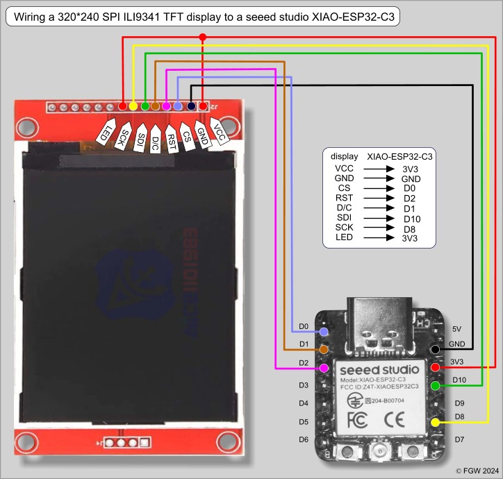
- Power (VCC): Connect the VCC pin to a 3.3V or 5V power source, depending on the specifications of your ILI9341 display.
- Ground (GND): Connect the GND pin to the ground of your power source to complete the circuit.
- MOSI (Master Out Slave In): Connect this to the SPI MOSI pin on your microcontroller.
- SCK (Serial Clock): Connect this to the SPI SCK pin on your microcontroller.
- CS (Chip Select): Connect this to a digital pin on your microcontroller to enable or disable the SPI communication.
- DC/RS (Data/Command): Connect this to another digital pin to switch between data and command modes.
- RST (Reset): Connect this to a reset pin or a digital pin on your microcontroller to reset the display.
- LED (Backlight): Connect this to a power source or control it via a PWM pin for adjustable brightness.
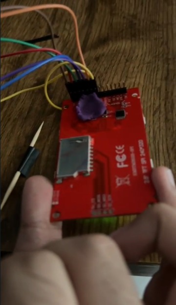
One of the main issues encountered with the ILI9341 display was the backlight not functioning correctly. Several factors could cause this problem, including incorrect wiring, insufficient power supply, or a fault in the display module itself. Ensuring that the backlight pin (often labeled LED) is connected to the appropriate power source or control pin is crucial.
After thorough troubleshooting, I determined that the backlight issue was due to a defective display module. To continue working on my project while waiting for a replacement, I implemented a creative temporary fix. I added play-doh into the display. This unconventional solution allowed me to maintain some functionality and continue development and testing without significant delays.
Once the replacement display arrived, I replaced the faulty module, ensuring the backlight functioned correctly and the display operated as expected.
Despite these setbacks, the journey of interfacing output devices with a microcontroller has been a profoundly educational experience. Learning to control devices, such as speakers through amplifiers, has deepened my understanding of electronic circuits and their interaction with programmable logic. This exploration into output devices has underscored the versatility and power of microcontrollers, highlighting their capability to bring a wide array of functionalities to life, from sound to digital interfaces.
Using the ILI9341 Adafruit Library and Adafruit_GFXTo test the display, I utilized the Adafruit ILI9341 library. This library simplifies interfacing with the ILI9341 display and provides a range of functions for control. Here’s how I used the library effectively:
- Library Installation: I installed the Adafruit ILI9341 library via the Arduino Library Manager. Additionally, I installed the Adafruit GFX library, which provides essential graphics functions.
- Testing the Display: I loaded an example sketch from the Adafruit ILI9341 library. I adjusted the pin definitions in the sketch to match my specific wiring setup. I then uploaded the sketch to my microcontroller and observed the display to ensure it functioned correctly.
Example sketch:
The example code provided demonstrates the use of the Adafruit ILI9341 library to interface with the ILI9341 display. Here’s a detailed explanation of the code:
- Library Inclusions: The code includes the SPI, Adafruit_GFX, and Adafruit_ILI9341 libraries, which are necessary for SPI communication and graphics operations.
- Pin Definitions: The code defines the pins used for SPI communication and display control.
- Display Object Initialization: An Adafruit_ILI9341 object is created using the defined pins.
- Setup Function: This function initializes serial communication, resets the display, begins the display, and reads diagnostic information.
- Loop Function: This function rotates the display and tests text rendering.
- Benchmark Functions: These functions test various display operations and measure the time taken for each operation.
#include "SPI.h"
#include "Adafruit_GFX.h"
#include "Adafruit_ILI9341.h"
#define TFT_DC D1
#define TFT_CS D0
#define TFT_RST D2
Adafruit_ILI9341 tft = Adafruit_ILI9341(TFT_CS, TFT_DC);
void setup() {
	Serial.begin(9600);
	Serial.println("ILI9341 Test!");
	pinMode(TFT_RST, OUTPUT);
	digitalWrite(TFT_RST, LOW);
	delay(50);
	digitalWrite(TFT_RST, HIGH);

	tft.begin();

	uint8_t x = tft.readcommand8(ILI9341_RDMODE);
	Serial.print("Display Power Mode: 0x"); Serial.println(x, HEX);
	x = tft.readcommand8(ILI9341_RDMADCTL);
	Serial.print("MADCTL Mode: 0x"); Serial.println(x, HEX);
	x = tft.readcommand8(ILI9341_RDPIXFMT);
	Serial.print("Pixel Format: 0x"); Serial.println(x, HEX);
	x = tft.readcommand8(ILI9341_RDIMGFMT);
	Serial.print("Image Format: 0x"); Serial.println(x, HEX);
	x = tft.readcommand8(ILI9341_RDSELFDIAG);
	Serial.print("Self Diagnostic: 0x"); Serial.println(x, HEX);

	Serial.println(F("Benchmark                Time (microseconds)"));
	delay(10);
	Serial.print(F("Screen fill              "));
	Serial.println(testFillScreen());
	delay(500);

	Serial.print(F("Text                     "));
	Serial.println(testText());
	delay(3000);

	Serial.print(F("Lines                    "));
	Serial.println(testLines(ILI9341_CYAN));
	delay(500);

	Serial.print(F("Horiz/Vert Lines         "));
	Serial.println(testFastLines(ILI9341_RED, ILI9341_BLUE));
	delay(500);

	Serial.print(F("Rectangles (outline)     "));
	Serial.println(testRects(ILI9341_GREEN));
	delay(500);

	Serial.print(F("Rectangles (filled)      "));
	Serial.println(testFilledRects(ILI9341_YELLOW, ILI9341_MAGENTA));
	delay(500);

	Serial.print(F("Circles (filled)         "));
	Serial.println(testFilledCircles(10, ILI9341_MAGENTA));

	Serial.print(F("Circles (outline)        "));
	Serial.println(testCircles(10, ILI9341_WHITE));
	delay(500);

	Serial.print(F("Triangles (outline)      "));
	Serial.println(testTriangles());
	delay(500);

	Serial.print(F("Triangles (filled)       "));
	Serial.println(testFilledTriangles());
	delay(500);

	Serial.print(F("Rounded rects (outline)  "));
	Serial.println(testRoundRects());
	delay(500);

	Serial.print(F("Rounded rects (filled)   "));
	Serial.println(testFilledRoundRects());
	delay(500);

	Serial.println(F("Done!"));
	}
void loop(void) {
	for(uint8_t rotation=0; rotation4; rotation++) {
		tft.setRotation(rotation);
		testText();
		delay(1000);
	}
	}
unsigned long testFillScreen()
unsigned long testText()
unsigned long testLines(uint16_t color)
unsigned long testFastLines(uint16_t color1, uint16_t color2)
unsigned long testFilledRects(uint16_t color1, uint16_t color2)
unsigned long testFilledCircles(uint8_t radius, uint16_t color)
unsigned long testCircles(uint8_t radius, uint16_t color)
unsigned long testTriangles()
...
The code in action:
Creating a custom boot-up screen for my GameShine project involved designing the screen layout and programming it using the Adafruit ILI9341 library. Here are the detailed steps I followed:
- Design: Inspired in the GameBoy startup screen.
- Code Implementation: In my setup code, I initialized the display using the functions provided by the Adafruit ILI9341 library. I utilized the drawBitmap function or other graphics functions from the Adafruit GFX library to render the boot-up screen image on the display. I made sure that the backlight was correctly initialized and controlled to display the screen properly.
This code is the GameShine startup screen using the ILI9341 display. It includes the setup and implementation of a boot-up screen and game selection menu. Below are the key parts of the code:
Libraries and Pin Definitions: The Adafruit GFX and ILI9341 libraries are included for graphical functions and controlling the display. Define pins for chip select (TFT_CS), reset (TFT_RST), and data/command (TFT_DC) for the ILI9341 display.
#include
#include
#include

#define TFT_CS    D0
#define TFT_RST   D2
#define TFT_DC    D1

Adafruit_ILI9341 tft = Adafruit_ILI9341(TFT_CS, TFT_DC, TFT_RST);

#define pin_up A5
#define pin_down A3
Splash Screen and Menu Functions:
void splashScreen() {
	tft.fillScreen(ILI9341_BLACK);

	// Draw "GAMESHINE" logo with pulsing animation
	static float textSize = 3.0;
	static bool increasing = true;
	const float textSizeMin = 2.5;
	const float textSizeMax = 3.5;
	const float textSizeStep = 0.05;

	if (increasing) {
		textSize += textSizeStep;
		if (textSize > textSizeMax) increasing = false;
	} else {
		textSize -= textSizeStep;
		if (textSize < textSizeMin) increasing = true;
	}

	const char *title = "GAMESHINE";
	const char *subtitle = "A Fab Academy Project";

	// Center text calculations
	int16_t x1, y1;
	uint16_t w, h;

	// Calculate center for title
	tft.setTextSize(textSize);
	tft.getTextBounds(title, 0, 0, &x1, &y1, &w, &h);
	int16_t x = (310 - w) / 2 + 10;
	int16_t y = (320 - h) / 2 - 60 ;

	tft.setCursor(x, y);
	tft.setTextColor(ILI9341_RED);
	tft.println(title);

	// Calculate center for subtitle
	tft.setTextSize(2);
	tft.getTextBounds(subtitle, 0, 0, &x1, &y1, &w, &h);
	x = (310 - w) / 2 + 10;
	y = (320 - h) / 2 - 35;

	tft.setCursor(x, y);
	tft.setTextColor(ILI9341_WHITE);
	tft.println(subtitle);
	}

	void menu() {
	tft.fillScreen(ILI9341_BLACK);

		// Draw hexagons
	for (int i = 0; i < 50; i++) {
		int x = rand() % 240;
		int y = rand() % 320;
		int size = rand() % 20 + 10;
		uint16_t color = rand() % 65536;
		drawHexagon(x, y, size, color);
	}

	// Animate the "GAMESHINE" logo
	static uint8_t colorIndex = 0;
	uint16_t colors[] =  { ILI9341_RED, ILI9341_GREEN, ILI9341_BLUE, ILI9341_YELLOW, ILI9341_CYAN };
	tft.setCursor(30, 50);
	tft.setTextColor(colors[colorIndex]);
	tft.setTextSize(3);
	tft.println("GAMESHINE");

	tft.setCursor(50, 150);
	tft.setTextColor(ILI9341_GREEN);
	tft.setTextSize(2);
	tft.println("1. Space Trash");
	tft.setCursor(50, 200);
	tft.setTextColor(ILI9341_BLUE);
	tft.println("2. GalaFab");

	// Update color index
	colorIndex = (colorIndex + 1) % 5;
	}
- Splash Screen: Displays the "GAMESHINE" logo with a pulsing animation and a subtitle "A Fab Academy Project."
- Menu: Displays a menu with two game options ("Space Trash" and "GalaFab") and hexagon decorations. The logo color cycles through different colors.
Setup and Main Loop
void setup() {
	tft.begin();
	tft.setRotation(1);
	tft.fillScreen(ILI9341_BLACK);
	}

	unsigned long startTime;
	bool splashScreenDone = false;
	uint8_t gameSelection = 0;

	void loop() {
	if (!splashScreenDone) {
		unsigned long currentTime = millis();
		if (currentTime - startTime > 15000) { // Show splash screen for 15 seconds
		splashScreenDone = true;
		} else {
		splashScreen();
		}
	} else {
		static unsigned long lastUpdate = 0;
		if (millis() - lastUpdate > 500) { // Update every 500 milliseconds
		menu();
		lastUpdate = millis();
		}

		if (gameSelection == 0) {
		if (digitalRead(pin_up)) {
			gameSelection = 1;
			delay(200);
		} else if (digitalRead(pin_down)) {
			gameSelection = 2;
			delay(200);
		}
		}

		if (gameSelection == 1) {
		st_Setup();
		for (;;) {
			static uint8_t direction = 0; // 0 for down, 1 for up
			st_Step(y, 1, 1); // Automatic fire enabled

			if (direction == 0) {
			y++;
			if (y >= 255) {
				direction = 1;
			}
			} else {
			y--;
			if (y <= 1) {
				direction = 0;
			}
			}

			tft.fillScreen(ILI9341_BLACK);
			st_Draw(0);
		}
		} else if (gameSelection == 2) {

		// To be implemented...
		}
	}
	}
- Setup Function: Initializes the display and fills the screen with black.
- Main Loop:
- Displays the splash screen for 15 seconds.
- Then shows the menu, updating every 500 milliseconds.
- Waits for user input to select a game.
- Starts the "Space Trash" game if selected.
- Or starts the "GalaFab" game if selected.
- Game Functions:
- st_Step: Handles game states and transitions between splash screen, menu, and game states.
- st_Draw: Draws the game elements on the screen based on the current state.
- st_Setup: Initializes game elements.
By organizing these functions and handling transitions smoothly, the code creates a cohesive boot-up experience for the GameShine.
Here is a video of the startup screen in action:
Conclusion:
In conclusion, while the current break has momentarily halted physical progress, the conceptual and design phases have advanced significantly. This period has allowed me to refine my approach, focusing on modular design and the integration of output devices. The challenges encountered have not only tested my resilience but have also enriched my knowledge, setting a solid foundation for future endeavors. As I await the resumption of normal operations, my project stands poised for rapid progression, backed by a deeper understanding of electronics and a renewed appreciation for the intricacies of PCB design.
This pause, though frustrating, has offered an unexpected opportunity to reflect and learn, reinforcing the importance of adaptability and persistence in the face of unforeseen challenges. As I look forward to resuming my work, the experiences of the past weeks serve as a testament to the complexity and reward of electronic design, a journey marked by continuous learning and the joy of creation.
After the pause, I decided to focus on better working on the heart of the project. This project integrates an ILI9341 display to create an engaging boot-up experience for the GameShine project. The setup involves connecting the display to a microcontroller and utilizing the Adafruit ILI9341 library for control and graphical output. The code showcases key functionalities, including a splash screen with pulsing animations, a dynamic menu, and a basic game framework. Through careful structuring and detailed implementation, this setup not only enhances the visual appeal but also provides a smooth user interface, setting a solid foundation for future developments in the GameShine project. By addressing initial hardware issues creatively and leveraging robust libraries, the project demonstrates a blend of technical troubleshooting and design, ensuring an immersive and professional user experience.
The Files:
Below you can find the download links for all of the files from this week.
New Main PCB files:
Speaker PCB files:
- {GamingPCB2-F_Cu.svg}
- {GamingPCB2-User_Drawings.svg}
- {GamingPCB2 mill traces}
- {GamingPCB2 mill outline}