Murphy's Law: "Anything that can go wrong will go wrong".
An Apology
I'd like to extend a heartfelt apology as I reflect on this week's assignment.
It was a testament to Murphy's Law, an axiom we've all heard and humorously applied, but this time, it held true with a weight that was anything but light-hearted.
Tasked with fabricating a PCB at the Fab Lab Puebla, I grappled not only with the design intricacies but also with the sheer logistical challenge of accessing a solitary CNC machine among a cohort of eager students. The air was thick with anticipation and anxiety as each of us awaited our turn, and the clock ticked on without mercy. The strain was palpable; each setback felt like a blow to my plans. The experience, although fraught with stress, was enlightening—a true test of a strong mind and the acceptance of failure.
So to my local and global evaluator, and especially Neil, I would like to say that I am sorry. I recognize the gap in my delivery and am committed to dedicating my personal time to rectify the situation. I’m looking forward to demonstrating the work I intended to deliver and appreciate your understanding.
With that said, here is the rest of my documentation...
Let me take you through the basics!
This week commenced with an essential grounding in electronics, equipping us with the knowledge needed for circuit design. We compared SMT (Surface Mount Technology) and THT (Through-hole Technology), opting to use SMT for its suitability to our project scope. For creating traces, while finer parameters are viable for professional manufacturing, we adopted broader measurements to facilitate manual assembly.
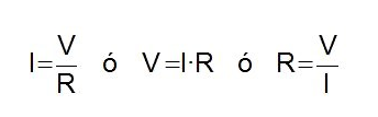
We delved into applying Ohm's Law, a fundamental principle in electronics that correlates current, voltage, and resistance within a circuit. Understanding this law is crucial as it guides the design and functionality of our circuits.
Here are the formulas for Ohm's Law where I is the intensity that is measured in amperes (A), V is the voltage that is measured in volts (V); and R is the resistance that is measured in ohms (Ω).
Our journey into electronics design further delved into the language of circuitry through the study of basic electronic symbology.
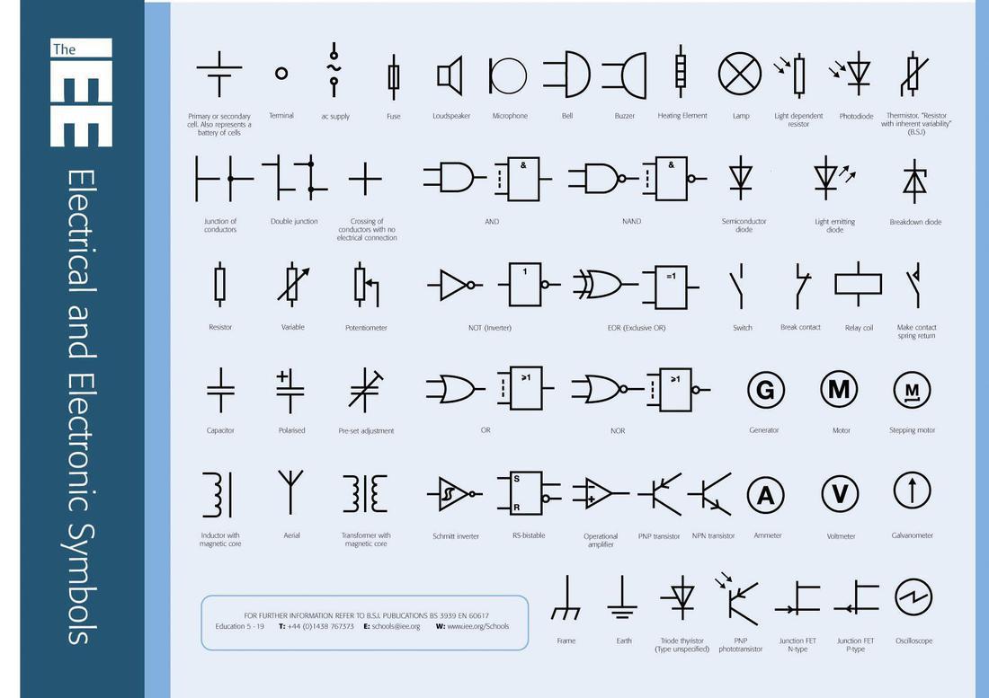
Understanding these symbols is crucial—they are the shorthand that communicates the components and connections within a circuit, bridging the gap between idea and actualization.
Moreover, we embraced the power of KiCad, an open-source software suite for electronic design automation (EDA). KiCad became our drafting board, allowing us to translate the symbols into precise, orderly schematics, and from there into physical board layouts ready for fabrication.
The hands-on experience with KiCad was particularly enlightening, offering a tangible sense of the design process from start to finish.
Testing Testing... is this thing on?!?!
Our excursion to the electronics lab was a hands-on reinforcement of our theoretical knowledge. We began by testing our very own PCB, designed during Week 04.
With the initial step of programming, we introduced the electronic 'Hello World': a LED blink sequence from the initial code we used during that week. Once programmed, the oscilloscope came into play.
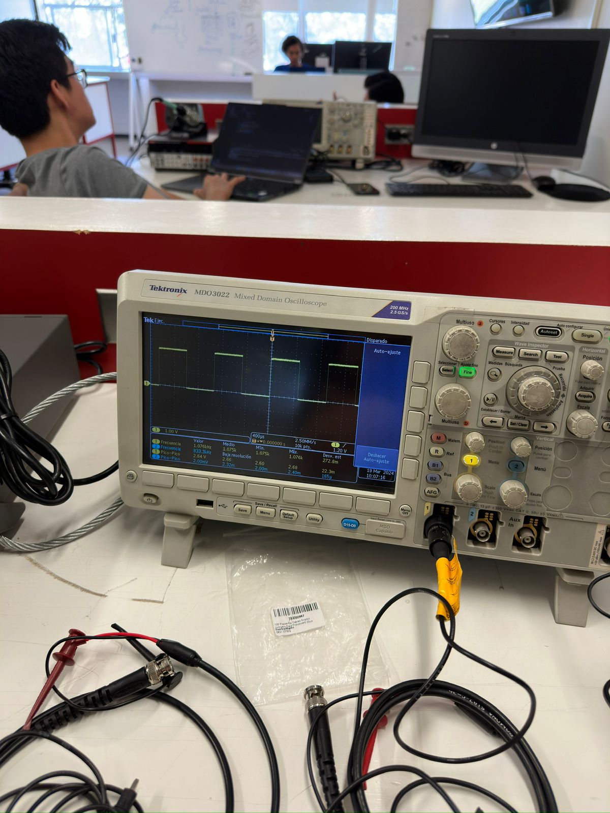
Carefully, we connected the probes and tweaked the settings to capture the LED's digital signals. Observing the distinct square wave patterns on the oscilloscope's screen was a practical lesson in digital electronics.
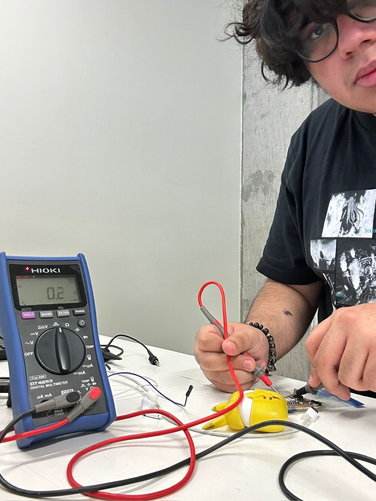
The multimeter was next, a tool just as crucial as the oscilloscope. We measured the current, voltage, and checked for continuity, essential diagnostics for any PCB.
Throughout these exercises, we learned that the values we see are not absolute; they exist within ranges defined by lower and upper limits. This experience wasn't just about measuring and testing; it was a pivotal moment of applying classroom concepts to tangible technology.
You can see more info in this week's Group Assignment.
The PCB
What is KiCad?
KiCad is a free, open-source software suite used for electronic design automation (EDA). It is popular among hobbyists, engineers, and professionals for designing schematics and printed circuit board (PCB) layouts. KiCad offers a comprehensive set of tools to take a project from the initial schematic to a fully realized PCB.
KiCad has various features such as:
- Schematic Capture:
- Symbol Libraries: KiCad comes with extensive symbol libraries, and users can create custom symbols.
- Hierarchical Design: Supports complex hierarchical schematics, enabling the design of multi-sheet projects.
- Electrical Rules Checker (ERC): Ensures that the schematic adheres to standard electrical rules.
- PCB Layout:
- Footprint Libraries: Offers a vast collection of footprints for various components, with the ability to create custom footprints.
- Design Rule Checker (DRC): Verifies that the PCB layout complies with manufacturing constraints.
- Interactive Router: Provides advanced routing features, including push-and-shove and length tuning for high-speed designs.
- 3D Viewer: Visualizes the PCB in 3D, helping to check the placement and appearance of components.
- Footprint Editor:
- Allows users to create and modify footprints, ensuring that each component fits precisely on the PCB.
- Gerber File Generation:
- Exports standard Gerber files used by PCB manufacturers, ensuring compatibility and ease of production.
- Bill of Materials (BOM):
- Generates a detailed BOM, listing all components required for the project, which is essential for procurement and assembly.
- Plugins, Scripting and Libraries:
- Supports Python scripting, various plugins and libraries, extending the functionality of the software.
The process of PCB design begins with drafting the schematic, which outlines the circuit's logic through symbol representations of the components and their connections. Once the schematic is complete, detailing what components are used and how they're interconnected, the focus shifts to creating the PCB layout. This layout translates the schematic into physical paths that electrically connect components on the board itself, forming the backbone of the circuit's functionality. For a more detailed workflow please look at the following step by step guide:
- Schematic Design:
- Start by drafting the schematic, where each component and its connections are defined.
- Use KiCad’s symbol libraries or create custom symbols as needed.
- Perform an ERC to ensure the schematic is free of errors.
- PCB Layout:
- Transfer the schematic to the PCB layout tool.
- Place components on the board, optimizing for space and functionality.
- Route the connections between components, adhering to design rules.
- Use the 3D viewer to inspect the board and ensure the layout meets design requirements.
- Verification and Output:
- Run a DRC to verify that the PCB design adheres to the specified rules.
- Generate Gerber files and a BOM for manufacturing.
- Optionally, create assembly drawings and other documentation.
KiCad also possesses a strong community and support in which they offer extensive documentation, including tutorials and user manuals, making it accessible for beginners. These resources help new users quickly get up to speed with the software. An active community of users and developers contributes to forums, mailing lists, and social media, providing support and sharing knowledge. This vibrant community ensures that users can find help and inspiration for their projects. Continuous development and updates are made by a dedicated team, ensuring KiCad evolves with new features and improvements. Regular updates address bugs, introduce new functionalities, and enhance the user experience.
KiCad's popularity stems from its cost-effectiveness, as it is an open-source tool that is free to use. This makes it accessible to a wide range of users, from hobbyists and students to professionals, without the financial burden of expensive licenses. Despite being free, KiCad offers a comprehensive set of tools that rival those found in commercial EDA software. Its robust feature set, including schematic capture, PCB layout, 3D viewer, and footprint editor, caters to both simple and complex projects.
Additionally, the flexibility and customizability of KiCad are significant factors in its popularity. Users can create custom symbols and footprints, and the software supports Python scripting and various plugins to extend its functionality. The active community and continuous development ensure that KiCad remains up-to-date with the latest advancements in electronic design, making it a reliable choice for designing complex electronic systems from start to finish. Whether you are working on simple circuits or intricate multi-layer boards, KiCad provides the tools and flexibility needed to bring your electronic projects to life.
Getting started with KiCad!
This week's assignment consisted in the design and production of a PCB. However, I wanted to make some advancements on my final project so I decided to use this week to generate the PCB for my game controller, similar to the one from the bottom half of this original Gameboy board.
.jpg)
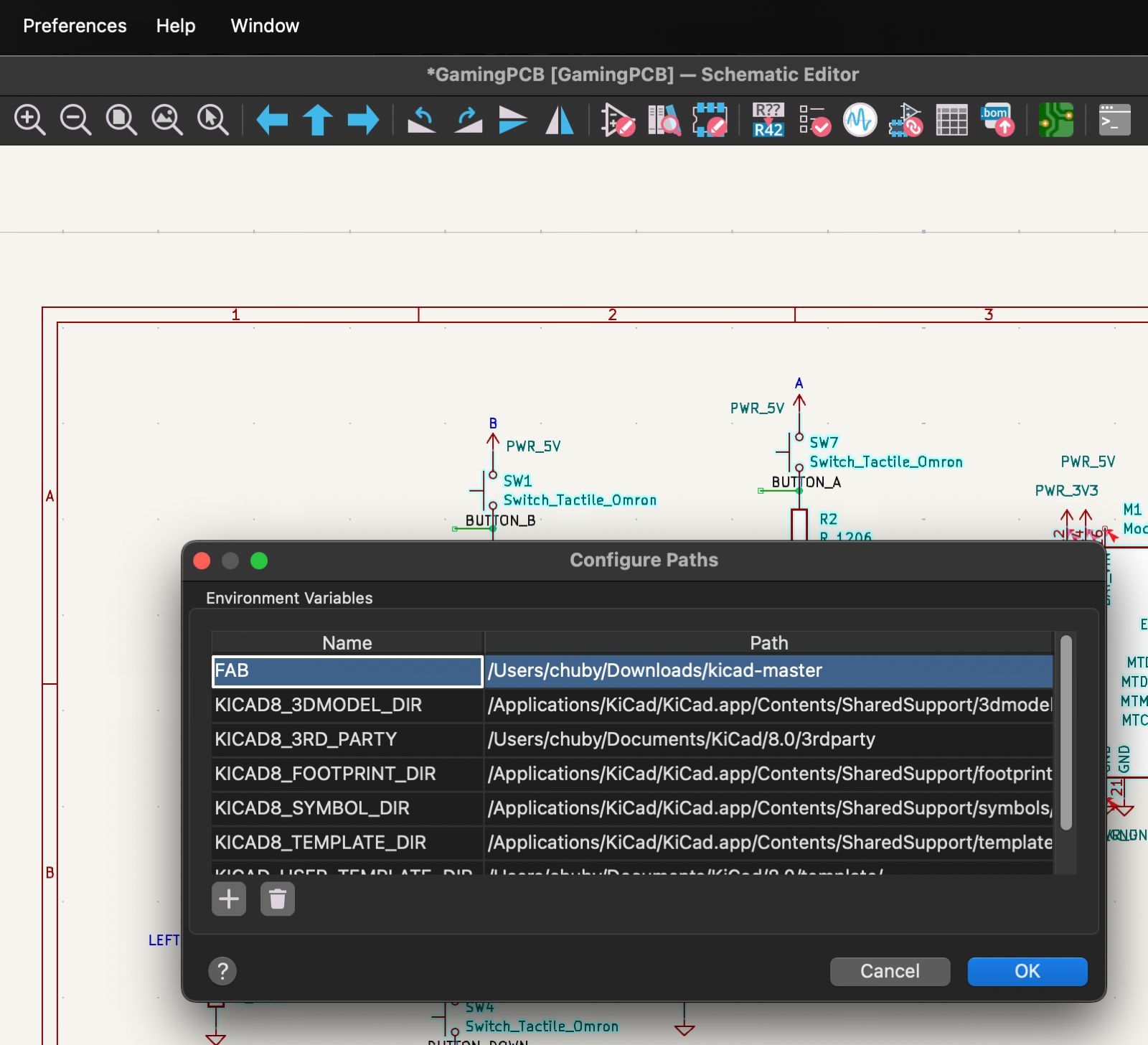
KiCad's robust library system and intuitive interface made it a natural choice for this endeavor, offering all the tools needed for a meticulous yet creative design process. Furthermore, we had a pre-made library that was made specifically for FabLab Puebla that contained every component that we had available at the lab. You can find this library in the following Link.
In order to add a library to KiCad, please follow the next steps:
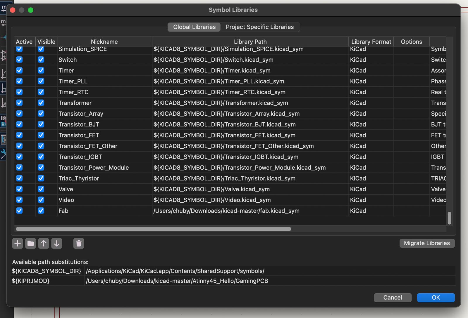
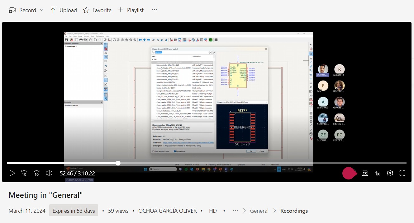
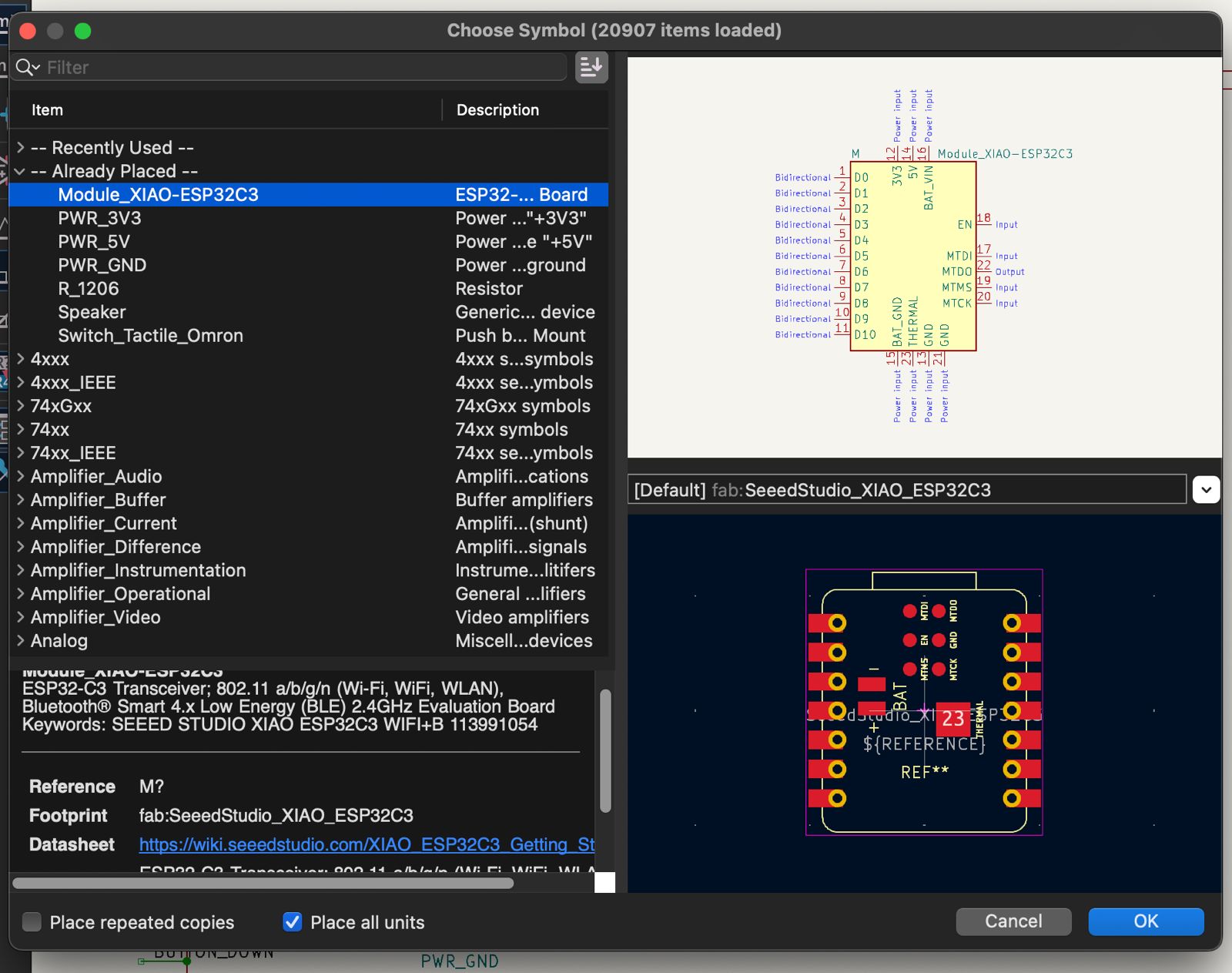
In order to check that the library was installed correctly go to the option of "Add Symbols" that is located on the right-side toolbar. Once it is opened you can type "fab" and it will show every component that is tagged with that word.
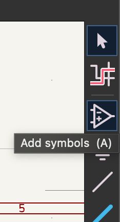
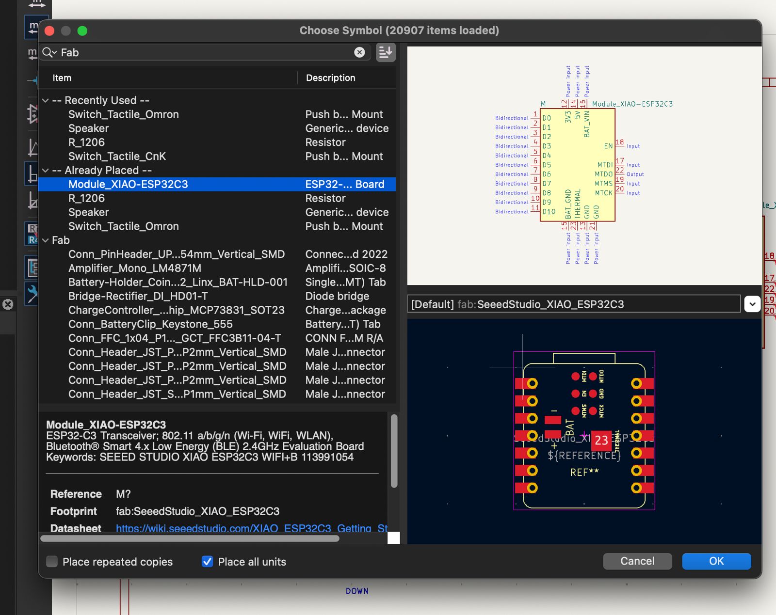
"Add Symbols" refers to the process of placing electronic component symbols into your schematic to represent the various parts of your circuit. These symbols are the building blocks of your circuit design, visually depicting resistors, capacitors, microcontrollers, and more.
You can also do this by checking the "Power Symbol" that is also located on the right-side tooblar.
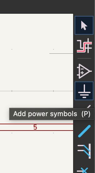
"Power Symbols", on the other hand, are specific symbols used to denote power sources and grounds in the circuit. They help in easily identifying how power is distributed throughout the design, ensuring that all components are correctly powered.
Some more shortcuts include:
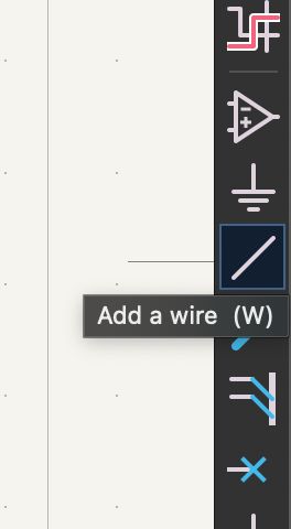
- "Add a Wire (W)" is a shortcut used to connect components within the schematic. This tool allows you to draw wires that visually represent the electrical connections between different components, ensuring the circuit is complete and functional.
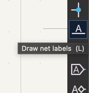
- "Draw Net Labels (L)" is used to label connections, reducing the need for wires and providing a cleaner, more organized view of the schematic. Net labels indicate connectivity across different parts of the design without cluttering the diagram with excessive wiring.
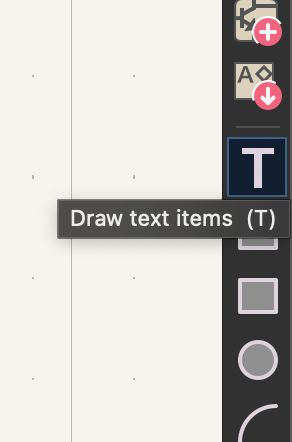
- "Draw Text (T)" allows you to add notes and annotations to the schematic. This is useful for including additional information, explanations, or comments that can help in understanding the design or providing instructions to others who may work on the project.
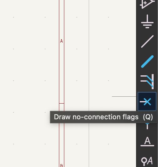
- "No Connection Flags (Q)" are used for marking pins that have no connection. This helps in identifying and clarifying that certain pins are intentionally left unconnected, avoiding confusion and potential errors during the design process.
The kid who wanted to fly high.
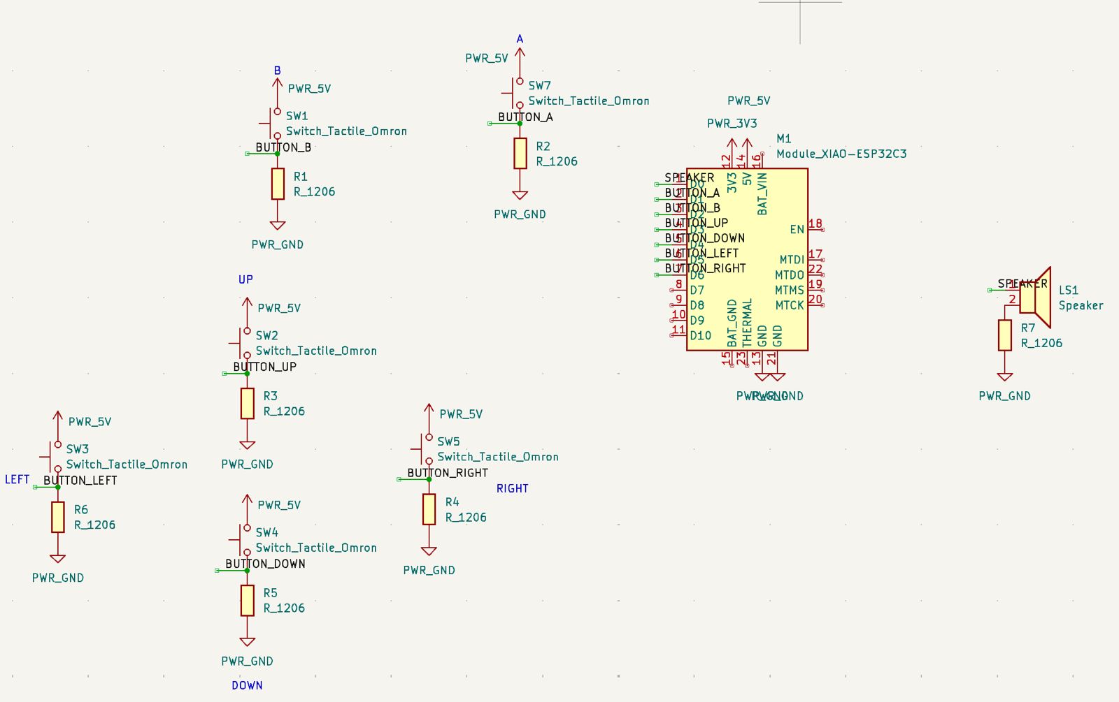
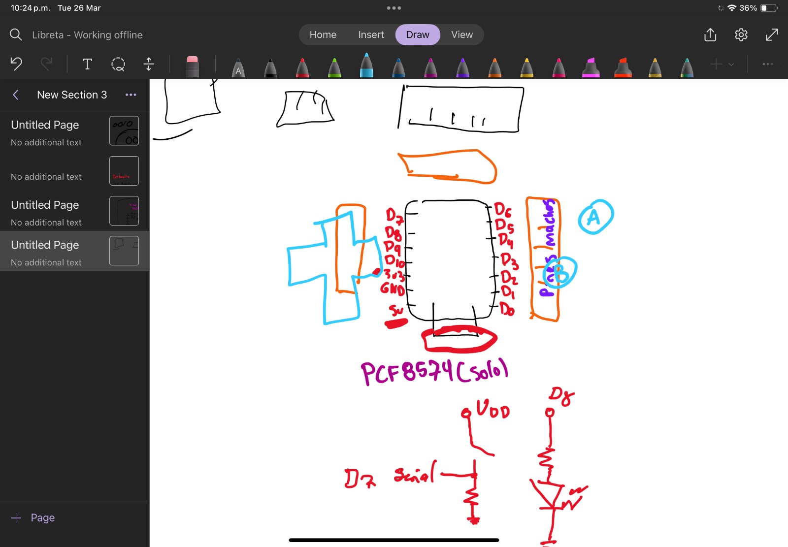
My vision was to start with the essentials: the directional pad and the quintessential A and B buttons, drawing inspiration from classic gaming consoles.
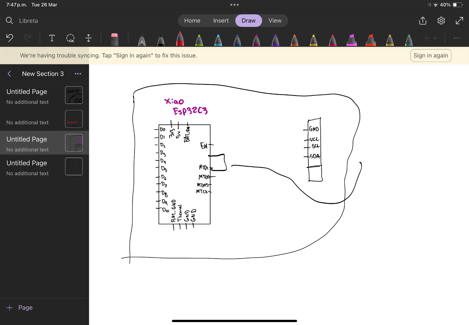
Choosing the Xiao ESP32C3 microcontroller was a strategic move for "The GameShine," driven by its compactness, wireless functionality, and numerous GPIO pins for input flexibility and future additions like speakers. The FabLab's library, which included the Xiao ESP32C3 complete with its datasheet, was instrumental in the design process, providing essential information that greatly facilitated the development of the controller.
I leveraged Flux.AI to identify the most beneficial pins for connecting peripherals to the Xiao ESP32C3. This tool helped me analyze the microcontroller's pinout, ensuring optimal utilization of its capabilities for "The GameShine" project.
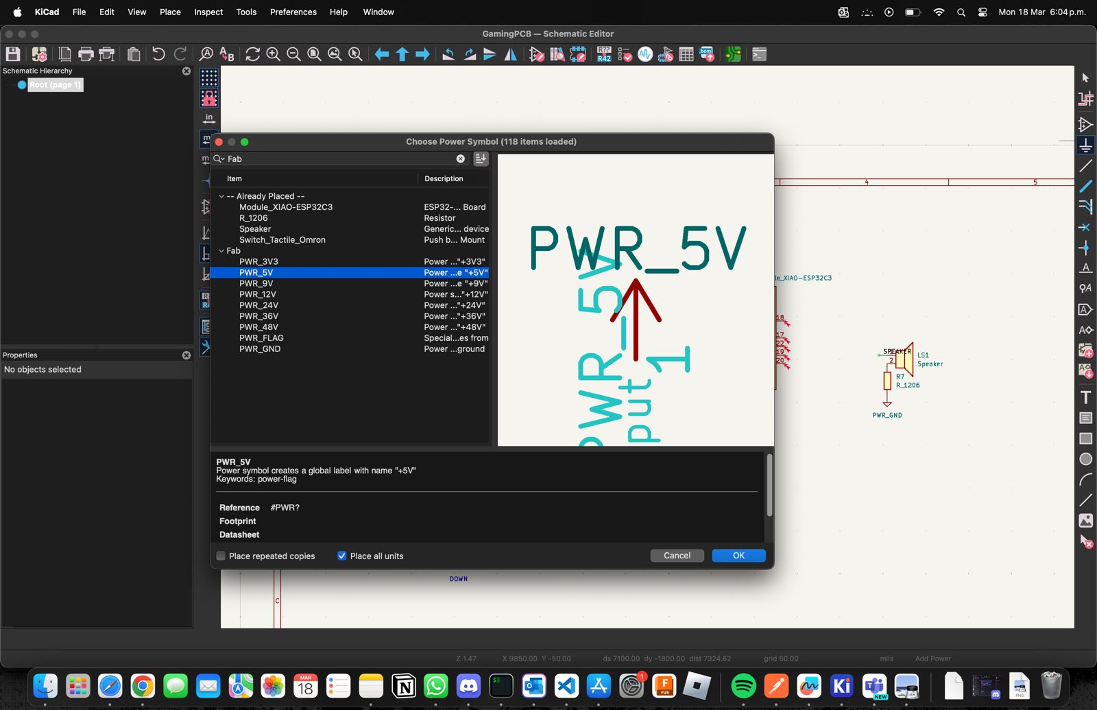
In KiCad, incorporating buttons and resistances from the FabLab library added depth to "The GameShine" project. We specifically used an R_1206 resistor and a switch tactile Omron, carefully selected for their compatibility and functionality. Additionally, we integrated power symbols for 5V and GND, crucial for defining the power supply routes within the circuit. These elements, methodically chosen and placed, contributed significantly to the foundational structure of the game controller's design.
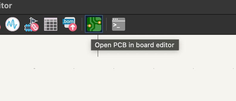
After finalizing my schematic in KiCad's Schematic Editor, I proceed to the PCB design phase by clicking on the “Open in PCB Editor” button. This action launches the PCB Editor, where I begin the physical layout of my circuit. Initially, the components are not shown but we are now on the necessary screen to do that.
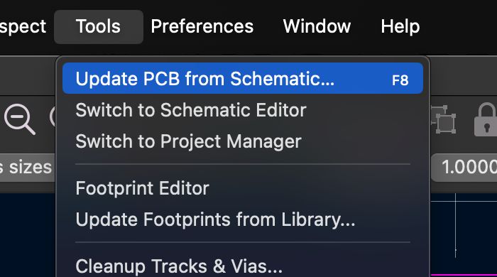
Inside the PCB Editor, my first task is to import the components and their interconnections from the schematic. This is done by selecting the “Update PCB from Schematic” button. KiCad presents a dialog showing all components and nets to be imported into the PCB layout. Upon confirming, all components from the schematic appear in the PCB Editor as unplaced footprints, usually gathered around the board's perimeter.
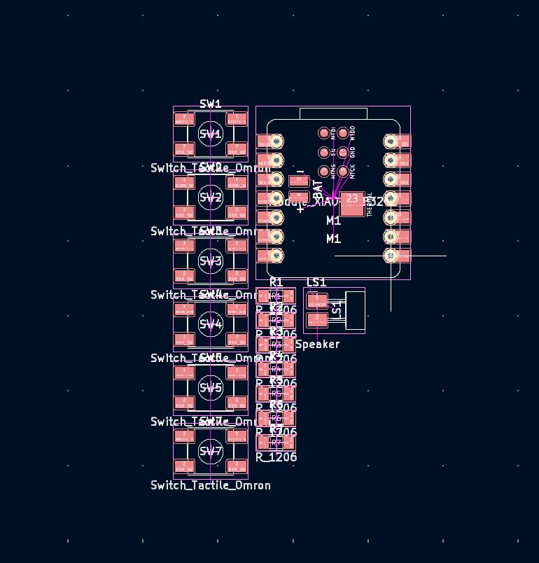
The next step involves placing these components on the PCB. Initially, I place them based on the circuit's requirements, thinking ahead about how they will connect to streamline the routing process later. This placement doesn't need to be final; adjustments are common as I proceed with routing the connections.
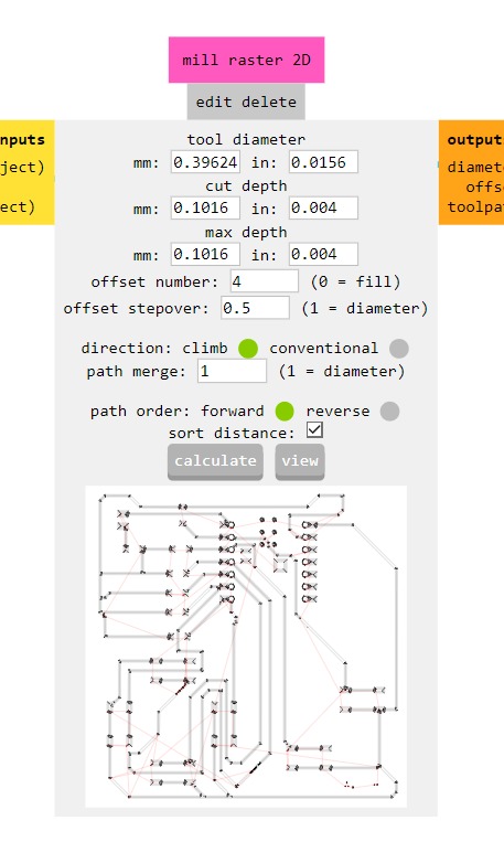
Next we will work on the F.Cu (Front Copper) layer. This layer is critical because it determines where the copper will be left on the board during the etching process, forming the electrical pathways between components. When preparing the PCB for the milling machine, the F.Cu layer's design informs the engraving process. The machine removes copper only where there are no traces, leaving behind the circuit as designed in KiCad. This precision allows for the creation of complex circuits on relatively small pieces of PCB material.
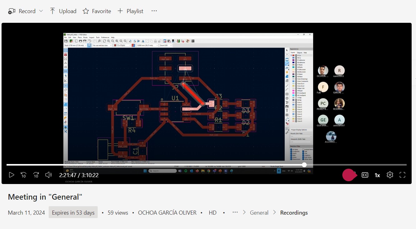
With the components placed, I begin routing using the Wire Tool. This tool enables me to draw traces, the physical connections, between components. KiCad intelligently highlights where each trace should go, based on my schematic design. The real challenge is routing all connections without overlaps or intersections, much like untangling a wire puzzle. This step often involves strategic planning and adjustment to ensure a clean, efficient layout.
Once all connections are routed, I focus on refining and optimizing the layout. This crucial step involves repositioning components and rerouting traces to minimize their length and avoid potential issues, such as electromagnetic interference. Optimization ensures the PCB is not only functional but also meets manufacturing standards. Warning: This will take you a lot of time if you aren't good at puzzles like me lol.
One of the things I lacked in this attempt was the definition of design rules. In this attempt I had only modified the pre-defined sizes to 0.6mm which had caused a lot of problems with the mods page. To see the proper design rules please check the May 6 Update!
Finalizing the flight...
In the process of finalizing a PCB design in KiCad, adding specific layers plays a crucial role in defining the physical characteristics of the board and facilitating its manufacturing.
The first layer I work with is the Edge Cuts layer. This layer is essential for defining the physical boundary of the PCB. By drawing on this layer, I specify the exact shape and dimensions of the board's edges. This step is crucial not only for the aesthetic aspect of the PCB but also for ensuring it fits within any designated enclosure or aligns with other hardware components. When the PCB is manufactured, the milling machine uses the edge cuts as a guide to trim the board to its final shape. Precision in this step is key, as any discrepancy can lead to fitting issues down the line.
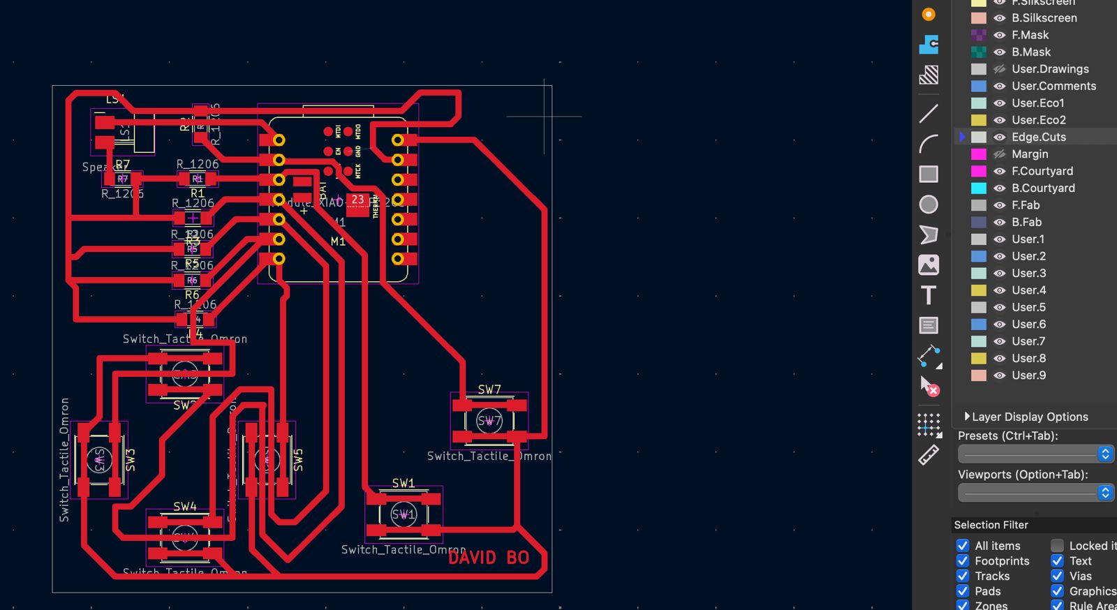
Next, I add a Margin layer. This layer provides an additional boundary outside the edge cuts. The purpose of the margin is multifaceted. Primarily, it acts as a safety buffer during the PCB manufacturing process, ensuring that no critical components or traces are too close to the edge of the board.
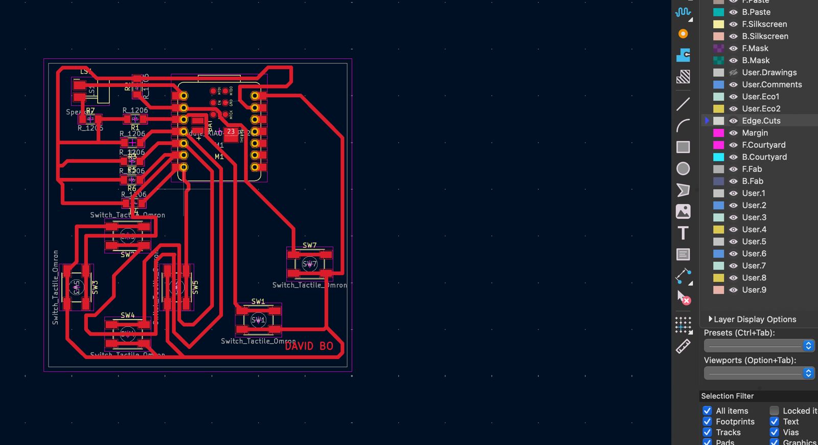
The User.Drawings layer serves a unique purpose in my design process. I use this layer to mark areas of the PCB that need to be hidden or protected during certain manufacturing processes, such as milling. For example, if there are sections of the board that should not be exposed to the milling machine for any reason, I can denote these on the User.Drawings layer. This technique is particularly useful when preparing the PCB for manufacturing, as it allows for greater control over the outcome of the milling and cutting processes.
I proceeded to the crucial step of exporting my design. The aim was to prepare it for the actual manufacturing phase, specifically for use with a PCB milling machine. For this purpose, I selected two layers to export: the F.Cu (Front Copper) and the User.Drawings layers.
And now... the crash :(
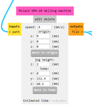
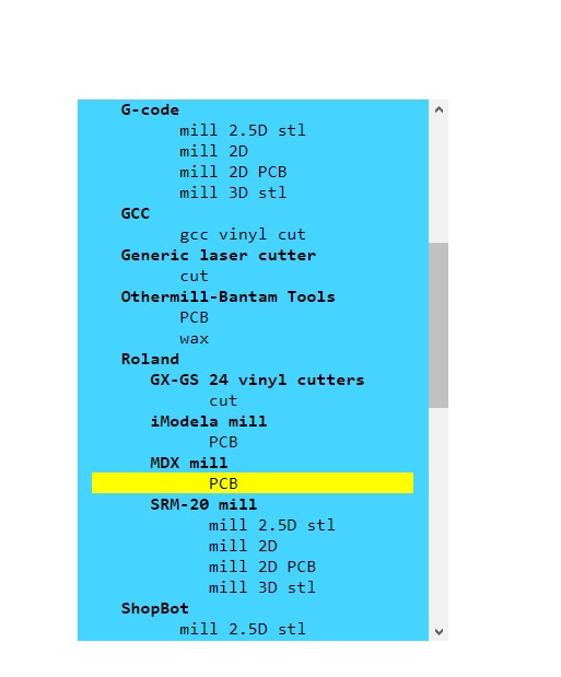
The Roland SRM-20...
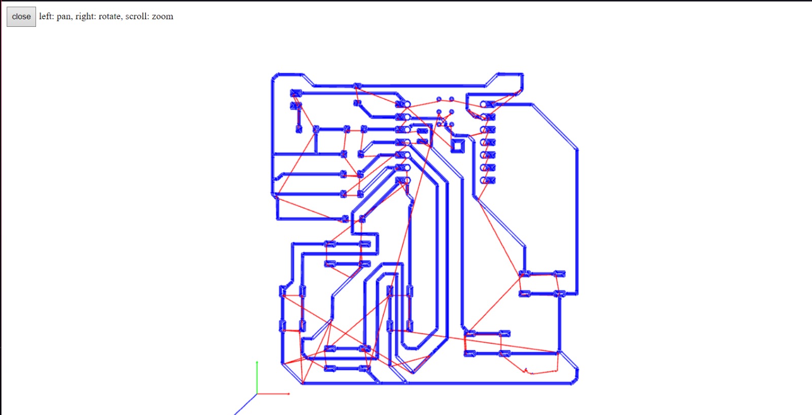
Using the ROLAND SRM-20 for milling PCBs was an intricate process, which involved both preparing the design files and understanding the machine's operation. My experience began with creating the design for the PCB, for which I used the modsproject.org website. This platform was instrumental in converting my PCB design into a format suitable for the milling machine. The website's user-friendly interface allowed me to input my design and tweak various parameters, ensuring that the output file would be precisely aligned with the capabilities of the ROLAND SRM-20.
For this we used the modsproject.org website that we had previously seen on Week 04.
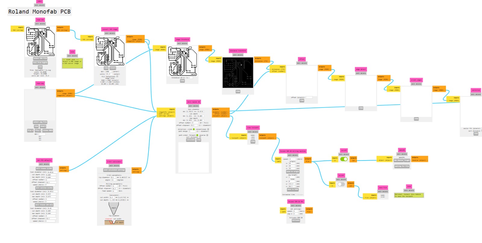
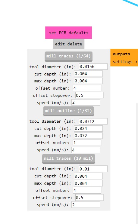
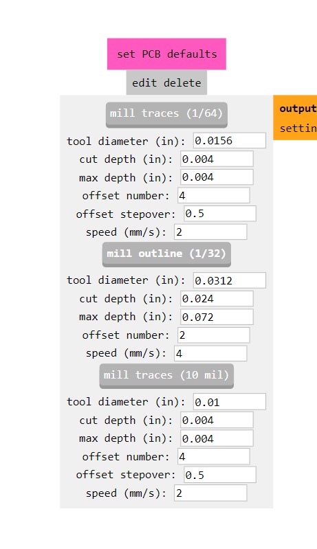
From here we needed to modify some settings that I didn't place on Week04.
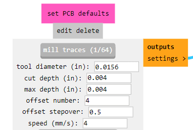
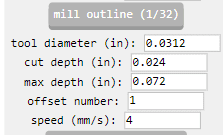
For the traces:
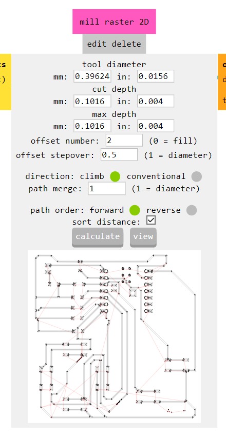
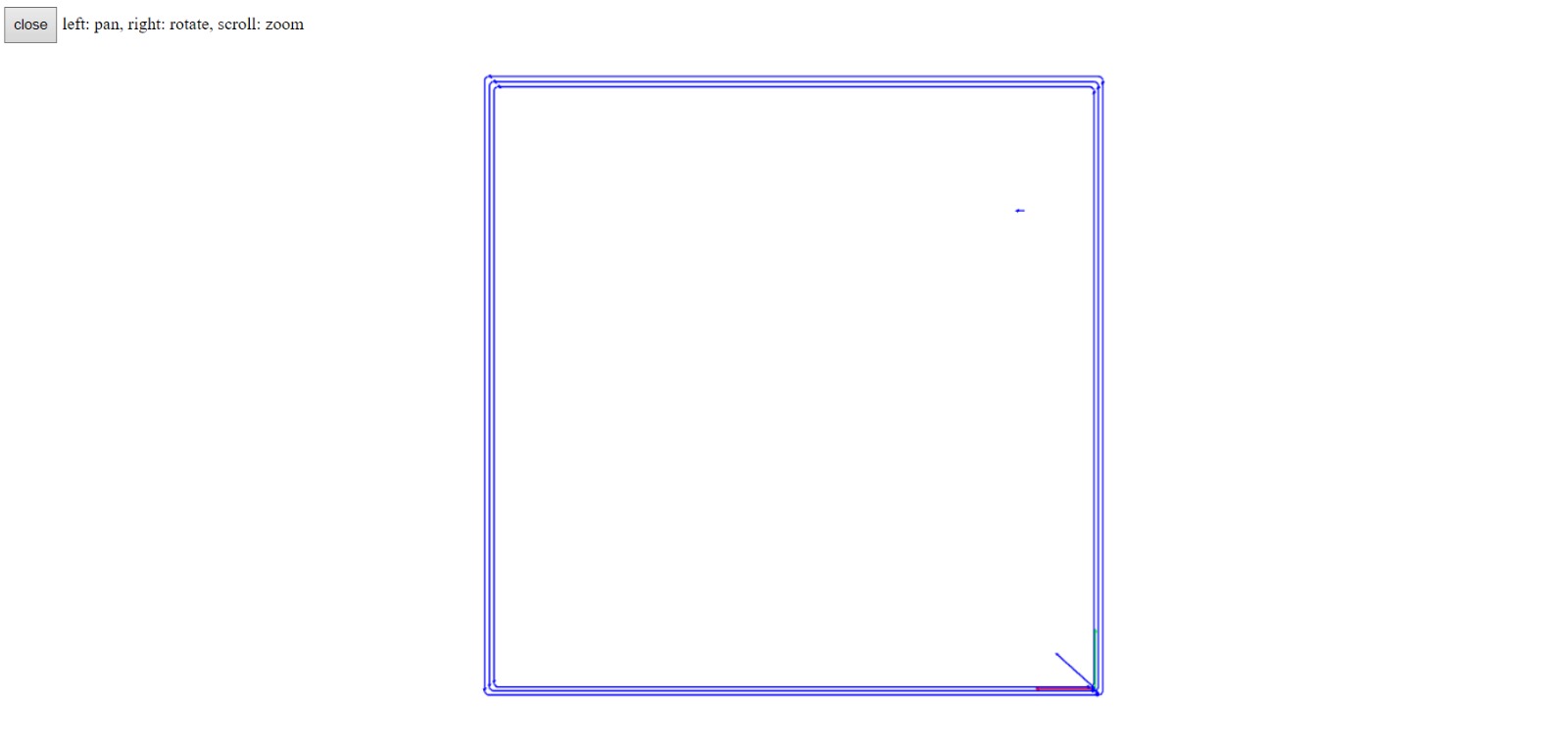
If done correctly, a pop-up windowh should appear with the engraving trajectory:
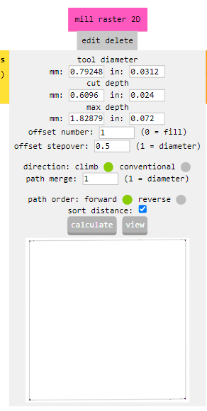
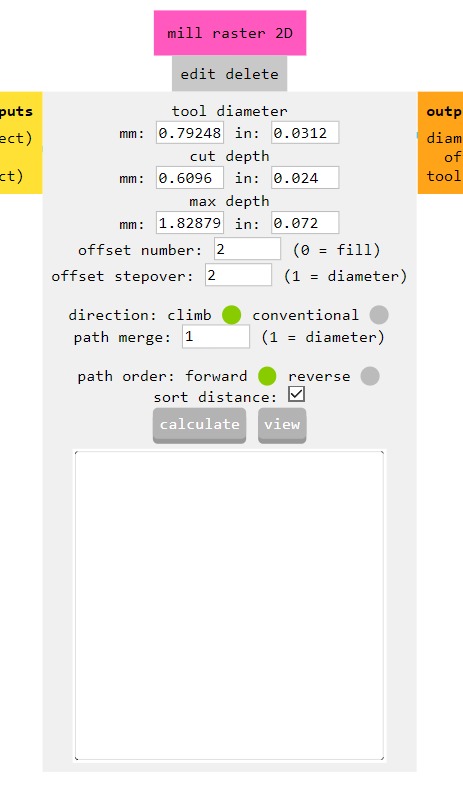
For the cut:
From here, we can send it to VPanel for SRM-20. However I still had the complication from before and that was that my Mac isn't capable of running that program even with a Virtual Machine so I had to wait until someone lend me their computer since the instructors weren't present that day.
The VPanel software:
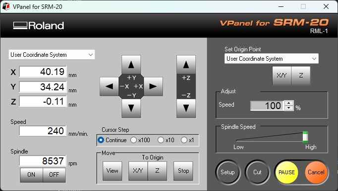
Once we had calibrated the Z axis and inserted our tool. It was time to cut. So I loaded the .rml file that the modsproject gave me.
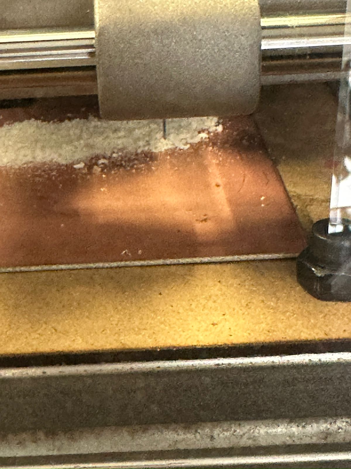
And then, disaster struck...
The tool broke in front of my eyes and, even when I had scheduled my appointment with the SRM-20 with an instructor, there wasn't any instructor present that day that could help me since everybody left extremely early.
Not only that, but due to this error the other 6 people that were also scheduled that day had to be delayed because there wasn't any way we could cut.
Want to see how the PCB turned out with this mistake? Well, here is a trigger warning since it will look really really ugly...
After reviewing my file I have seen that I hadn't turned on correctly the the mill traces (1/64) and that is why it began to cut and pierce through the copper board. A rookie mistake of my part.
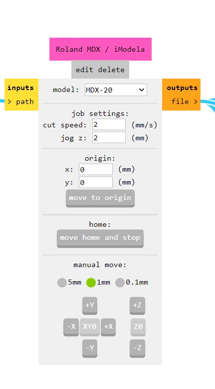
The Modela...
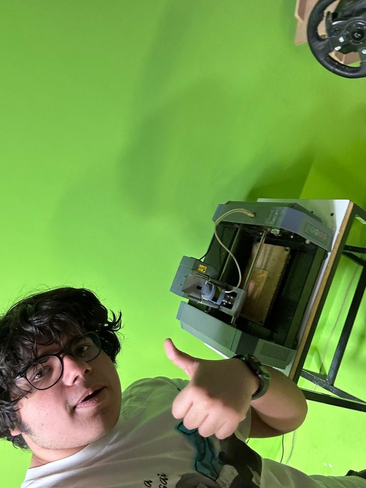
Not wanting to give up, I ran urgently the next day to get a new milling CNC that could help me get the PCB done quickly. This is where I found an old modela in the FabLab, this old modela you may have seen on previous years working but now, well... it was really really outdated.
The Roland Modela MDX-20 is a versatile desktop milling and 3D scanning device, supporting a broad range of 3D CAD applications. It's capable of milling materials including ABS, acrylic, wood, plaster, styrene foam, chemical wood, wax, and softer metals like aluminum and brass. Compatible with Modela software, it accepts file types such as .STL, .DXF, and .MDJ.
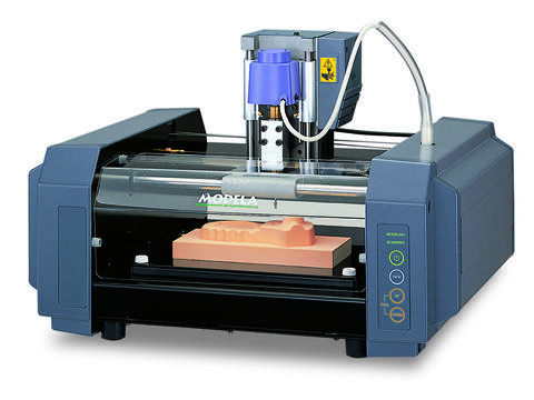
Specifications:
- Maximum Working Area: 203.2 mm (X) x 152.4 mm (Y) x 60.5 mm (Z)
- Maximum Table Load Weight: 1 kg (2.2 Ibs)
- Compatible Materials: ABS, acrylic, wood, plaster, styrene foam, chemical wood, wax, plaster, polyacetal, polycarbonate, Sandomur SS, aluminum, brass
- Weight of Unit: 13.7 kg (30.2 Ibs)
Just like with the SRM-20 we needed to get our .RML files but now for the Modela. For this please follow the following steps:
The traces:
If done correctly, you should get a pop-up screen like this one:
The cut:
If done correctly a pop-up screen should appear like this one:
Now all that was left was to send it to the Modela... R-Right?
My experience with the Roland Modela MDX-20 was far from smooth, highlighting the challenges of working with outdated technology. Despite its reputation as a versatile desktop milling and 3D scanning device, the MDX-20 showed its age, most notably through a malfunctioning z-axis. This critical issue significantly hampered its functionality, making it difficult to rely on for precise tasks such as PCB milling. As the deadlines for my project loomed closer, the unreliability of this equipment became a growing concern, particularly as other students encountered similar issues, leading to delays and further strain on the available resources.
In the midst of these challenges, my professor, Rafael Aguirre, stepped in to provide invaluable assistance. His expertise and familiarity with the MDX-20 were crucial in navigating its quirks and limitations, allowing me to proceed with milling my PCB despite the ongoing issues. His intervention underscored the importance of experienced guidance when dealing with specialized, albeit outdated, equipment. Without his help, meeting my project deadlines would have been significantly more difficult, if not impossible, given the continuous breakdowns and the high demand on the more reliable SRM-20 machine from other students.
The software interface of the Modela MDX-20 further compounded the difficulties. Contrary to claims of user-friendliness touted on its website, the software was anything but intuitive. Its design felt archaic, with a user interface that could only be described as unattractive and cumbersome to navigate. This steep learning curve and lack of intuitive design made the milling process more time-consuming and frustrating than necessary. Every step required careful attention, and the lack of modern usability features starkly highlighted how far behind current standards the software had fallen.
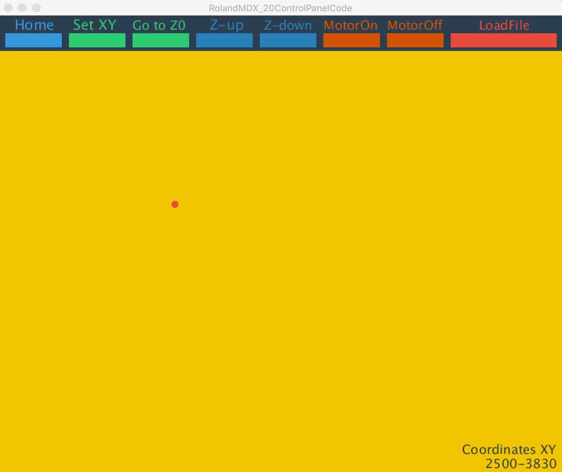
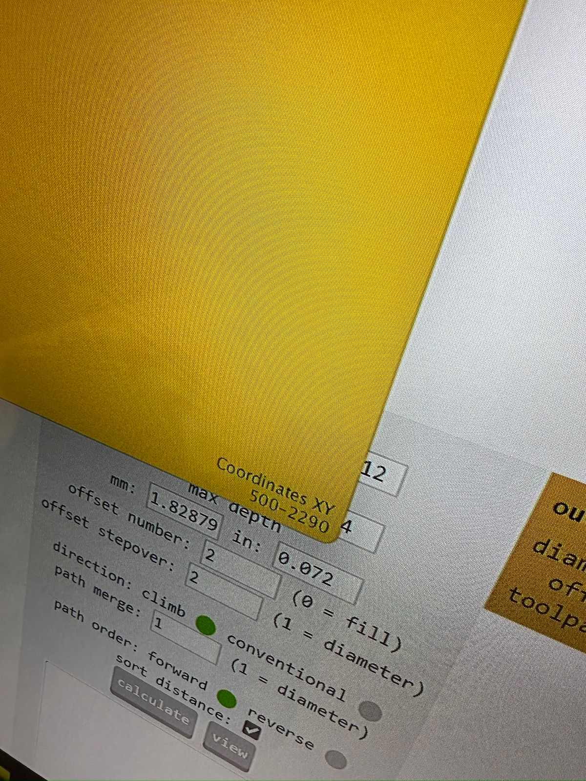
Operating the MDX-20 involved a peculiar and rather finicky method of setting the X and Y coordinates using a matrix. This approach, far from being straightforward, introduced an additional layer of complexity to the milling process. To make matters worse, the machine's reliability was questionable at best, with frequent breakdowns occurring roughly every 10 minutes of operation. This instability not only disrupted the workflow but also heightened the anxiety of racing against time to complete my PCB. Navigating these technical hurdles with such outdated equipment tested my patience and resilience, underscoring the pressing need for accessible, reliable, and user-friendly technology in educational settings.
An example of how the coordinates where shown in the software and how I needed to do that everytime the Modela disconnected...
With this in mind, here is an step-by-step process of how to setup the Modela.
- Start the machine with the power button.
- Place the engraving tip and adjust it.
- Press the view button to locate the tip in the coordinate you see fit (in my case, 500-2290).
- Lower the tip on the Z axis with the UP and DOWN buttons in order to locate it better.
- Open the RolandMDX_20ControlPanelCode software
- Position the tip as close as possible to the PCB, initiating the engraving process. Using a sheet of paper placed beneath the tip, gradually lower it until it just begins to tear through the paper, indicating the correct depth has been reached.
- In the software we establish the coordinates of origin X and Y
- Load .RML file.
- Program will begin to engrave the design.
Despite all of these challenges, I went for it. I got my copper sheet off my sacrifice bed and pasted it with double-sided tape into the sacrifice bed of the Modela. And then, loaded the file.
All that was left to do was to pray. Technically I hadn't done anything wrong and it all depended on the Modela doing it's work correctly and that time didn't mess up it's precision.
And when it was about to be done... THE TIP BROKE.
Even though I quickly stopped the machine, it was too late. I had to find a new tip to quickly replace it and make sure that hte tip was in the exact position it was at. However, the Modela played me dirty and it also changed the coordinates of the axis and now it was impossible to continue doing it without doing it again.
And sadly, by that time the university had already closed and all students were required to leave.
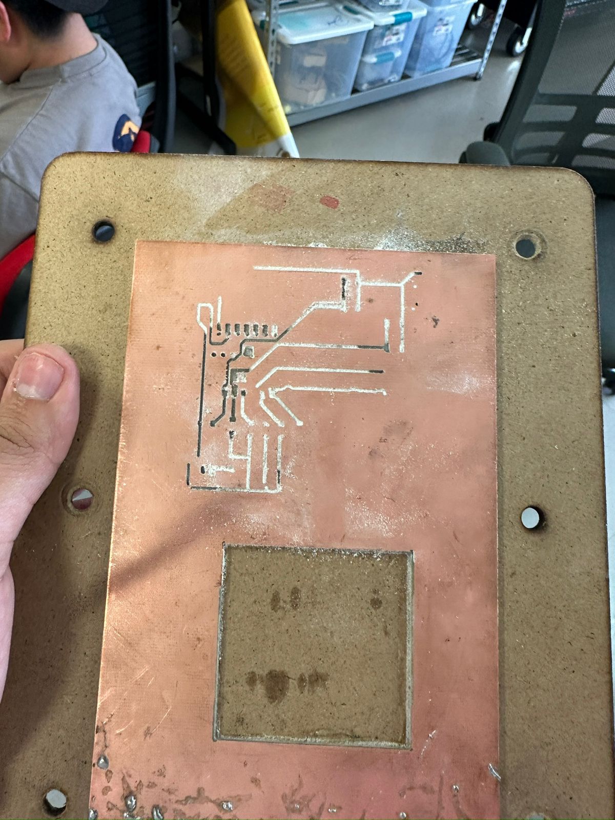
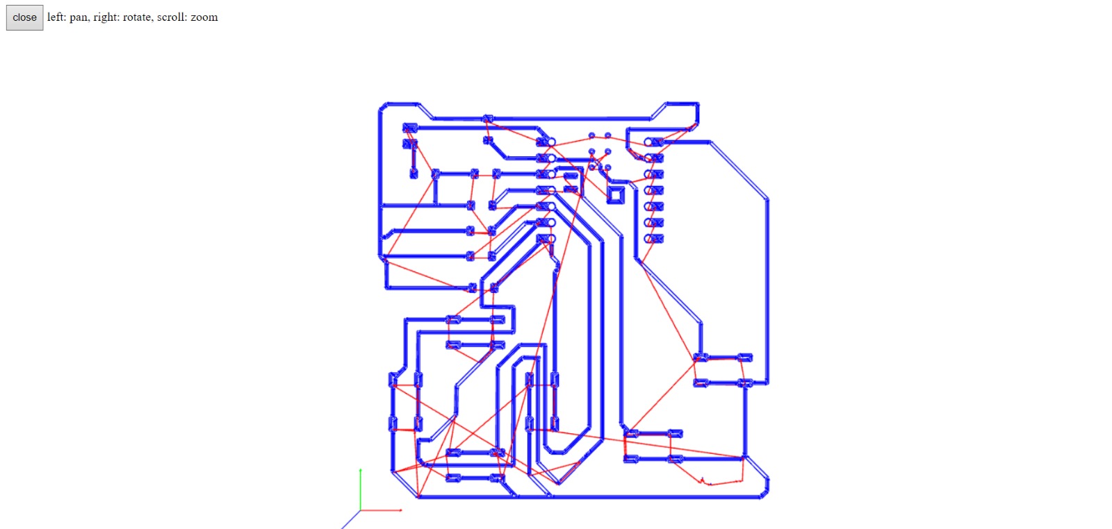
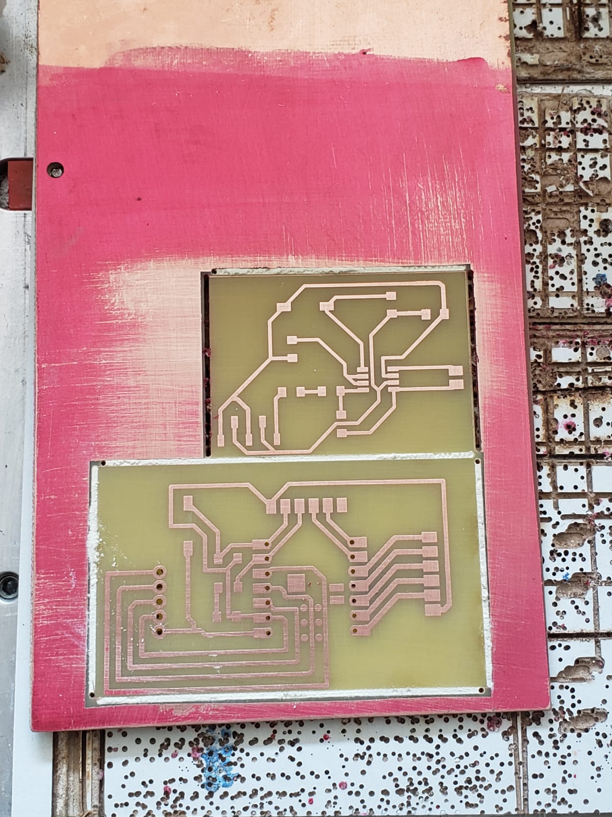
Here is what my board looked like. As you can see only the corners, left button and some connections with the resistances were missing. It was almost done and the 4 days I had spent working on trying to mill with the Modela were now gone to waste.
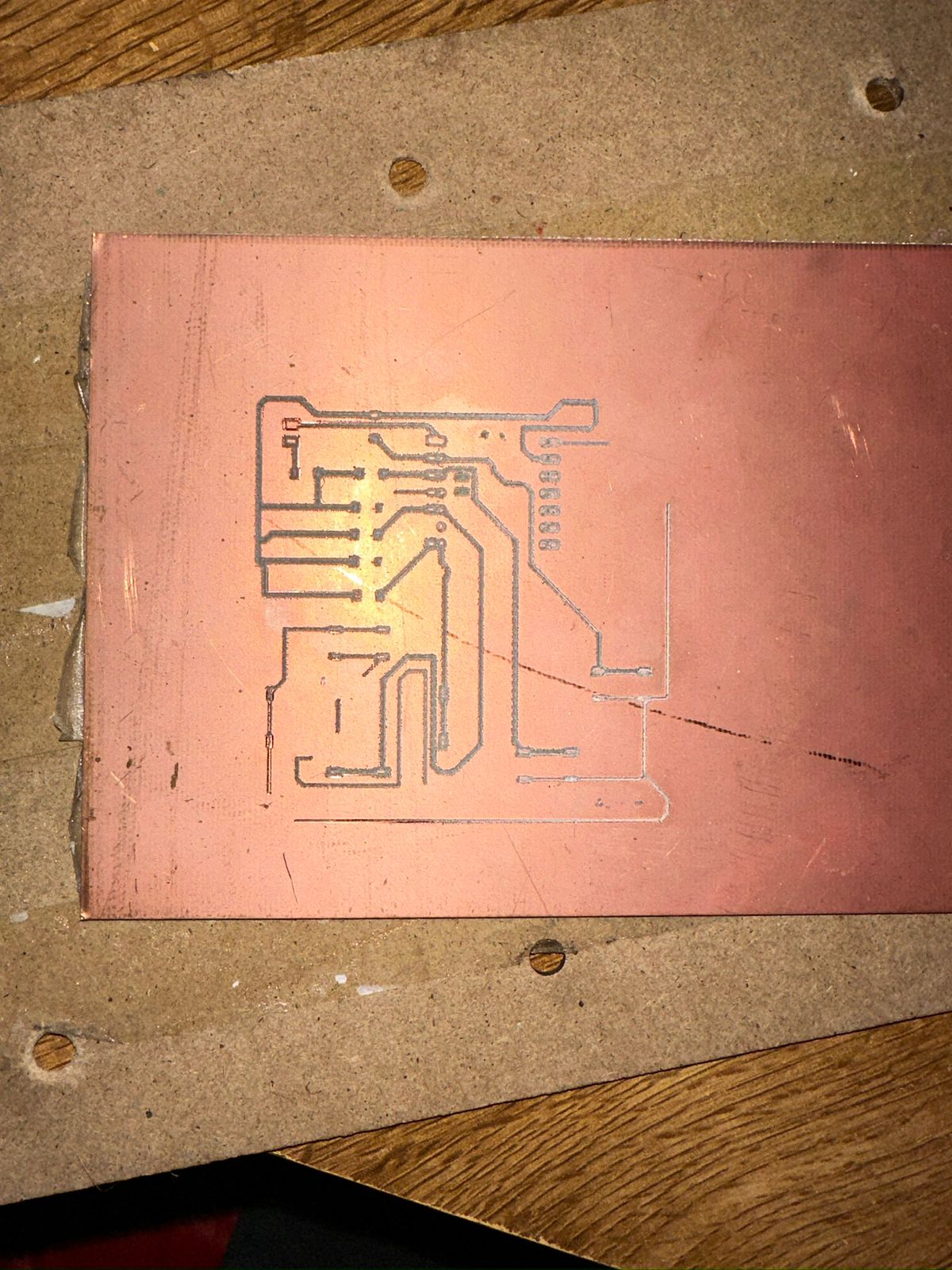
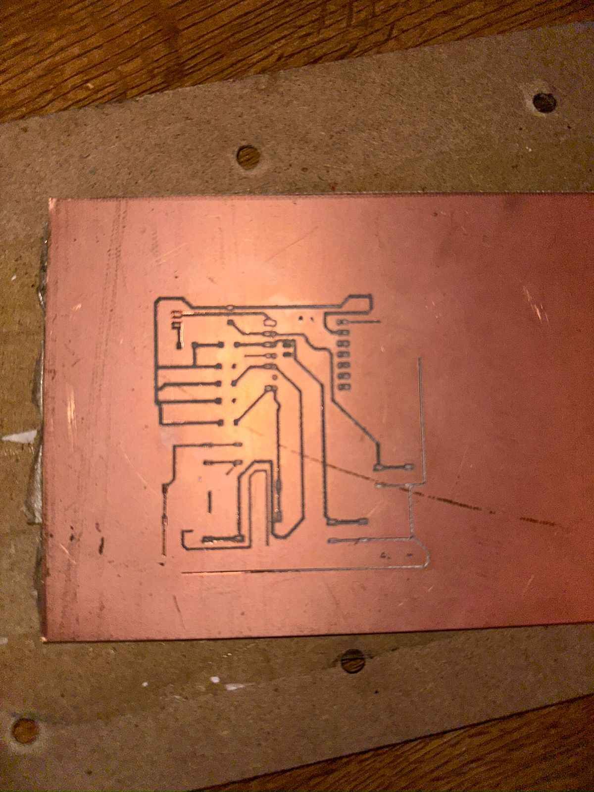
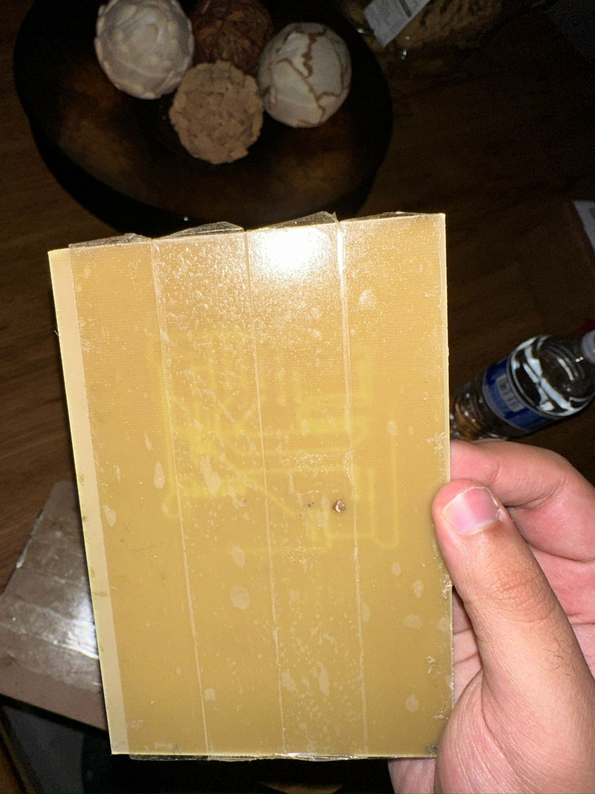
Also, it appears that the tool ate the incorrect parts of the copper so even if I wanted to connect something it would cause a short circuit and possibly damage my components. That is why I didn't take the risk to solder anything without a proper PCB milled out. Update of last minute: Now I know why it did that, it appears I needed to invert the image for it to cut correctly :(
In addition, there was a huge mistake in how I generated the white and black png files for the traces. I needed to have the trackes in black over the board in white. Because of this I had a huge major issue with the attempts at milling the PCBs because I always cutted away the copper of the traces instead of cutting away the copper around the traces.
And so, this week failed! Yay :(
Conclusion:
Reflecting on this week's challenges and setbacks, I find myself confronting a mix of emotions, predominantly feelings of disappointment and a sense of hopelessness. My ambition, though fueled by a genuine passion for completing my final project, might have led me astray, causing me to bypass the meticulous and gradual approach essential in electronics design. This oversight resulted in a series of avoidable errors, further compounded by the difficulty in finding collaborative support within the bustling environment of the Fab Lab. The realization that I had ventured too far too fast, without the necessary guidance or assistance, was a bitter pill to swallow.
Amidst this turmoil, I had already taken steps based on the optimistic assumption of smooth progress. I ordered a Xiao, anticipating that it would arrive just in time to integrate into my freshly milled PCB. This anticipation added a layer of pressure, as the ticking clock seemed to mock my unanticipated delays. The situation felt increasingly dire, casting a shadow over my initial excitement and replacing it with a looming sense of defeat.
Compounding this, I had also invested in a complete soldering kit, planning to dedicate my nights to assembling the project as soon as the milling was done. This proactive approach, meant to save time, now felt like a mocking reminder of my overly ambitious planning. The tools and components sat idle, waiting for a project that was still far from ready, highlighting the gap between my expectations and the reality of my progress.
In conclusion, this week has been a humbling experience, underscoring the crucial lesson that ambition must be tempered with patience and realism. The feelings of hopelessness and frustration that ensued from my eagerness to progress too quickly have taught me the importance of adopting a more measured and thoughtful approach to project work. Success, as I've painfully learned, is not solely about pushing forward with individual effort but also about recognizing when to seek out and accept help. As I look towards the future, I am reminded that in the pursuit of achievement, sometimes the bravest step is to pause, reassess, and proceed with caution and collaboration.
Bonus: A fire!
While writing this I began to smell burnt wood in my home. Then I got a message from my mother that told me there was a fire going on, I went expecting a small fire like one in the kitchen or something but...

The house in front of mine was burning and I have never seen a flame so big in my life. I stayed up until 1am helping the firefighters with water buckets from my home! I know this isn't relevant but I just wanted to share this and yeah, this wasn't my week at all lol.
Update May 6: Game Over - Would you like to continue?
FabAcademy: Episode IV - A new hope
After all the suffering I finally got back up and designed a new board.
The design process started with detailed sketches to envision the modular layout, which was crucial for integrating both electronic principles and ergonomic considerations. These preliminary drawings served as a comprehensive blueprint, guiding the systematic placement of components and ensuring a balance between technical requirements and user interface.
Central to the redesign was the strategic placement of the Xiao module. I positioned the USB-C connector at the bottom of the PCB, mirroring the iconic Gameboy design for both aesthetic appeal and functional access for programming and power connections. Above this, I planned for additional buttons directly over the microcontroller, promoting a compact and user-friendly design.
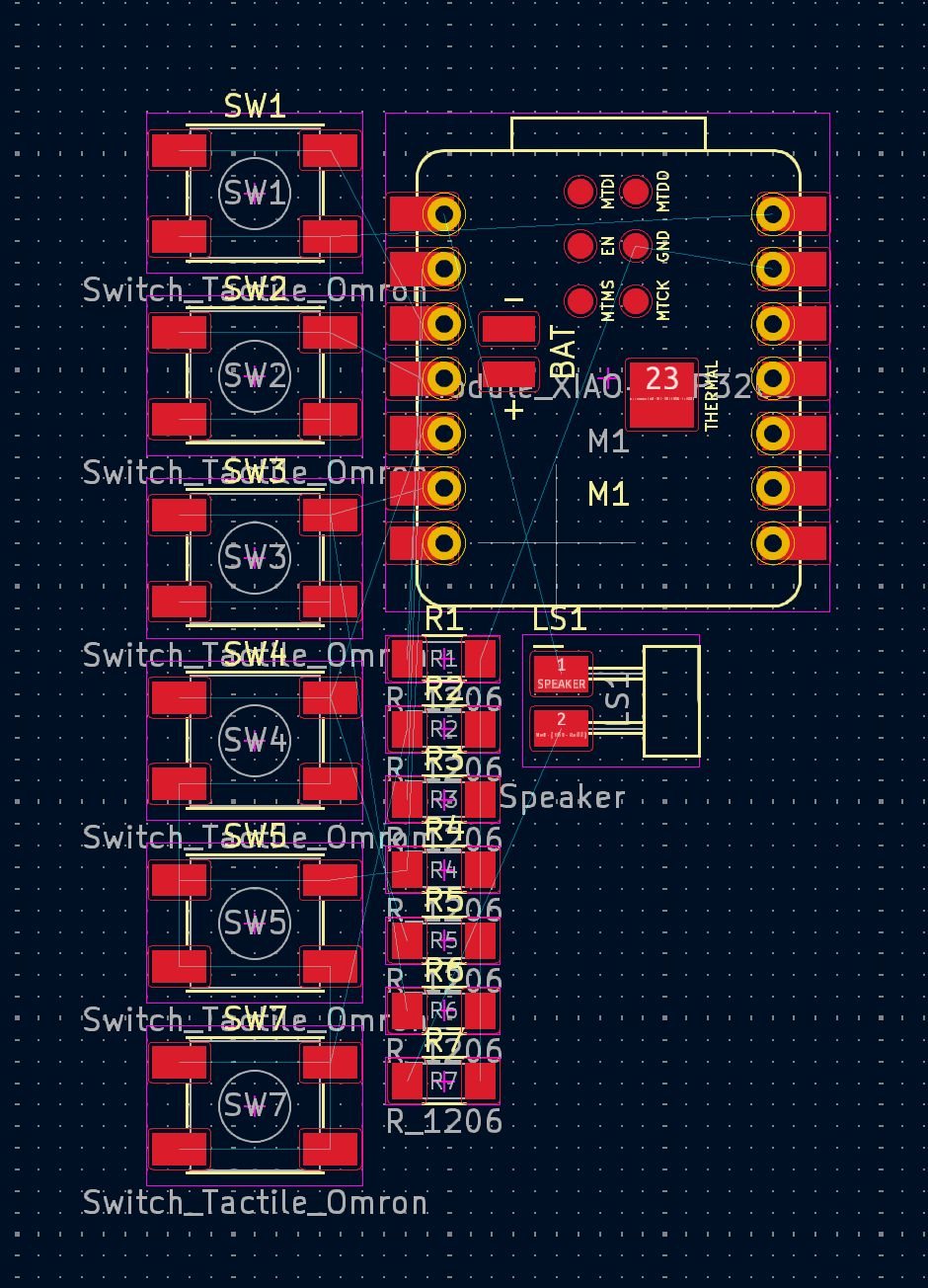
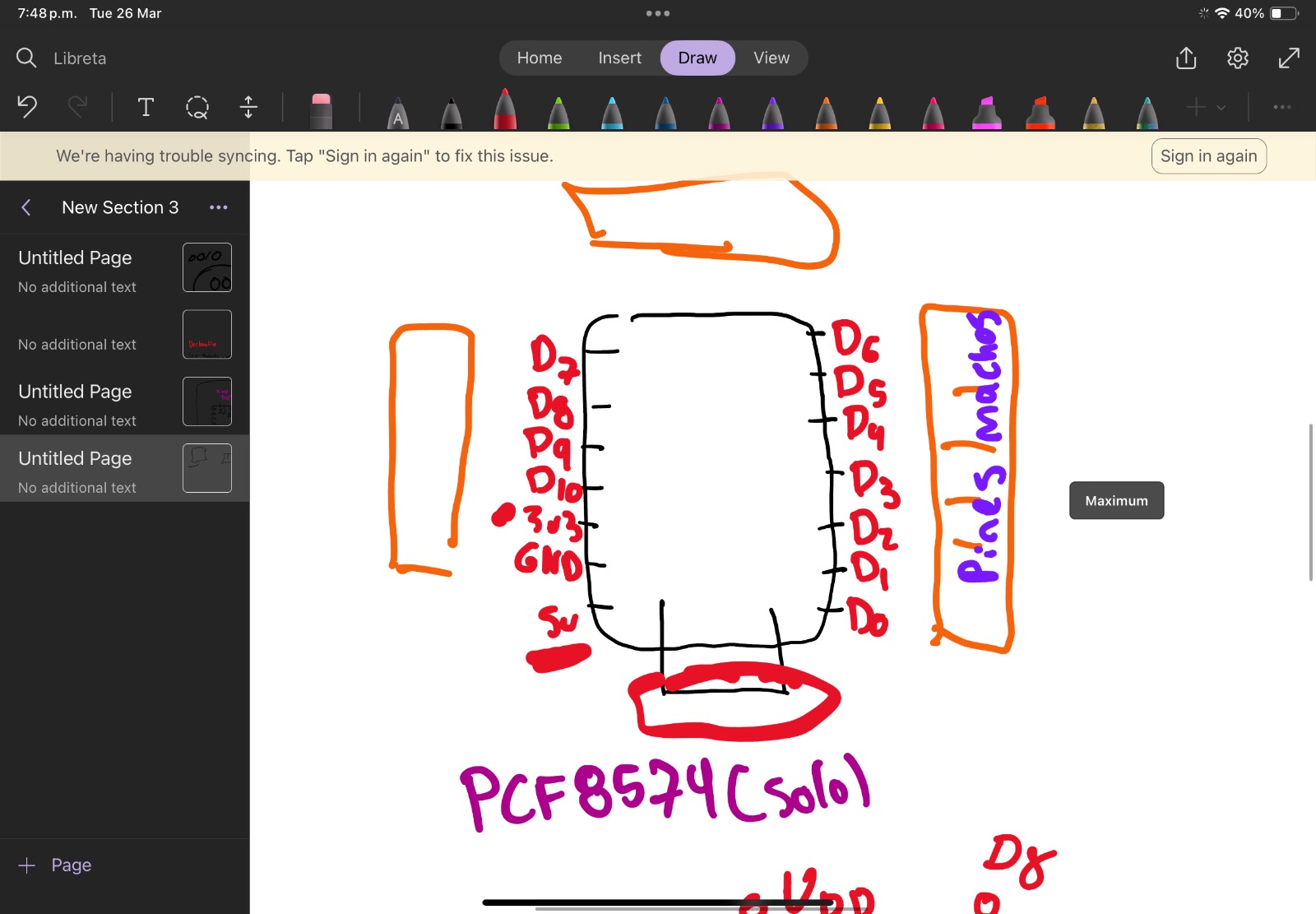
I utilized KiCad for the PCB design, retaining the component selection from my earlier attempts but pivoting to emphasize modularity. This approach afforded flexibility and adaptability in the design process. I began by mapping out the main components and connectors in the schematic, focusing on the Xiao ESP32-C3 as the core. This microcontroller, chosen for its compact size and comprehensive capabilities, was equipped with various communication interfaces and power configurations, making it ideal for my needs.
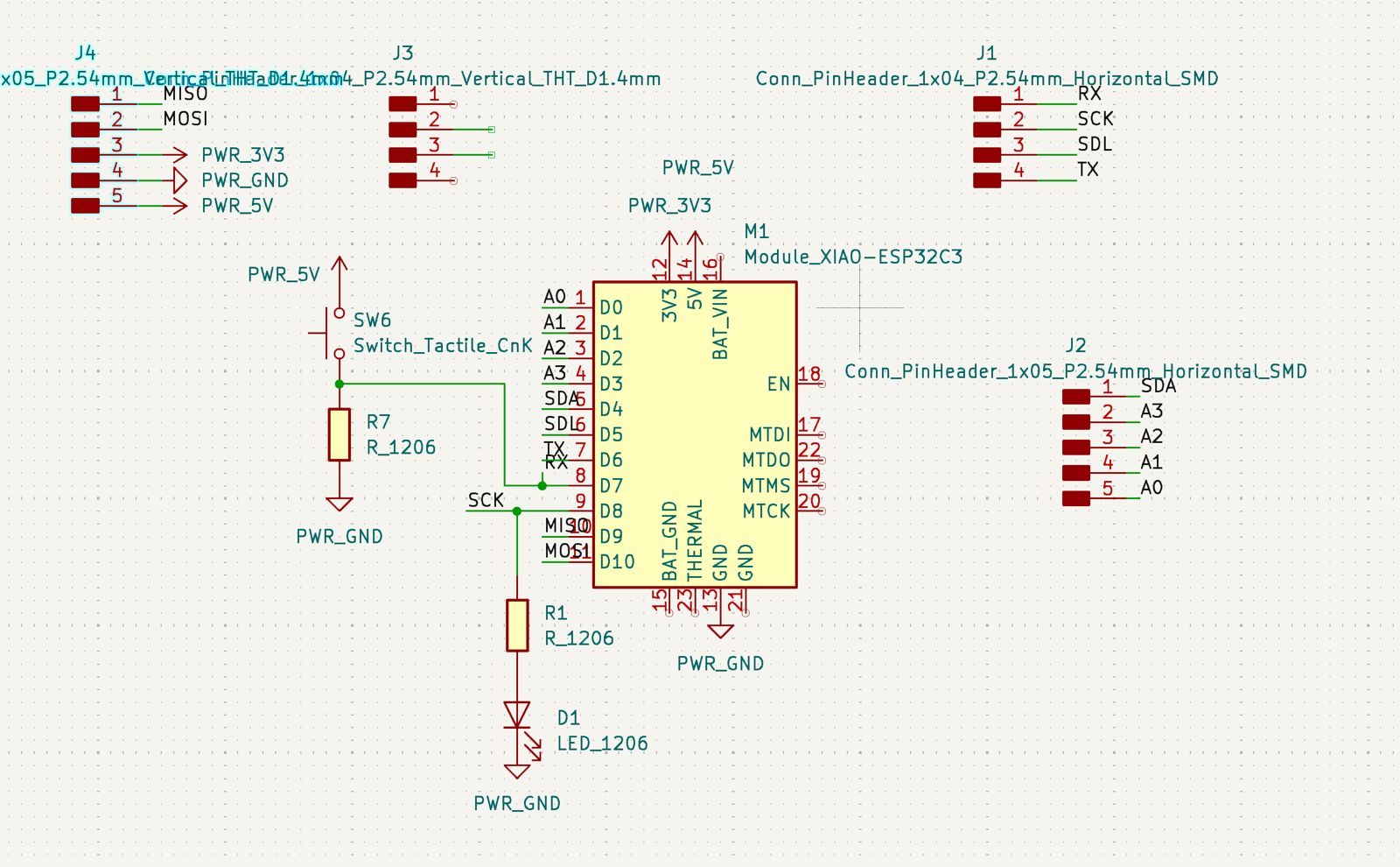
I carefully placed connectors for serial, I2C, and SPI communications along with power connections, using distinct connectors for each function to facilitate easy assembly and testing. The inclusion of basic components like resistors and a tactile switch was methodically planned to ensure stable operation and user interaction.
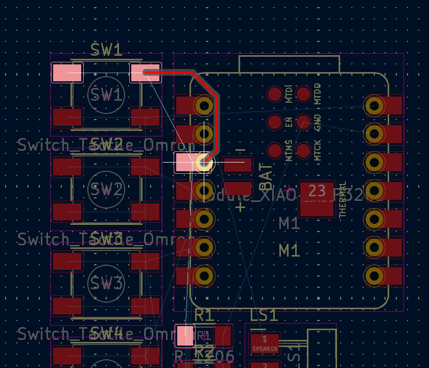
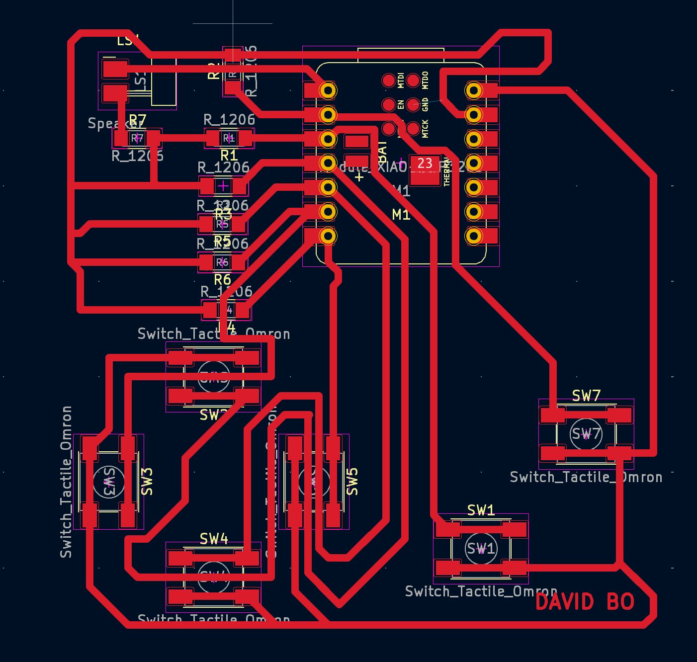
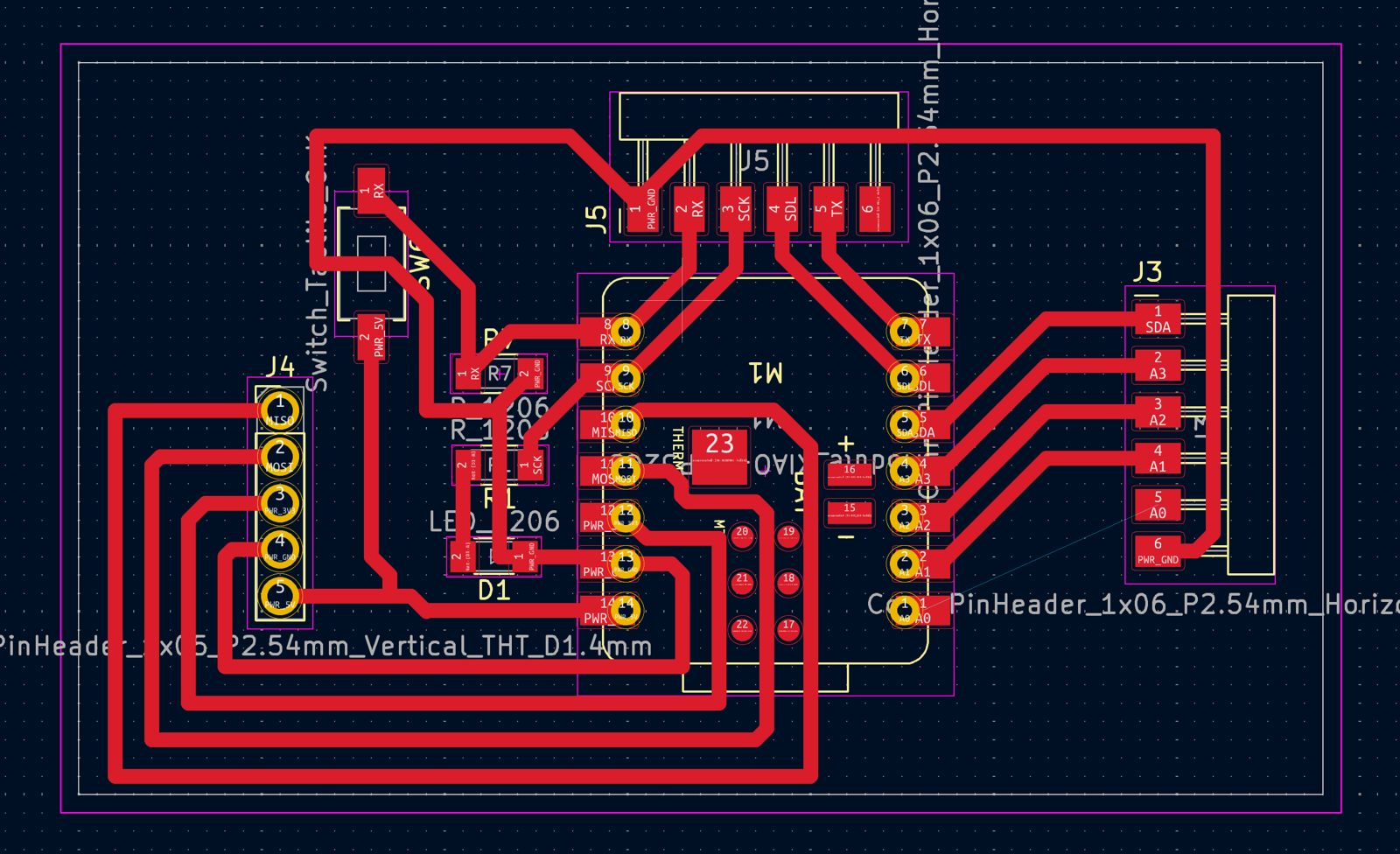
The PCB layout phase was like solving a complex puzzle, carefully arranging each component and meticulously routing connections to avoid any potential overlaps or interference, reminiscent of wire puzzle games. The challenge was to maintain clear pathways for all connections, ensuring the design was not only functional but also aesthetically pleasing.
But, before moving the rest of the components and routing them, it's essential to define stronger and more specific RULES for the paths and the design (unlike my previous attempt). This ensures that the PCB meets the necessary electrical and manufacturing standards.
- Accessing Board Setup:
- Go to 'File -> Board Setup'
- Setting Constraints:
- In the Board Setup dialog, go to the Design Rules section. Here, you can define various constraints and parameters for your PCB design.
- Modifying Clearance and Track Width:
- Set the Minimum clearance to 0.4mm. This parameter defines the smallest allowable distance between copper features on the board, such as between traces, pads, and vias. Ensuring adequate clearance is vital to prevent electrical shorts and to meet the manufacturing capabilities of your PCB fabricator.
- Set the Minimum track width to 0.5mm. This defines the narrowest width of the copper traces that can carry current on the PCB. Choosing a wider track width helps handle more current and reduces the risk of overheating, especially for power traces.
These parameters ensure that even though the components I am using do not require a lot of amperage, the chosen values play it safe by accommodating a higher current flow if needed.
-
- Pre-defined Sizes:
- In the Pre-defined Sizes section, add a track width of 0.7mm. Pre-defined sizes are useful for quickly setting trace widths during routing. This size can be used for traces that need to carry more current or for power and ground traces.
This way, when we connected every component from the PCB, it appears more organized and there are more spaces for the milling.
After completing the layout, I generated the necessary files for manufacturing, including edge cuts and user drawings, ensuring the PCB was ready for production. Despite the simpler design, careful planning and execution were crucial to avoid the issues encountered previously.
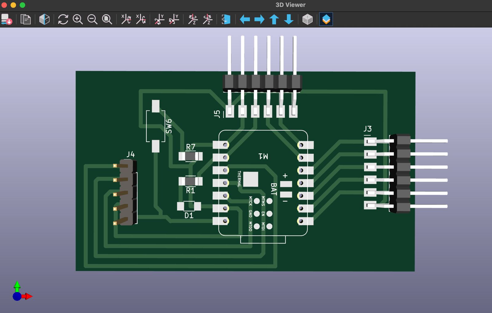
Here is a 3D visualization of the final PCB layout, reflecting the thoughtful integration of all components in a cohesive and functional design:
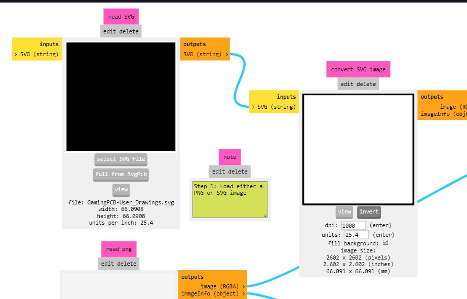
However, what I changed here was that I gave up on milling and decided to follow Neil's advice. I opted for UV printing for my PCB, which necessitated preparing specific files in KiCad.
First, I generated the Gerber files, which are the standard for PCB fabrication, detailing every aspect of the board layout from copper layers to silkscreen. Additionally, I prepared the Drill Files, essential for defining where holes should be drilled in the PCB for component leads and vias.
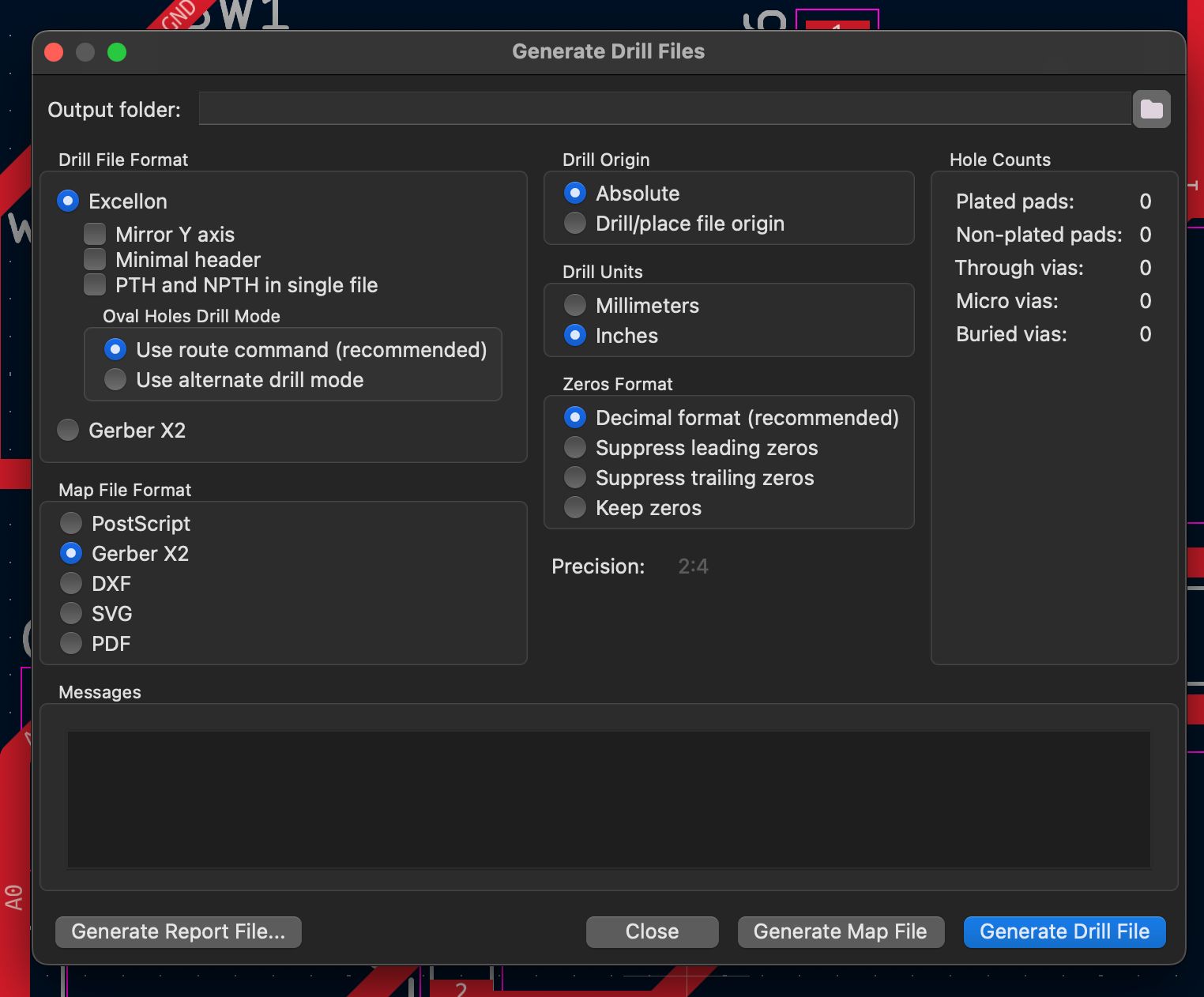
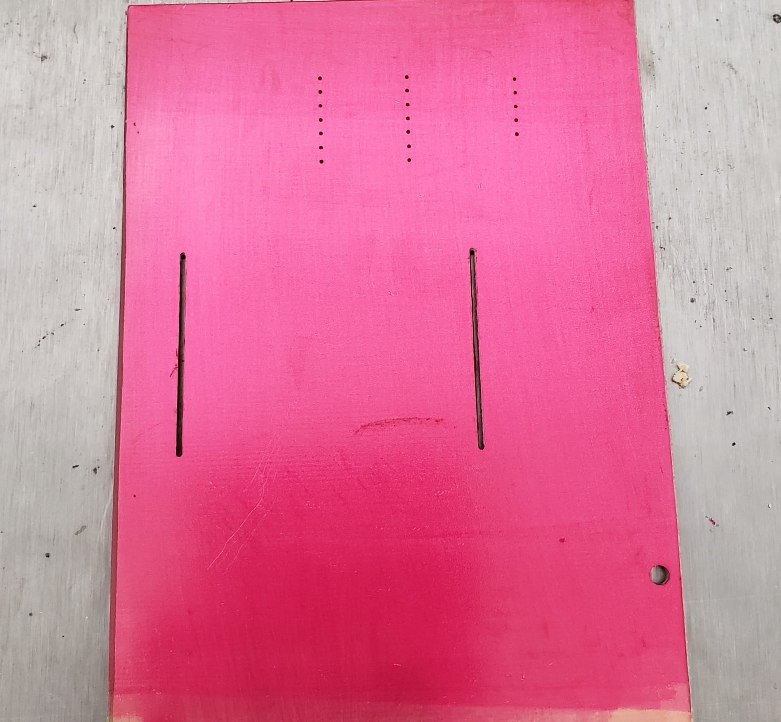
The UV printing process for my PCB began with making guide perforations or side cuts on the board as references, a crucial step especially for designs like "gammingpcb" which don't inherently require holes.
After this, a photosensitive mask was applied to the board, which was then cured in a convection oven at 80°C for 20 minutes to ensure it dried thoroughly.
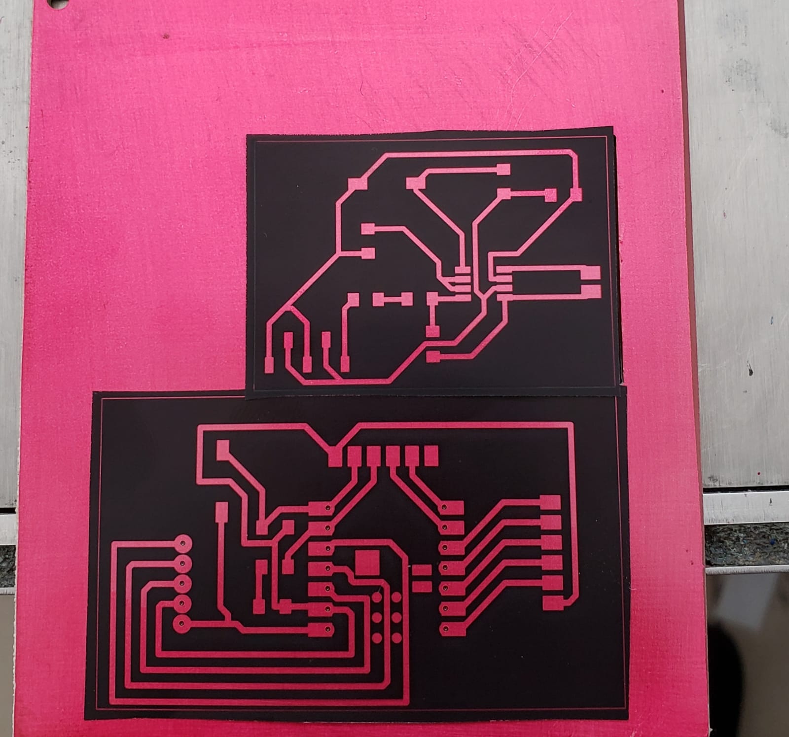
Once the mask was dry, I carefully positioned the negatives of each design over it, using the guide holes and side cuts for alignment. The board was then exposed to ultraviolet light, hardening the mask where exposed, while the covered areas remained soft and were later washed away with a potassium salt solution to reveal the design.
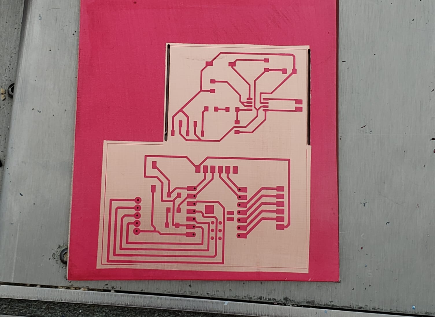
The final step involved removing excess copper using ferric chloride, which etches away the unwanted copper, leaving only the desired copper traces as defined by the hardened mask. This method ensured precision and fidelity to the original design, effectively transferring my digital design onto the physical board.
After that, our PCB was finally ready to be soldered!
However, the soldering process turned out to be my undoing. Despite my prior experience, the subpar solder I had bought led to a frustrating mess. The solder spread where it wasn't supposed to, creating shorts and risking damage to the Xiao module itself. The experience was disheartening, and for a moment, I feared that my entire project was compromised.
TRIGGER WARNING
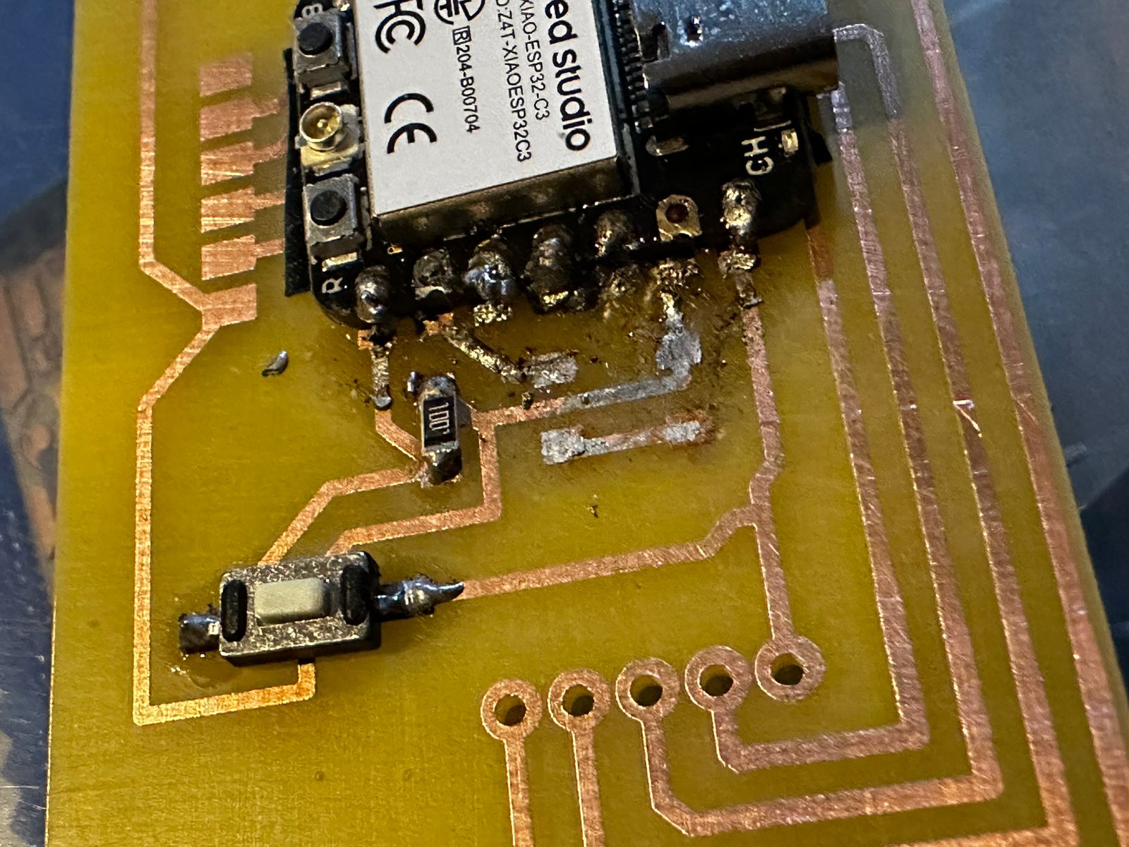
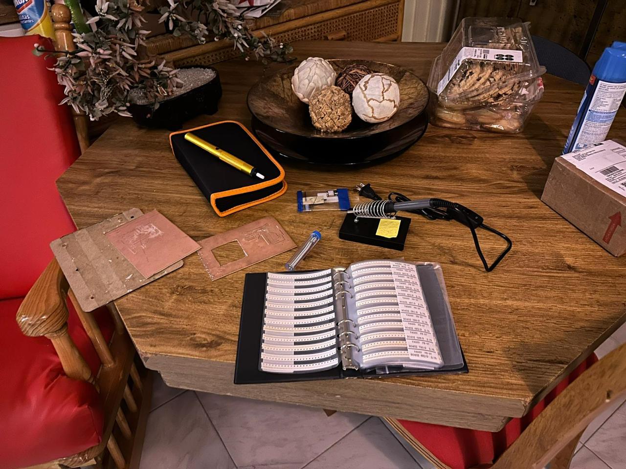
With this mess it was clear that I wasn't able to use this board anymore and I couldn't finish the assignment on time. After the soldering debacle, I had to learn to desolder quickly. Thankfully a friend of mine taught me what materials I should use to desolder quickly and efficiently without causing more damage that was already done. Here are the list of materials I used to desolder:


Using desoldering mesh that was submerged with Flux and applying heat with the Heat Gun and the Weller, I painstakingly removed the excess solder from the board. This process was new to me, and while challenging, it was also a valuable skill to acquire. Following this, I understood the importance of solder paste and its role in facilitating proper soldering.
However, I was able to save my, quite expensive, Xiao ESP32C3!
.jpeg)
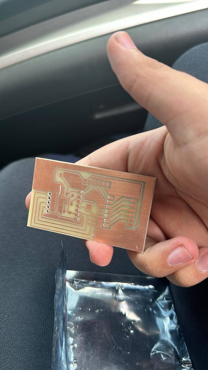
And here is what the board was like after cleaning everything up...
As you can see, it's beyond saving... there is solder everywhere!
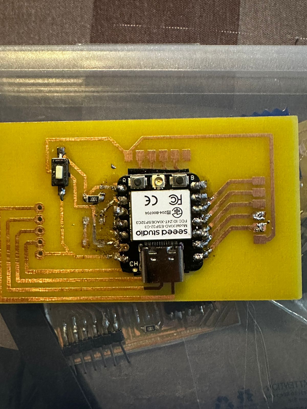
In order to fix this I remade the board completely and began by adding, as a safety measure, some female pins that will be able to hold the Xiao.
This way, if anything happens to the board, the Xiao will be safe and I can just take it out and place it again.
Next, I bought more expensive solder, and with that, I began the process to solder everything again.
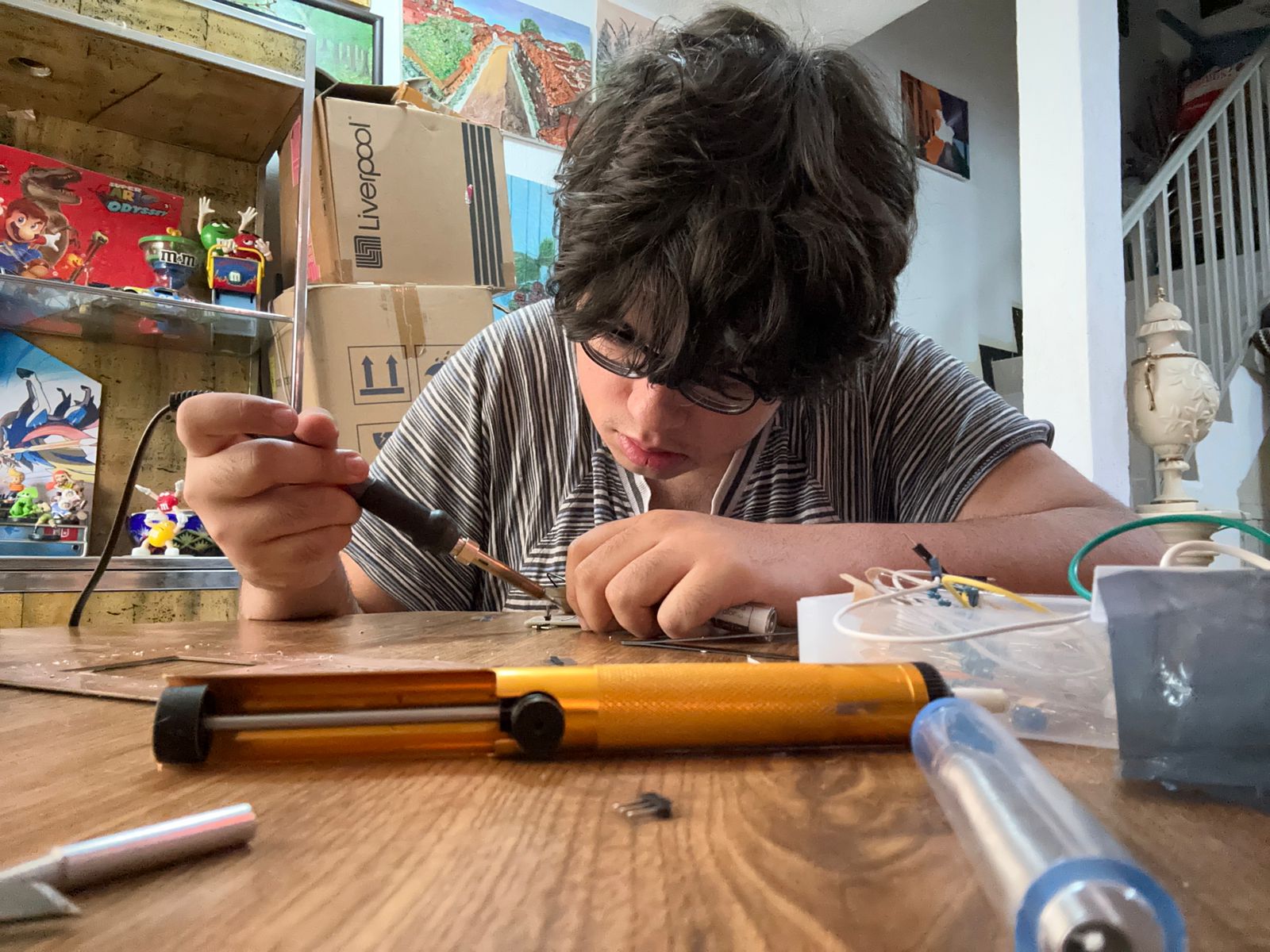
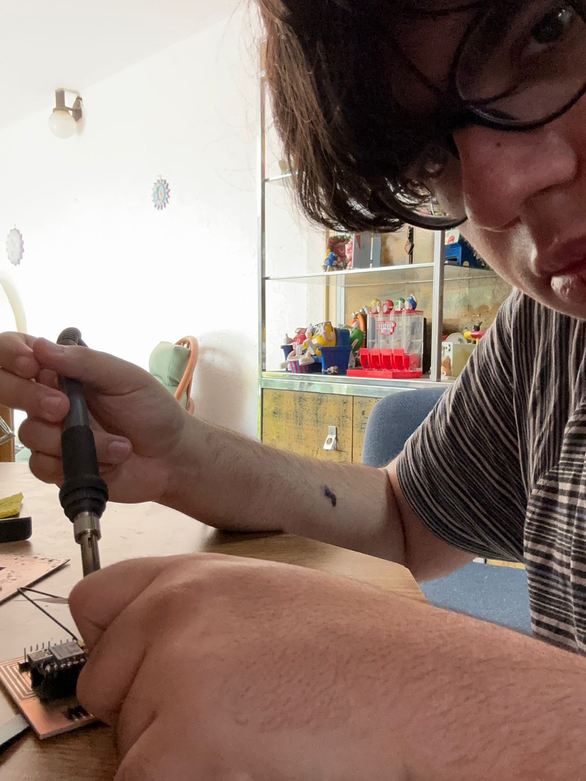
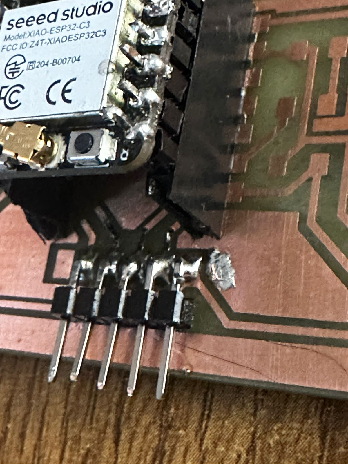
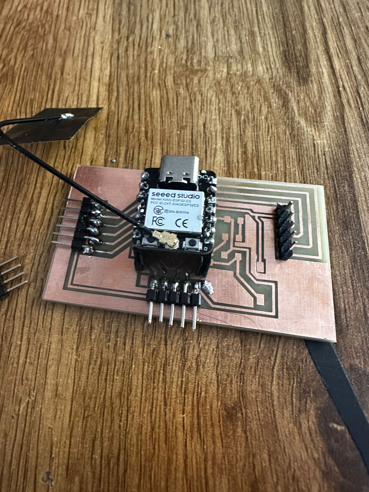
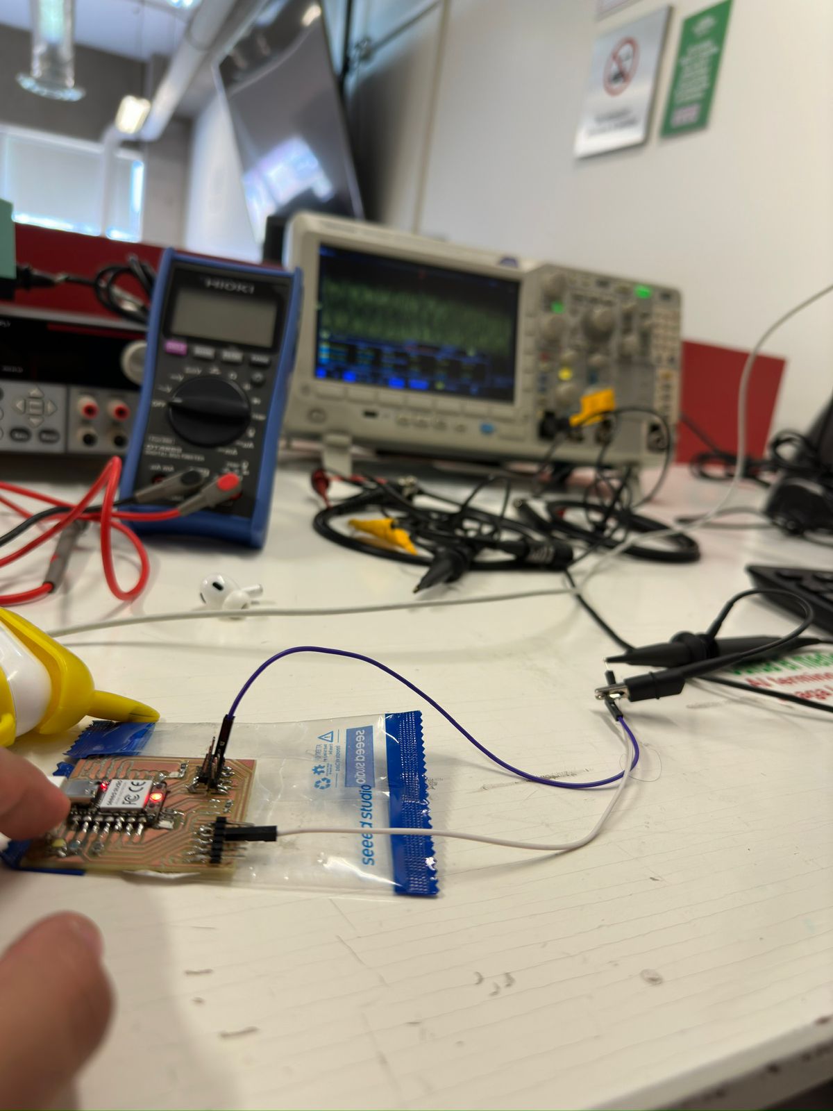
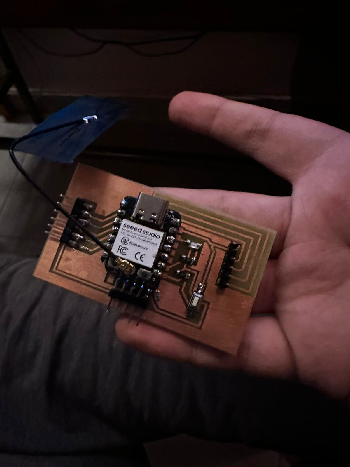
Here is the final result:
Finally, I used this code to check that everything is working via the button and the LED I implemented:
Xiao Esp32C3:
const int buttonPin = 0;  // Button pin
const int ledPin = 21;    // LED pin

void setup() {
  pinMode(buttonPin, INPUT_PULLUP);
  pinMode(ledPin, OUTPUT);
  digitalWrite(ledPin, LOW);

  // Define pin numbers
  const int buttonPin = 20; // D7
  const int ledPin = 8;    // D8

  void setup() {
	// Initialize the button pin as an input
	pinMode(buttonPin, INPUT);

	// Initialize the LED pin as an output
	pinMode(ledPin, OUTPUT);

	// Turn off the LED initially
	digitalWrite(ledPin, LOW);
  }

  void loop() {
	// Read the state of the button
	int buttonState = digitalRead(buttonPin);

	// If the button is pressed, turn on the LED
	if (buttonState == HIGH) {
	  digitalWrite(ledPin, HIGH);
	} else {
	  // Otherwise, turn off the LED
	  digitalWrite(ledPin, LOW);
	}
  }
And finally here is the PCB working correctly:
The Files:
Below you can find the download links for all of the files from this week.