I have never interacted with a PCB or anything like that (not even an Arduino) in my entire life. But you gotta start from somewhere... right?
PCB
What is a PCB?
A Printed Circuit Board (PCB) is an essential component in modern electronics, acting as a hub that connects various electronic parts through a network of conductive tracks, pads, and other features etched from copper sheets and laminated onto a non-conductive substrate. This construction facilitates the flow of electrical signals and power among the physical components of a device.
The PCB can be likened to a multilayered cake, composed of different materials bonded together with heat and adhesives, resulting in a unified, robust structure. This multilayered design is integral to its function and durability.

The substance of a PCB can comprise various materials, including FR1, FR2, FR3, FR4, etc., each offering distinct properties:
- FR1: This is a composite material featuring a thin copper layer atop a base of phenolic resin. Unlike the fiberglass-based FR-4, FR-1 is safer to handle, minimizing the risk of hazardous dust during milling. It is ideal for constructing circuit boards due to its ease of shaping and soldering.
- FR2: Also known as synthetic resin bonded paper, this material consists of paper impregnated with phenol formaldehyde resin, commonly used in PCB manufacturing.
- FR3: Similar to FR2, but utilizes an epoxy resin binder instead of phenolic resin.
- FR4: The most prevalent PCB material, FR4, is fiberglass-based, providing rigidity and durability to the PCB. This material is frequently used due to its balance of strength, cost, and insulating properties.
In Mexico, while FR1 is a healthier choice due to its safer handling properties, FR4 is more commonly found due to its affordability and widespread availability.
Further PCB layers and components include:
- Copper Layers: These are the foundational conductive layers. Depending on the complexity and cost constraints, a PCB may have copper on one or both sides and can range from one to over sixteen layers.
- Soldermask: This layer, usually colored (often green), lies above the copper layer. It insulates the copper tracks, preventing unintended electrical contact and aiding in precision soldering.

- Silkscreen: Silkscreen: Applied over the soldermask, this layer provides human-readable labels, symbols, and guidance, crucial for assembling and understanding the board's layout.

PCB terminology encompasses a variety of specific terms:
| Terminology | Description |
|---|---|
| Annular Ring: | The copper ring surrounding a plated hole in a PCB. |
| DRC (Design Rule Check): | Software-based verification of a PCB design to ensure error-free layouts. |
| Drill Hit: | Designated points for drilling holes on a PCB. |
| Finger: | Metal pads used for connecting two circuit boards. |
| Mouse Bites: | Perforated lines for easy separation of PCBs from a panel. |
| Pad: | Exposed metal on a PCB's surface for soldering components. |
| Panel: | An aggregation of multiple smaller PCBs for efficient manufacturing. |
| Paste Stencil: | A guide for applying solder paste in specific board areas. |
| Pick-and-Place: | A process or machine for placing components on a PCB. |
| Plane: | A continuous copper area on a PCB. |
| Plated Through Hole: | A hole that runs through the PCB, plated with metal. |
| Reflow: | The process of melting solder to form electrical connections. |
| Slot: | Non-circular holes, sometimes adding manufacturing complexity. |
| Solder Paste: | A mixture of solder and flux used in surface mounting. |
| Solder Pot: | A tool for hand soldering through-hole components. |
| Solder Jumper: | A tiny blob of solder connecting two adjacent points. |
| Surface Mount: | A method of mounting components directly on the PCB surface. |
| Thermal: | A trace connecting a pad to a plane, aiding soldering. |
| Thieving: | Copper patterns used to balance copper distribution during etching. |
| Trace: | The conductive paths on a PCB. |
| Wave Solder: | A method for soldering through-hole components on a PCB. |
Understanding these components and terms is crucial for anyone involved in electronics design, manufacturing, or repair, providing a foundation for effective communication and efficient work in the field of electronic engineering and PCB design.
Let's get soldering!
The Journey.
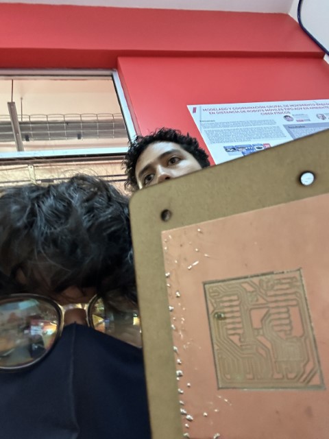
Embarking on the journey of mastering soldering at the FabAcademy class was a foray into uncharted territory for me. As someone completely new to the world of Printed Circuit Boards (PCBs), holding a PCB for the very first time was an experience filled with a mix of excitement and trepidation. The task at hand was to learn soldering, a skill that was as foreign to me as the PCB I held.
My initial encounter with the soldering station, set at a temperature of 360°C, was accompanied by a palpable sense of apprehension. The heat emanating from the soldering iron seemed daunting, and the thought of potentially burning myself loomed large in my mind, especially after our instructors' numerous safety warnings. These cautions were not just about the physical risks of burns but also about the potential damage to the sensitive electronic components that I was about to work with.
Despite these challenges, what followed was a journey of discovery and learning. I quickly realized that soldering required more than just technical skill – it demanded mental fortitude and a calm demeanor. The process of aligning the tiny components and melting the solder with precision called for a level of concentration and steadiness that I had not anticipated.
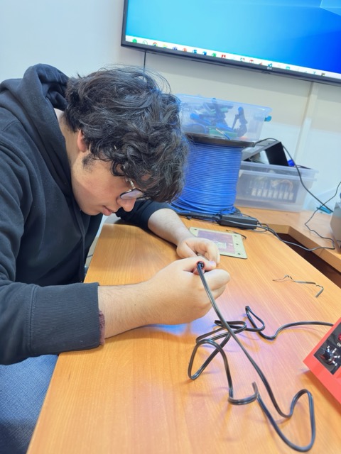

As I progressed, I found myself growing more confident, my initial fear of the heat and potential burns giving way to a focus on the task at hand. Each successful solder felt like a small victory, a testament to my growing skill and adaptability.
The experience was a blend of technical learning and personal growth. Not only was I learning how to solder, but I was also overcoming my apprehensions and learning to trust in my abilities. The accompanying photos capture this journey – from a tentative beginner to someone capable of handling the intricacies of surface mount soldering. This initial venture into the world of PCBs was not just about acquiring a new skill; it was about stepping out of my comfort zone and embracing the challenges of something entirely new and unfamiliar.

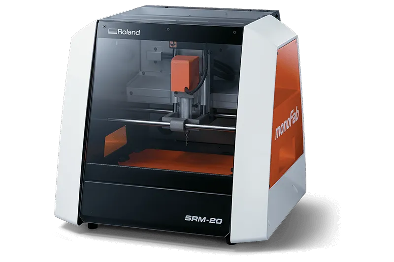
Milling Machine
The utilization of the ROLAND SRM-20 milling machine was a pivotal aspect of our PCB fabrication process in the FabAcademy class. This machine's versatility was evident in its ability to precisely mill a variety of materials, conforming to an array of formats and intricate specifications. The ROLAND SRM-20 is particularly adept at handling the delicate and precise requirements needed for creating detailed PCB designs. Its precision is paramount, as even the slightest deviation can lead to a malfunctioning circuit. This machine allowed us to experiment with different thicknesses and types of materials, giving us a hands-on understanding of how each variant impacts the final product.
Mini mills, functioning as CNC (Computer Numerical Control) machines, have distinct and easily identifiable components, each playing a crucial role in the milling process. Here's a closer look at these key parts:
- Front Cover: Serving as a critical safety feature, the front cover of the mini mill acts as a protective shield. It covers the front section of the machine, safeguarding the operator from flying debris and other hazards that might arise during the milling process. This barrier is essential in maintaining a safe distance between the user and the moving parts of the mill while it operates.
- (Power) Button: The power button is the primary control for activating or deactivating the mini mill. Positioned for easy access, this switch is crucial for starting the milling process and equally important for quickly turning off the machine in case of an emergency or upon completion of the milling task.
- Spindle Head: The spindle head is a dynamic component of the mini mill, containing the spindle motor. It plays a pivotal role in the milling process, as it is responsible for holding and spinning the milling tool. The movement of the spindle head in various directions allows for the precise shaping and carving of the PCB material according to the specified design.
- Working Table: The working table is the flat, stable surface on which the PCB material is placed and secured before milling begins. It is designed to move along different axes under the control of the CNC system, positioning the material precisely beneath the spindle head. This movement is critical for accurate milling, ensuring that each part of the PCB is machined as per the design specifications.
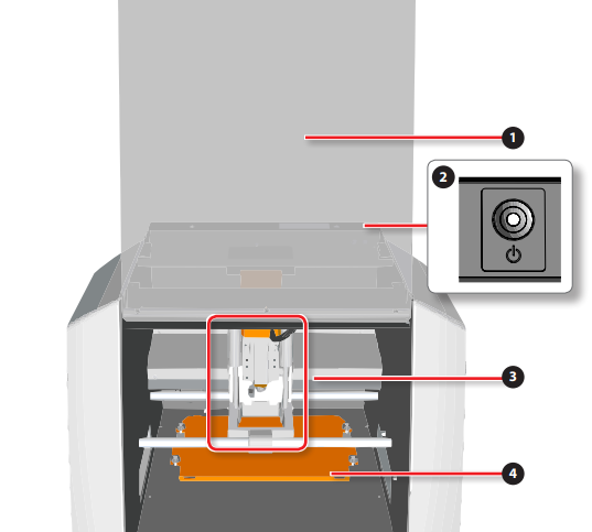
Each of these components works in harmony to enable the mini mill to perform intricate and precise milling tasks, crucial for the creation of detailed and accurate PCBs. The synergy of these parts, controlled by the CNC system, transforms digital designs into physical circuit boards with high precision and accuracy.
The ROLAND SRM-20 is a sophisticated and versatile mini mill, designed for precision milling of a variety of materials. Here's an overview of its key features and specifications:
- Cutable Materials: The SRM-20 is capable of handling a diverse range of materials, including modeling wax, chemical wood, foam, acrylic, polyacetal, acrylonitrile butadiene styrene (ABS), and printed circuit boards (PCBs). This versatility makes it suitable for a wide array of applications, from prototyping to educational purposes.
- Operational Travels in X, Y, and Z Axes: The machine offers a substantial range of movement, with operational travels of 203.2 mm (X-axis), 152.4 mm (Y-axis), and 60.5 mm (Z-axis). This range allows for the accommodation and precise milling of moderately sized workpieces.
- Loadable Workpiece Weight: The SRM-20 can handle workpieces weighing up to 2 kg, providing sufficient capacity for a variety of milling projects without compromising on precision.
- Operation Speed: The operational speed ranges from 6 mm/min to 1,800 mm/min, giving users the flexibility to adjust the speed based on the material being milled and the intricacy of the design.
- Software Resolution: The machine offers a software resolution of 0.01 mm/step when using RML-1 language and an even finer resolution of 0.001 mm/step for NC Code, ensuring highly accurate and detailed milling results.
- Mechanical Resolution: With an impressive mechanical resolution of 0.000998594 mm/step, the SRM-20 is capable of extremely precise movements, crucial for detailed and intricate milling tasks.
- Spindle Rotation Speed: The spindle speed is adjustable from 3,000 RPM to 7,000 RPM, allowing users to optimize the milling process for different materials and cutting requirements.
- Interface: The machine connects via USB, ensuring easy and reliable connectivity with most modern computers and control systems.
The ROLAND SRM-20 is thus a powerful and precise tool, ideal for a range of milling applications, from intricate PCB designs to detailed prototypes, offering both precision and versatility in a compact form. You can find more information in the Group Assignment.
The importance of adhering to specific formats and specifications cannot be overstated. Each material has its unique properties and requirements for milling, such as depth settings, milling speeds, and bit types. The ROLAND SRM-20's adaptability meant that we could fine-tune these parameters to match our specific design needs, ensuring that each PCB we produced met the highest standards of quality and functionality.
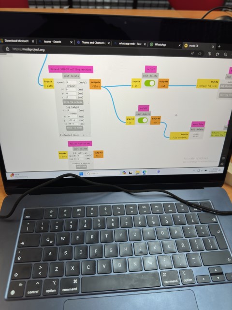
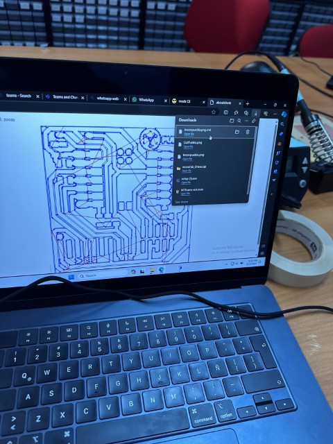
In addition to the physical milling process, the modsproject.org website played a critical role in our PCB design and fabrication workflow. This software was instrumental in translating our digital designs into precise instructions for the milling machine. It streamlined the process of setting up the milling paths, choosing the right tools, and determining the appropriate speeds and feeds for the material being used. This level of software support was crucial in avoiding common pitfalls in PCB fabrication, such as over or under-milling, which can lead to broken traces or incomplete cuts. As well as creating our .RML files ready for milling.
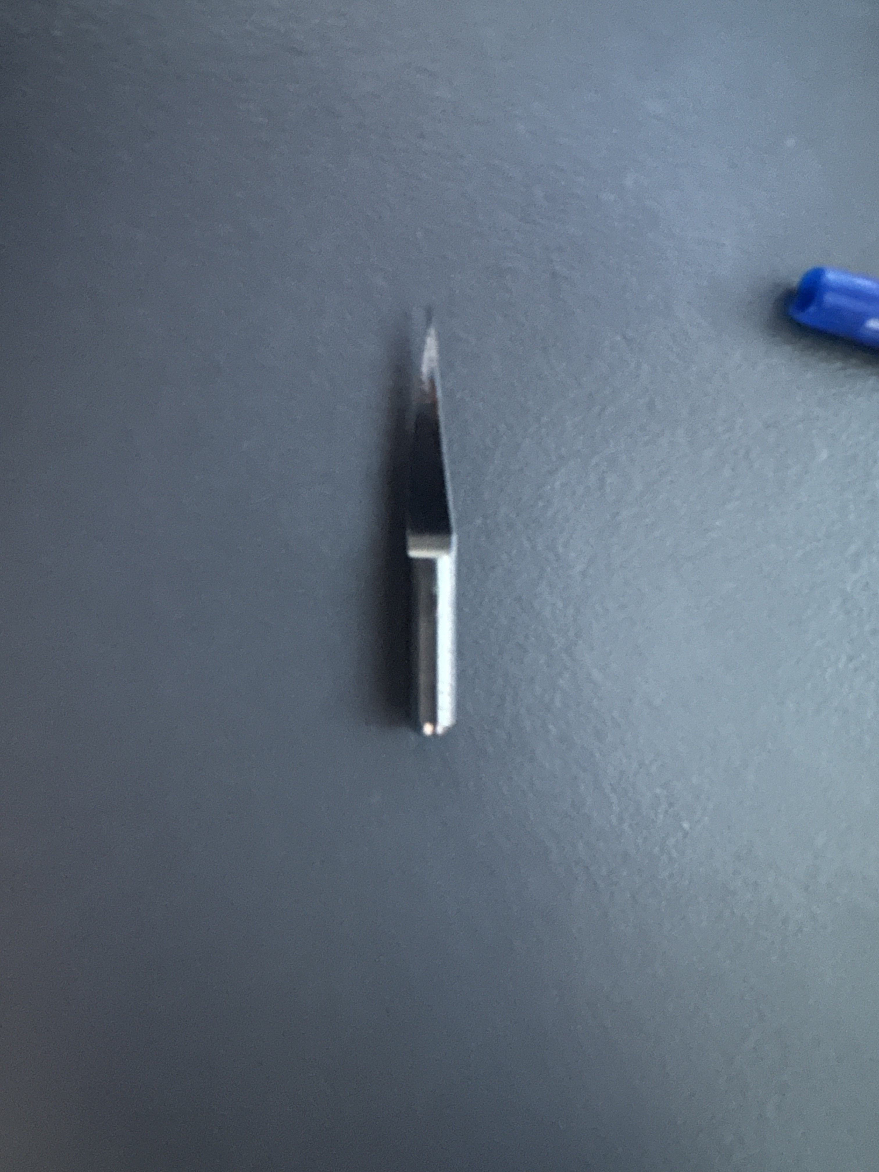
The "TIP" of the Iceberg.
When you need to engrave or cut a PCB using the ROLAND SRM-20, selecting and installing the appropriate tip is crucial. Start by removing the existing tip. This is done by gently loosening the screw with an Allen key. To prevent any damage to the tip, such as flattening from a fall, place a sponge underneath it for a safe and cushioned landing.
The engraving tip we used:
Once the tip is changed, it's time to configure the machine for engraving. This involves adjusting specific parameters on the machine's control panel. A key parameter to focus on is the offset. In our case, we experimented with an offset value of 4. This adjustment helps to widen the tracks, making the soldering process more manageable.
Loading the .RML file into the machine is the next step. Begin by powering on the machine using the power button. Then, carefully install the new engraving tip, ensuring it is properly adjusted. To accurately position the tip, use the 'view' button, which moves the tip to the 0,0 coordinate. Further fine-tune its position along the Z-axis using the UP and DOWN buttons for precise placement.
The setup for engraving requires a few additional steps. Open the RolandMDX_20ControlPanelCode software on your computer. The tip should then be adjusted to just touch the surface of the PCB. A practical way to determine this is by placing a sheet of paper under the tip and lowering it gradually. When the tip slightly tears the paper, it indicates the correct height for engraving. Next, in the software, set the origin coordinates for both X and Y.
Finally, you're ready to start the engraving process. Load your .RML file into the software, and the machine will begin the detailed task of etching your design onto the PCB. This process requires precision, and by carefully setting up the machine and configuring the software, you can achieve high-quality engravings that align with your design needs.
The engraving process
Loading our .RML file
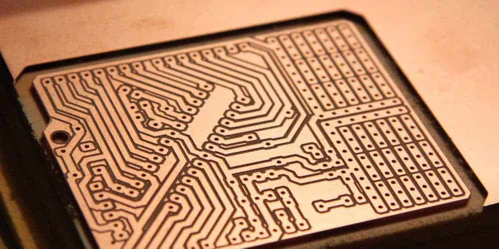
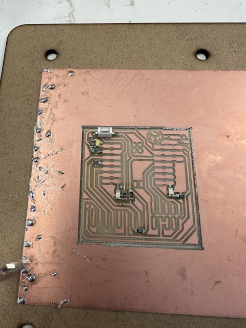
Using the ROLAND SRM-20 for milling PCBs was an intricate process, which involved both preparing the design files and understanding the machine's operation. My experience began with creating the design for the PCB, for which I used the modsproject.org website. This platform was instrumental in converting my PCB design into a format suitable for the milling machine. The website's user-friendly interface allowed me to input my design and tweak various parameters, ensuring that the output file would be precisely aligned with the capabilities of the ROLAND SRM-20.

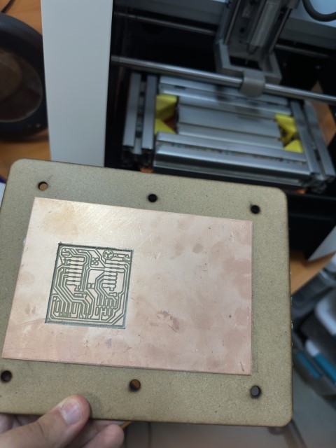
Once my design was ready and converted into the appropriate format, the next step was to set up the milling machine. For this project, I was working with copper, known for its excellent conductivity and durability in PCB applications. However, milling copper presented its own set of challenges. One crucial aspect was the use of double-sided adhesive tape. This tape was necessary to secure the copper sheet onto what we referred to as the "sacrifice bed."
The sacrifice bed is a layer placed on the milling machine's platform to protect it from any potential damage during the milling process. The adhesive tape ensured that the copper sheet remained firmly in place, preventing any movement that could result in inaccuracies or damage to either the copper sheet or the machine.

Operating the ROLAND SRM-20 was a lesson in precision and careful control. After loading the design file into the machine, I carefully monitored the milling process, making minor adjustments as needed. The spindle of the machine whirred into action, meticulously carving out the design onto the copper sheet. It was fascinating to watch the machine translate my digital design into a physical PCB, with each pass of the milling head revealing more of the intricate circuit pathways.

Throughout this process, I was constantly aware of the importance of accuracy and attention to detail. A slight misalignment or incorrect setting could result in a flawed PCB, rendering it unusable. However, the satisfaction of seeing the finished PCB, exactly as I had designed it, was immensely rewarding. It was a testament to the precision of the ROLAND SRM-20 and the effectiveness of using modsproject.org for preparing the milling files. This experience not only enhanced my understanding of PCB fabrication but also deepened my appreciation for the meticulous nature of working with such advanced machinery.
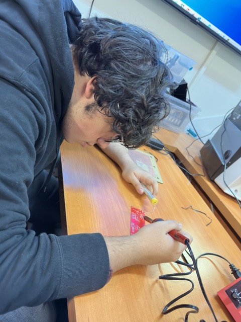
The soldering process
Here comes the toxic smoke!
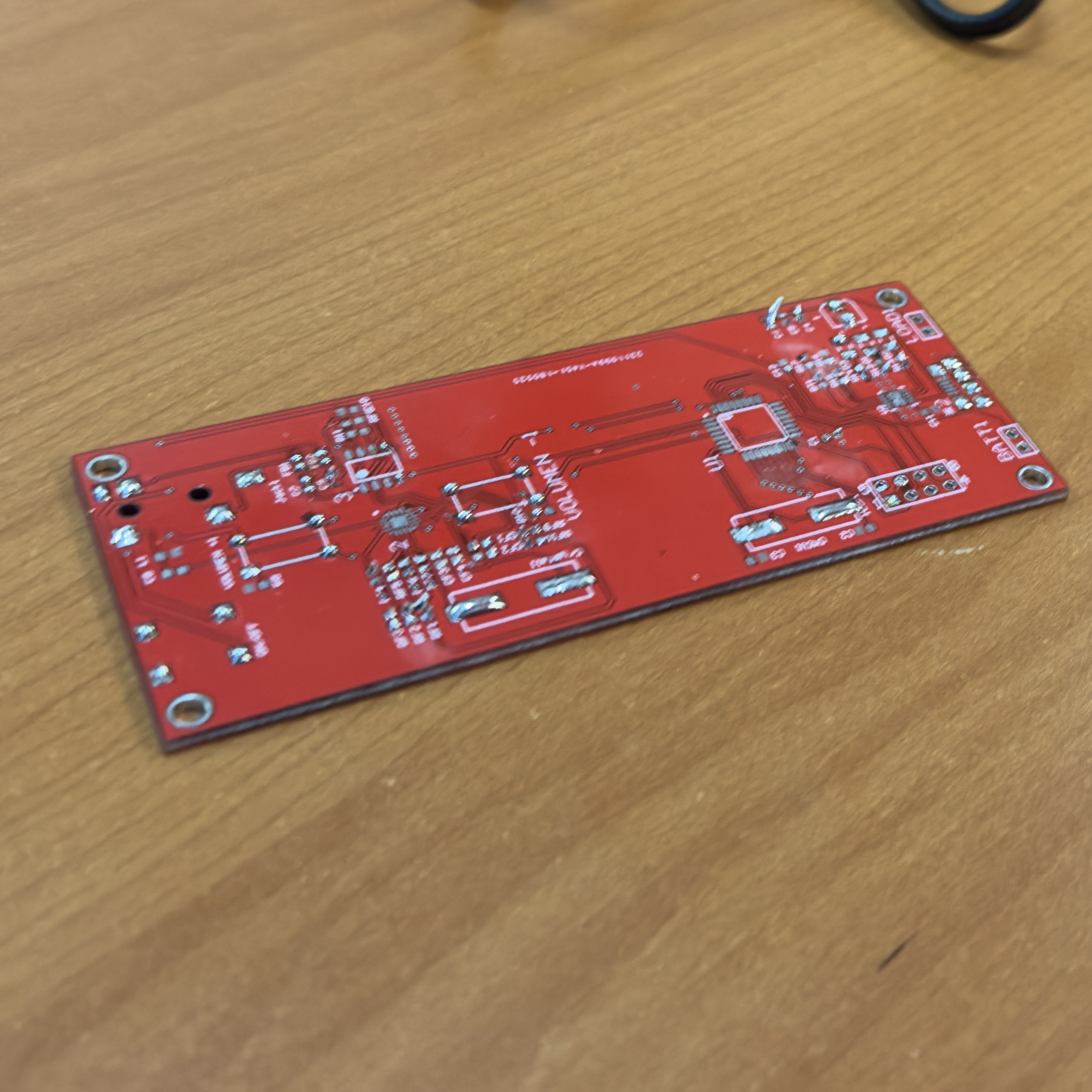
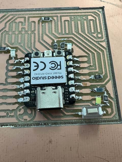
The soldering process for the PCB I worked on began once I had the milled board ready. It's a methodical process that requires a good deal of precision and patience, especially when dealing with the tiny components and fine traces that you can see in the images provided.
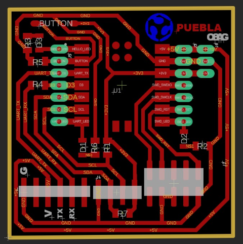

The first step was to carefully inspect the milled PCB for any irregularities. I needed to ensure that all traces were intact and that there were no unwanted connections that could lead to shorts. This step is crucial because any errors not caught here could cause problems down the line after soldering is complete.
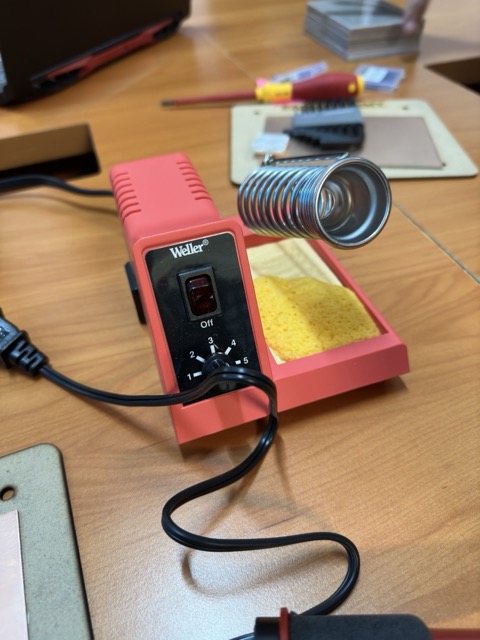
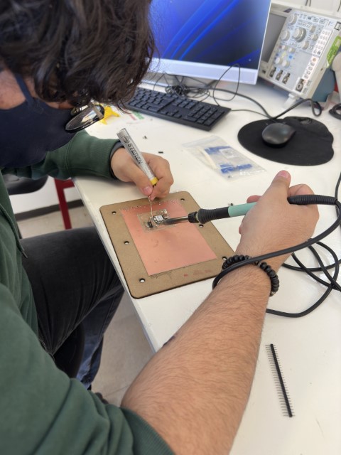
Next, I prepared my soldering station, setting it to the correct temperature for the solder I was using. The solder needs to melt smoothly to form good joints but not so hot as to damage the components or the PCB, the ideal temperature was 360°C. I placed the board onto a stable, heat-resistant surface to begin the work.
Then, I needed to get the following materials:
| Material | Quantity |
|---|---|
| 1.1Ω Resistances: | x5. |
| 2.0Ω Resistances: | x1. |
| Light-emitting diode: | x3. |
| XIAO RP2040: | x1. |
| 90° Pins: | x10. |
| Pins: | x5. |
| Button: | x1. |
With all the components organized and at hand, I started by tacking down all the small components so I wouldn't get lost.
For these smaller components, such as resistors and capacitors, I used a fine-tip soldering iron and sometimes a magnifying glass to see the work area better. The key here was to apply just the right amount of solder – too much could create bridges between adjacent pins, and too little might result in a cold joint, which could cause circuit failure.
I proceeded to solder the button. I paid close attention to its placement, making sure that it was firmly attached and that its connections were solid, as this would be a key interactive element in my project.
During the process, I also had to be mindful of the heat transfer. Some components are sensitive to heat, so I needed to work quickly to avoid damaging them. For components with many pins, such as microcontrollers or connectors, I often used the technique of adding a small amount of solder to one pin to hold the component in place. Then, I would solder the opposite pin to secure the component before soldering the remaining pins.
After this I soldered the Xiao RP2040 microcontroller onto the board. To ensure the safety of the components and prevent any potential short circuits, I applied insulation tape to the bottom of the Xiao. This was a crucial step because the microcontroller's underside could otherwise come into contact with the metallic traces or parts on the PCB, leading to electrical shorts.

Once the hardware was in place and checked for any soldering errors.
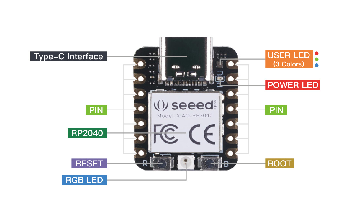
I moved on to programming the Xiao RP2040. But first I needed to learn how the Xiao worked through this diagram and through this tutorial made by seeed studio.
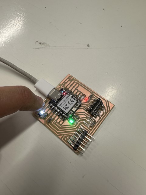
Writing the code to control the LEDs was an iterative process. I began with a simple blinking program for the bottom LEDs to ensure the basic functionality was intact. Then, I expanded the code to include the button interaction. By pressing the button, an interrupt signal was triggered, causing the LED on the top part to flicker, which confirmed that both the input (the button press) and output (the LED flicker) were functioning as expected on my freshly assembled PCB.
The code:
However, when I first uploaded my code to the Xiao RP2040, none of the LEDs lit up, which was quite alarming. It left me puzzling over where the fault might lie – was it in my soldering, the code, or the components themselves? To troubleshoot, I meticulously reworked the solder joints on the resistors and LEDs, ensuring they were solid and there was no excess solder that could cause shorts.

This careful revision paid off, and after cleaning up the excess solder and reinforcing the connections, the LEDs began to function as intended, much to my relief. It was a valuable lesson in the importance of precise soldering and thorough inspection when working on PCBs.
Video of the PCB working correctly through the Xiao code:
Finally I solded the 90° pins and horizontal pins. Once all the components were soldered onto the board, I inspected my work for any solder bridges or poor joints and corrected them as needed.
The final step was to remove the PCB from its base and testing the board again to ensure that all connections were solid and that the board functioned as intended and to check that I hadn't moved anything when solding the pins. It was always rewarding to power up the finalized board for the first time and see the components come to life, indicating a successful soldering job.
Conclusion
In conclusion, the journey from soldering the initial components to debugging and programming the Xiao RP2040 was both challenging and rewarding. The initial scare when the LEDs failed to light up served as a stark reminder of the attention to detail required in electronics. It pushed me to revisit my work, refining the soldering connections and ensuring there was no excess solder that could compromise the circuit's functionality. This hands-on experience not only bolstered my technical skills but also provided a deeper appreciation for the meticulous nature of PCB assembly and the thrill of problem-solving in the world of embedded systems.
Now that my PCB project is complete, I can finally breathe easy – and not just a sigh of relief. No more personal daily specials of solder smoke aromas for me. It's back to fresh air... until the next soldering adventure, that is!
The Files:
Below you can find the download links for all of the files from this week.