8. Electronics Design
This week I had to design a board, whose purpose was to interact and communicate with a microcontroller. I only decided the microcontroller that I'd be using for my final project, because next week is the one to know about outputs. For this task I put pinheaders to all of the pins from the board (Xiao ESP32-C3) so that I would be able to use them in my final project.
Group Page
In this week's group page there is information about testing and observing the functionality of a board, as well as information of what's required to send a PCB to a board house. The tests and functionality of a board can be shown using the multimeter and the oscilloscope.
Multimeter
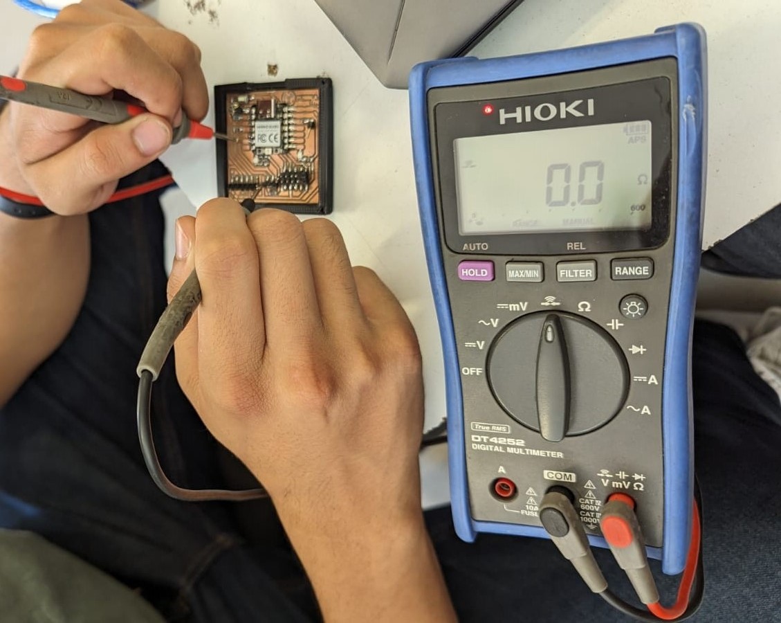
The multimeter is a device used to make different measurements about the different characteristics of a board, such as voltage, continuity, resistance, capacitance, current, and test diodes. For each measure there is a mode using the knob in the multimeter to select it. The measurements shown by the instructors are the following (which are the basics to know how a board is working and if it is working as expected):
- Continuity (icon shown below): it verifies that all the paths that are expected to be connected, are indeed connected. During this test, when there is continuity, the multimeter turns on its red light, marks low resistance and makes a sound (a little bip).
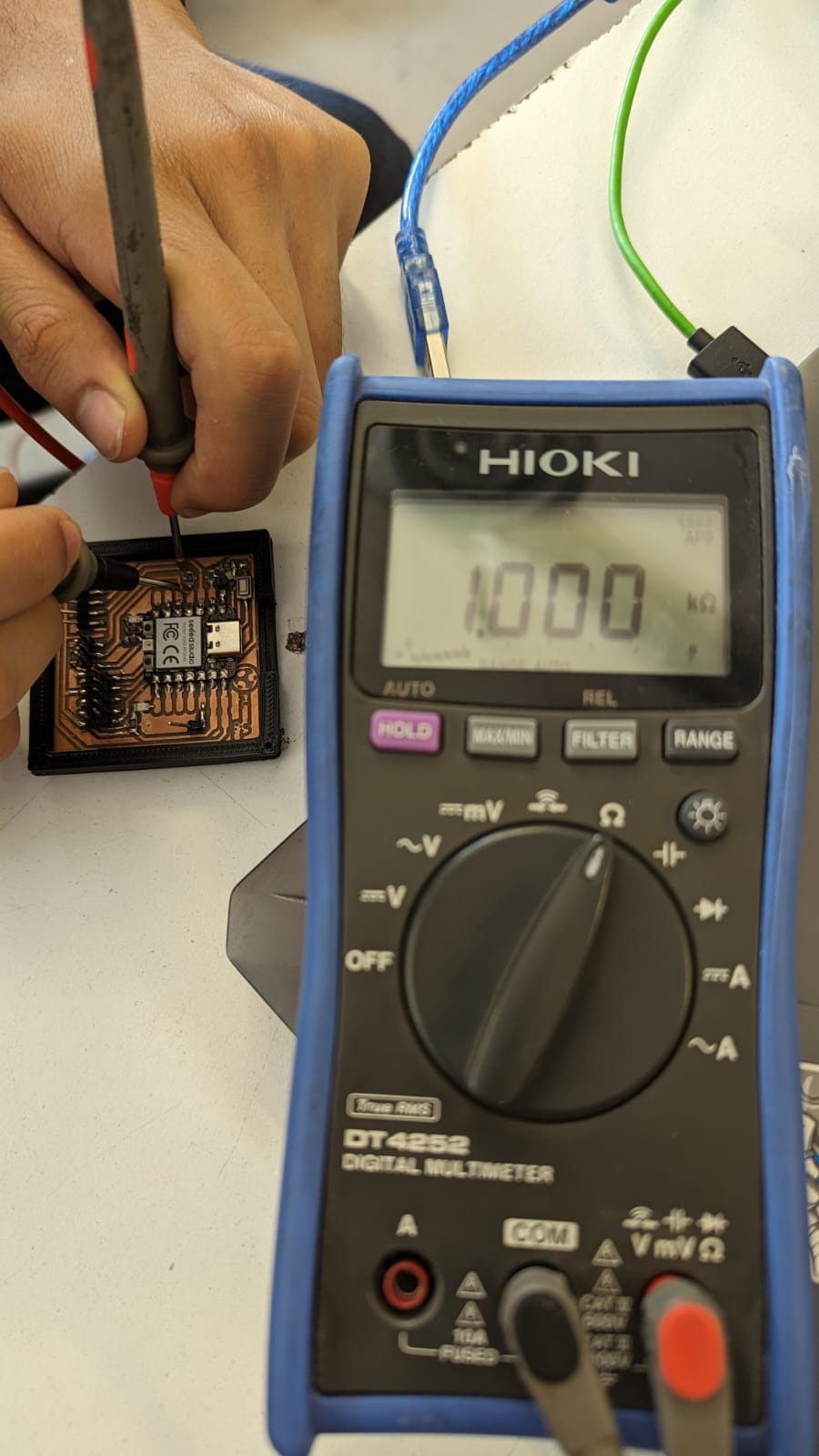
- Resistance (icon shown below): it measures the value of the resistors. In the second picture it gives a value of 1 kΩ, as it should be.
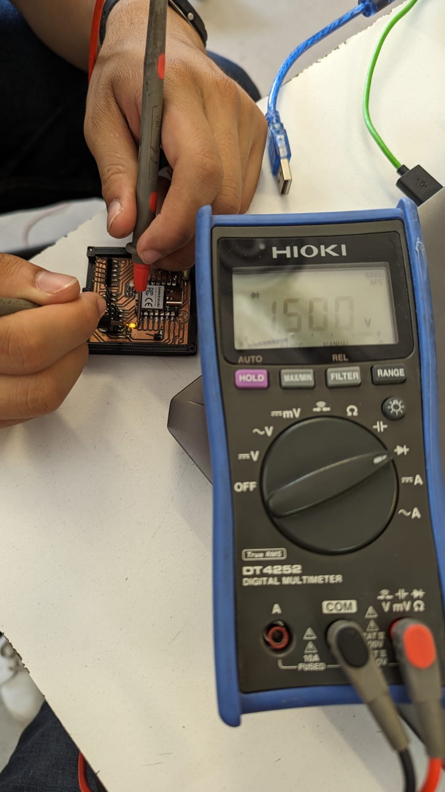
- Diode Tester (icon shown below): the multimeter provides the voltage and, if the test leads, are connected correctly, the LED will turn on (as shown in the second picture). This shows that the LED is soldered properly and is working well.
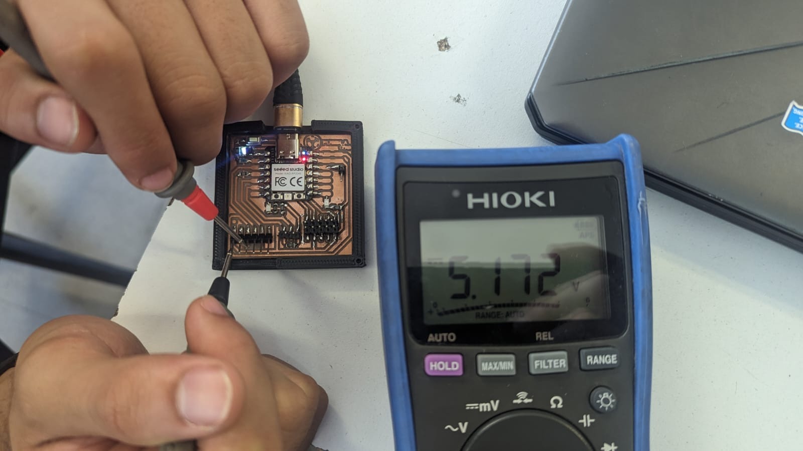
- Voltage (icon shown below): for this test it is necessary to place the black test lead to GND and the red one to the aim pin (as in the second picture). This will give the value of the voltage given by the powered pin.


Oscilloscope
In order to use the oscilloscope, it is necessary to connect the oscilloscope tips to any of its two channels. Then, place the black probe to GND and the red one to the signal we want to read:
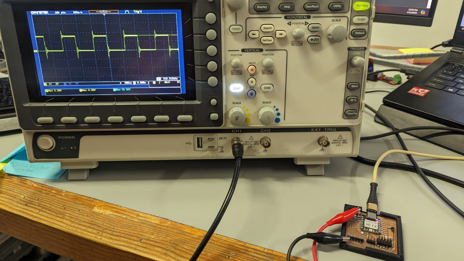
The oscilloscope will show the signal in the display as a graph through time, which would be how the signal varies. This is useful to know if the code is functioning correctly and sending what it is supposed to send.
Send PCB to Board House
It is possible to create a PCB by our own (hence week 4), but one may also send it to a board house to be manufactured. For this the only necessary thing is the gerber file. A gerber file has the information of all the layers involved in a PCB (copper layers, the soldermask layer, the sikscreen layer, the mechanical dimension and the drill location). So the steps to follow are the next ones:
- Get gerber file.
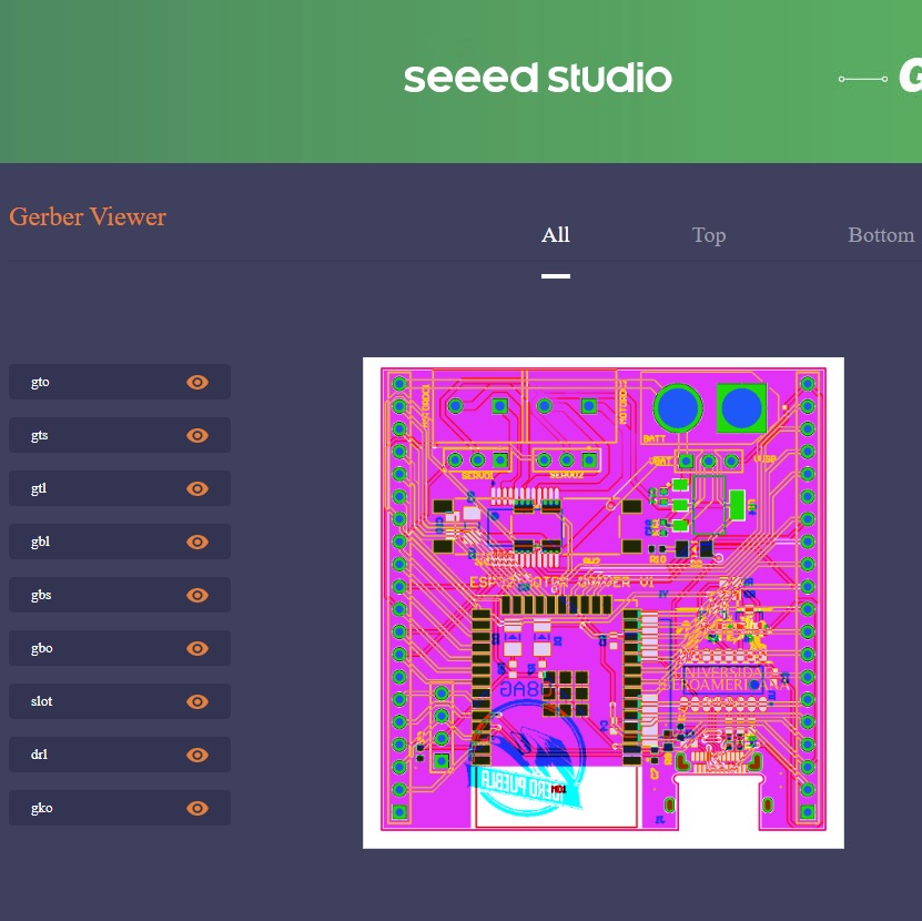
- Upload gerber file to a gerber viewer to see if everything is correct.
- Upload file to a fabhouse (in the case of FabLab Puebla, we use FUSION from SEED Studio):
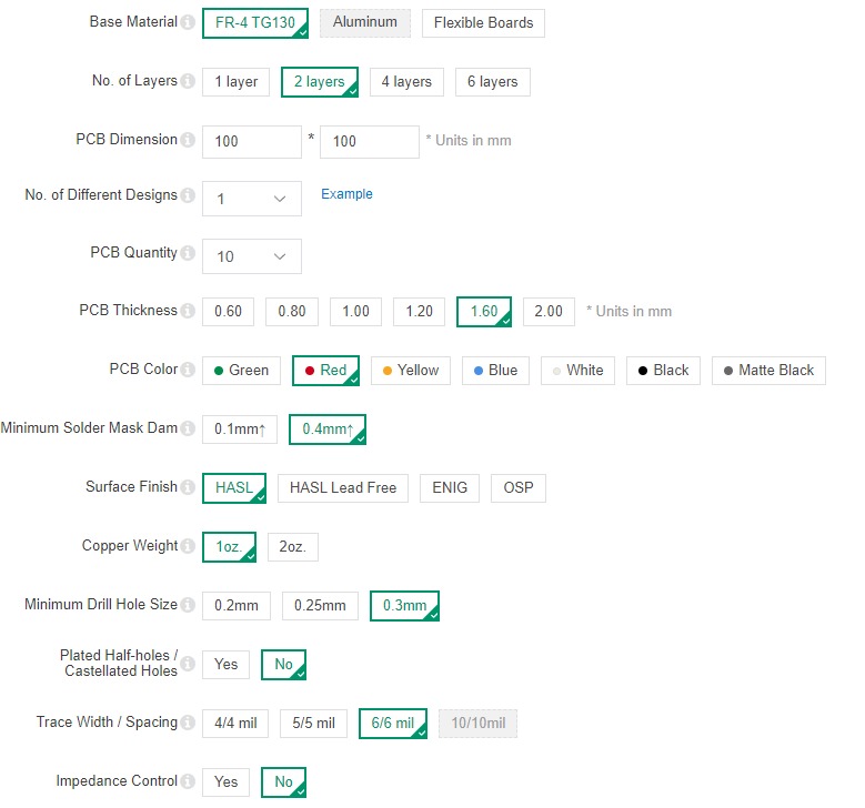
- Choose the parameters of the PCB:
- Wait for delivery.
- Solder components.
Designing the PCB
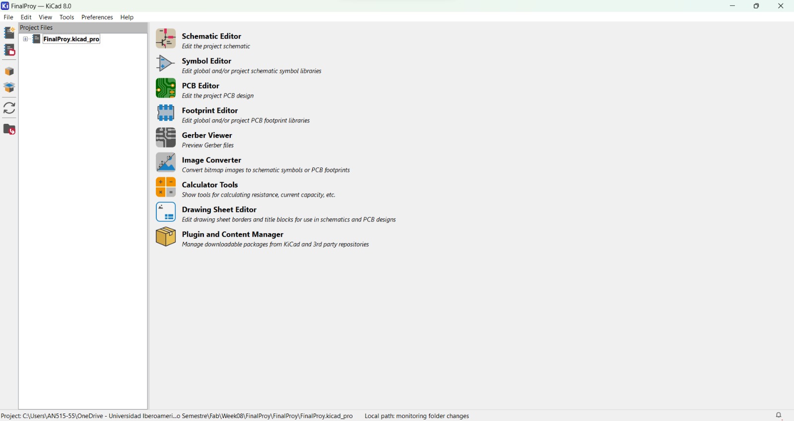
To design the PCB there are many different softwares, such as KiCad, Eagle, Altium, and EasyEDA. For FabLab Puebla it was easier to use KiCad since it is a free software and it doesn't requires any license; also it allows personalized libraries for the components. The software looks like this:
Import Libraries
First of all, I had to import the libraries of the components available in FabLab Puebla, so that I'd be sure that the components are available. What needs to be imported to have the personalized libraries in KiCad are the components' symbols library, the components' footprints library, and the 3D design of the components.The steps to import the libraries are the following:
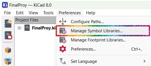
- First, I imported the symbol libraries by clicking in Preferences, and then clicking in Manage Symbol
Libraries....
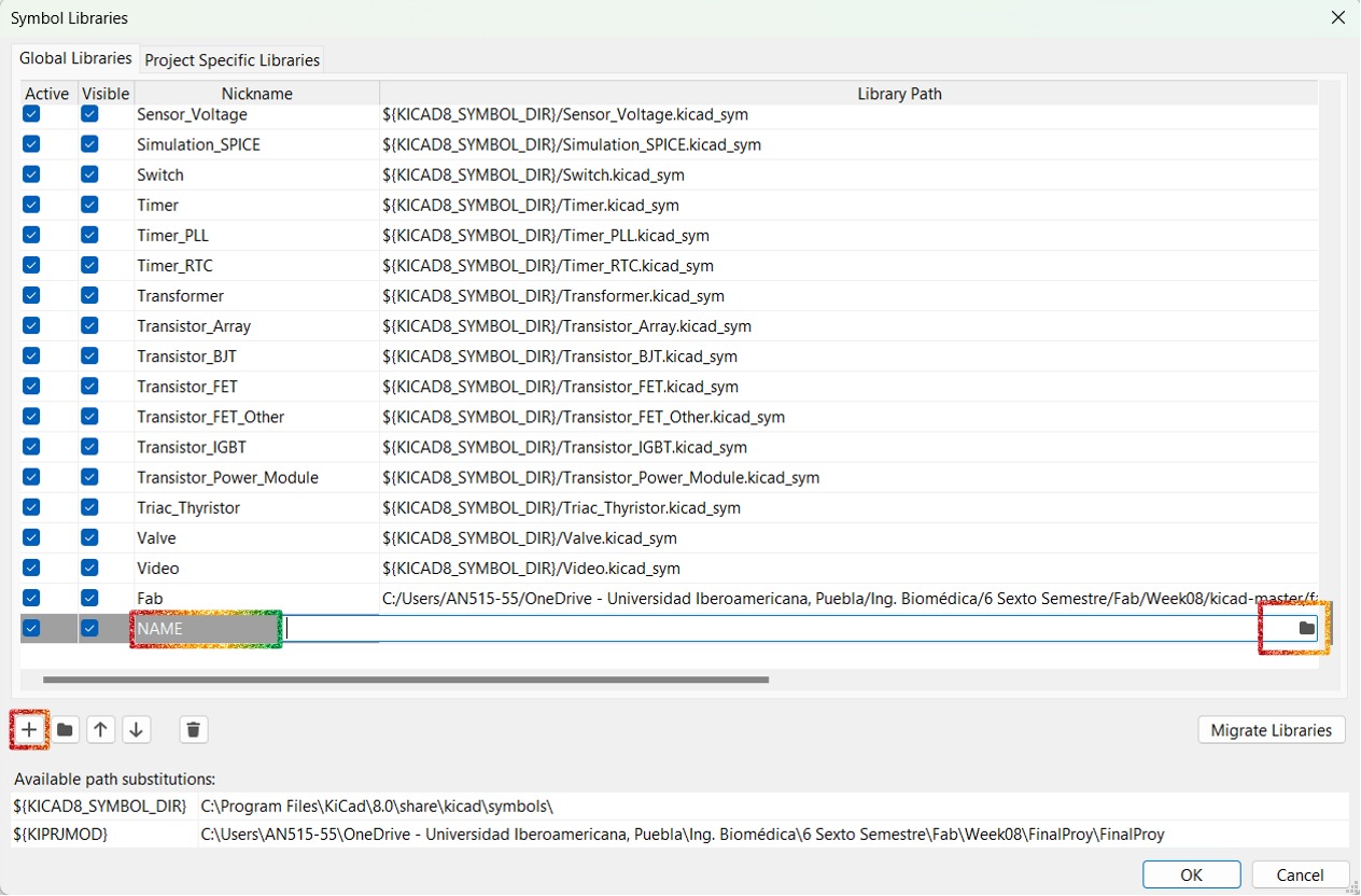
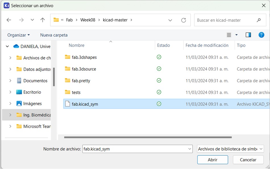
- Then add a new library, name it, and select the file where the symbols are (second picture).
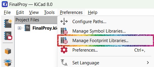
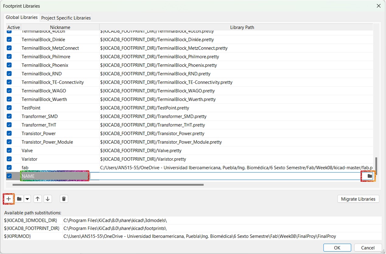
- Secondly, I imported the footprints of the components by following a similar procedure: click in Preferences,
then click in Manage Footprint Libraries....
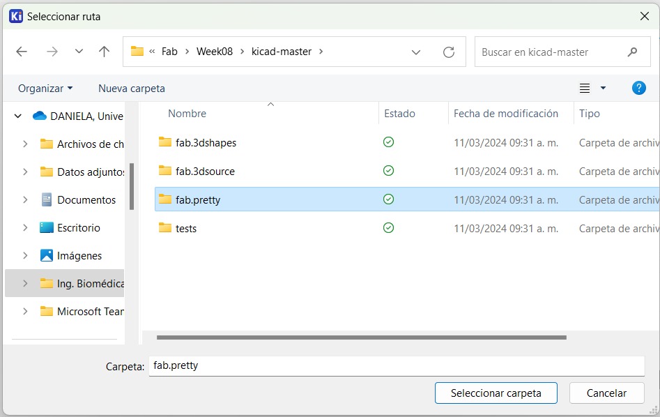
- Then add a new library, give it a name, and select the file were the footprints are (second picture).
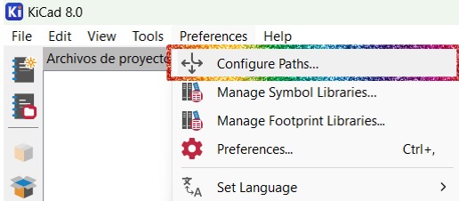
- Finally, to add the 3D designs of the components click in Preferences, and then in Configure Paths....
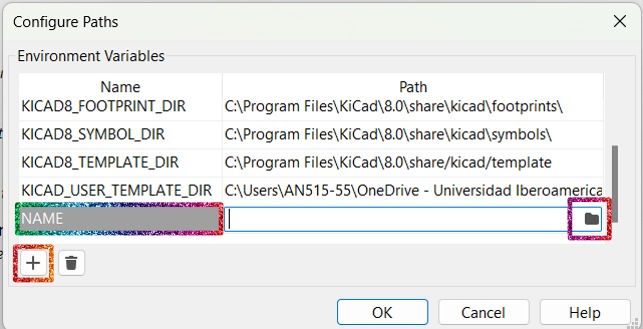
- Then add a new library for the paths, name it, and select the whole folder where all the files of the library are
(second picture).
Schematic Design
To create the schematic file, there aren't exactly steps to follow in order to design the circuit, but there are some steps to do the file:
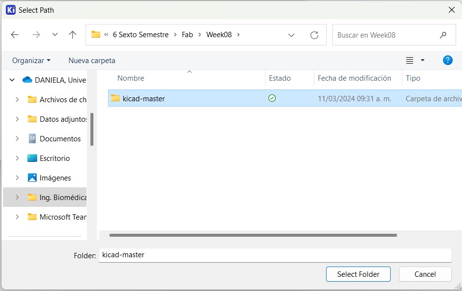
- To create the schematic design I first had to create a new project to work with:
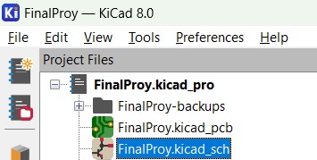
- Then double click on the schematic file of the project:
- Add the necessary symbols to create the schematic of the circuit. First click in the next icon (located in the
right bar of the interface):

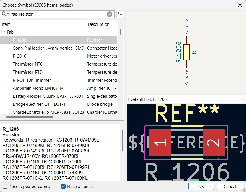
- There I chose the symbols needed for the circuit, as well as there I could also observe the footprint of each
component in order to know whether or not it has the characteristics I need. The components I needed were:
• 1 Module XIAO ESP32C3
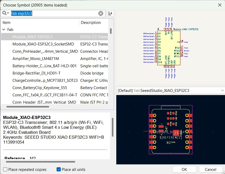
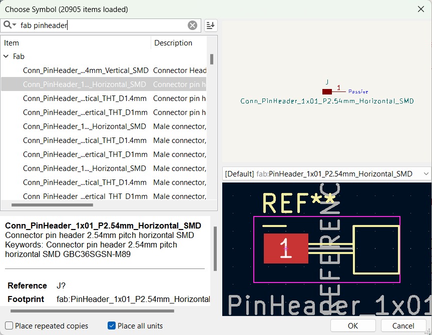
• 2 Pinheaders 1x1
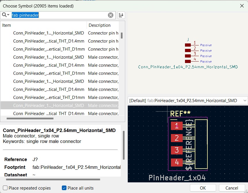
• 3 Pinheaders 1x4
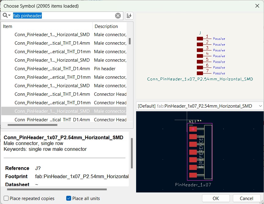
• 1 Pinheader 1x7
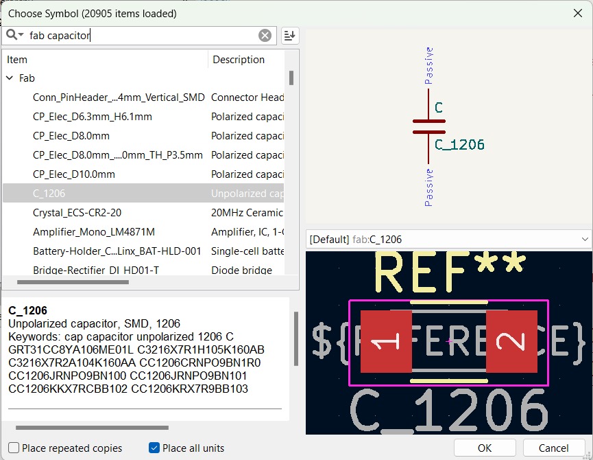
• 1 Capacitor (1 μF)
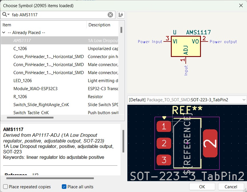
• 1 Regulator AMS1117
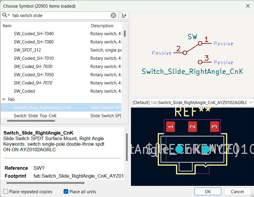
• 1 Switch
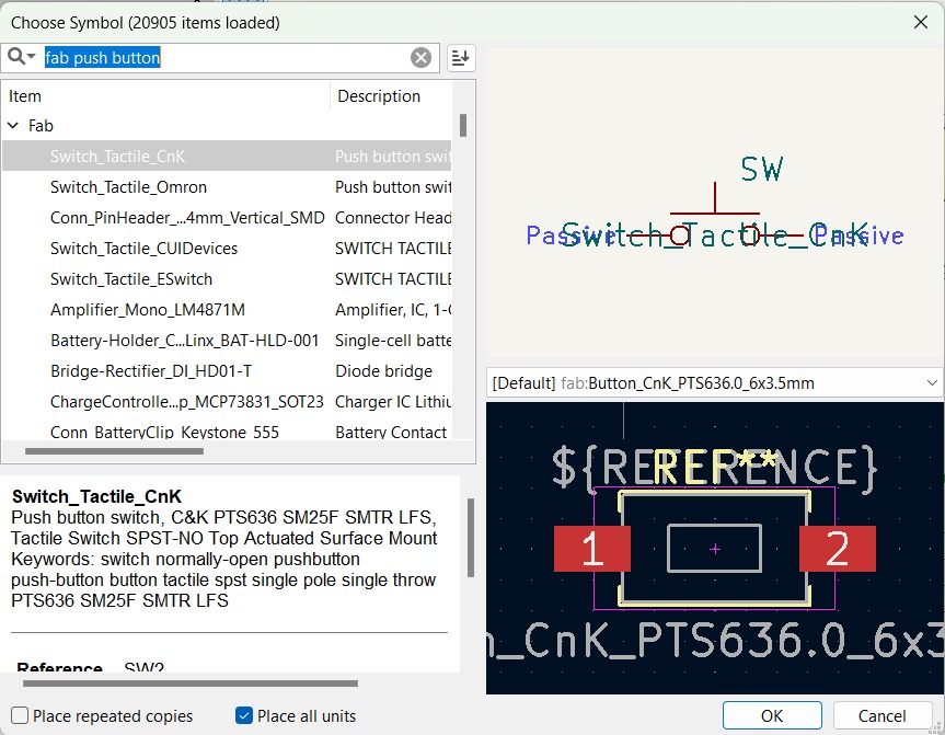
• 2 Push Buttons
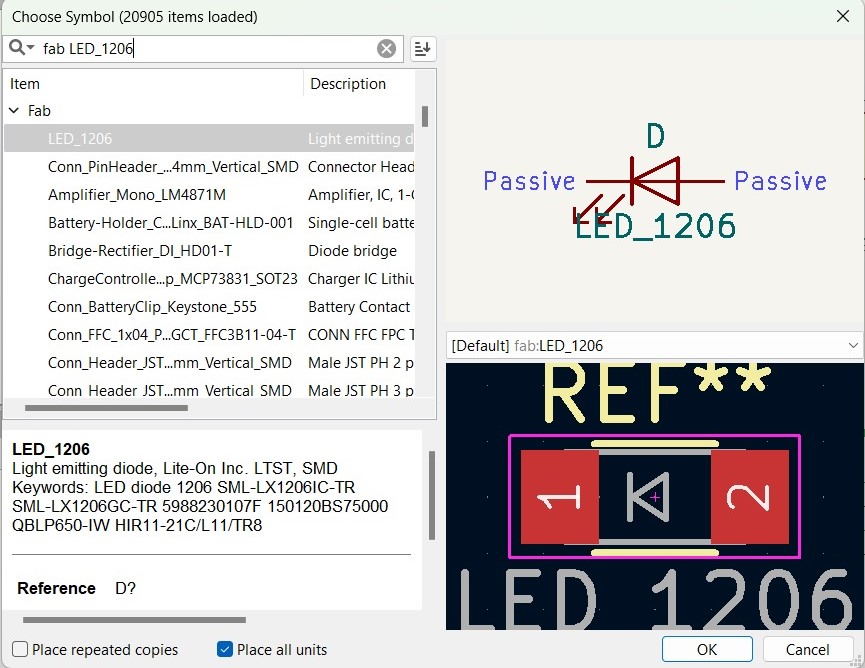
• 4 LEDs
• 6 Resistors
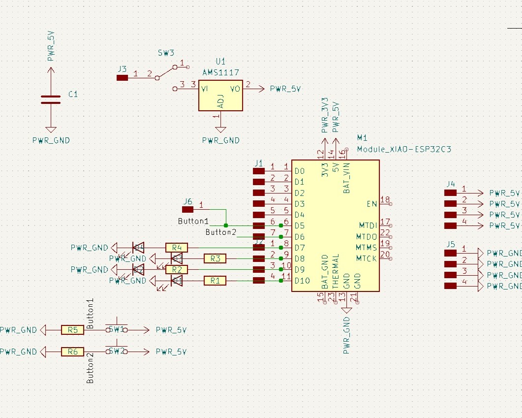
- The connections between the components are done by clicking on the end of the component and drawing the line as you want
to go. However, there is also a tool to tag the connections of the components and avoid a bunch of cables (which is also
located in the right bar).

- The final schematic ended as the following picture:
PCB Design
To design the PCB there aren't such as steps to follow, but there are some things to do in order to edit it:
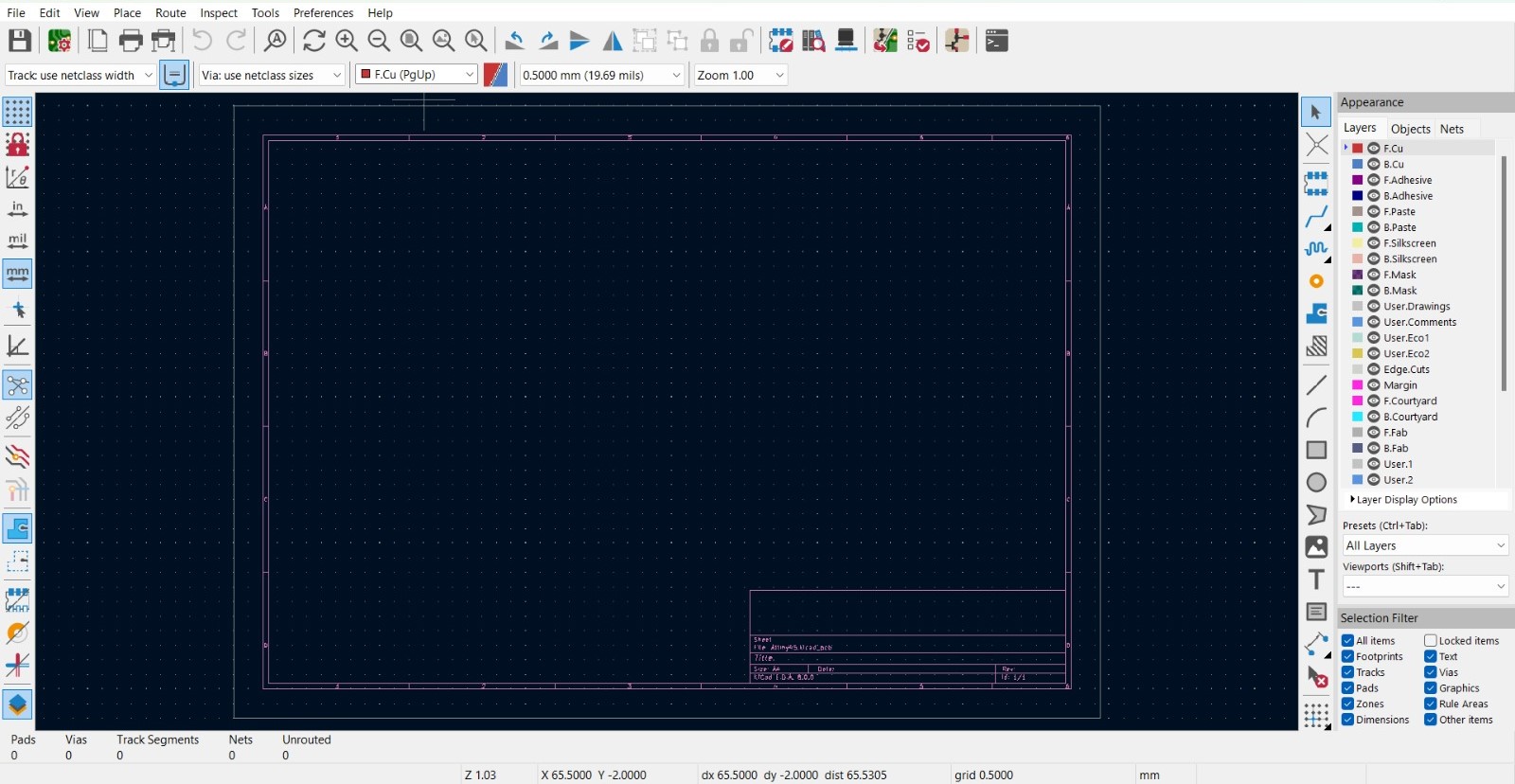
- Click in Open PCB in board editor (an icon in the upper bar).

- So it opens the next window:
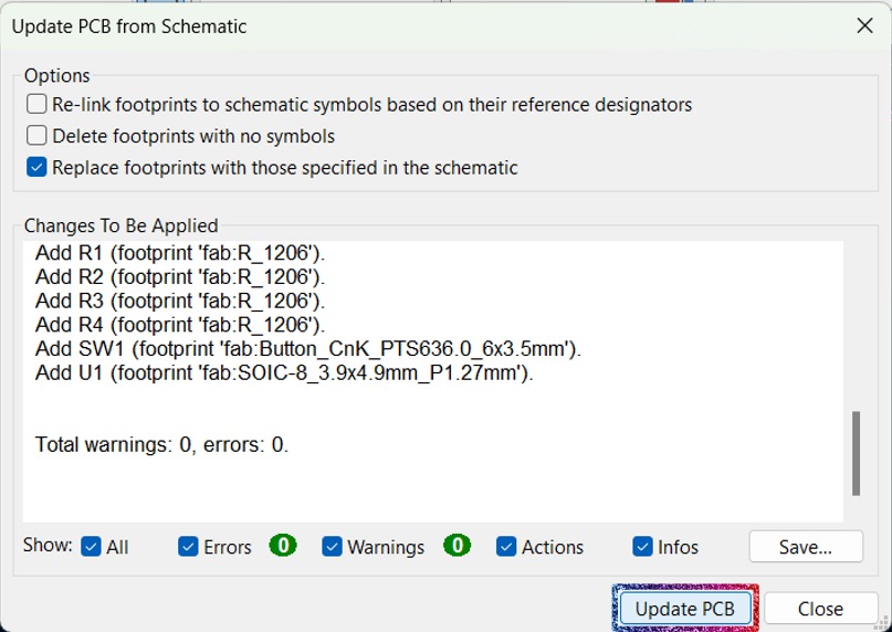
- Then I brought the components by going to Tools, and then click in Update PCB from Schematic.
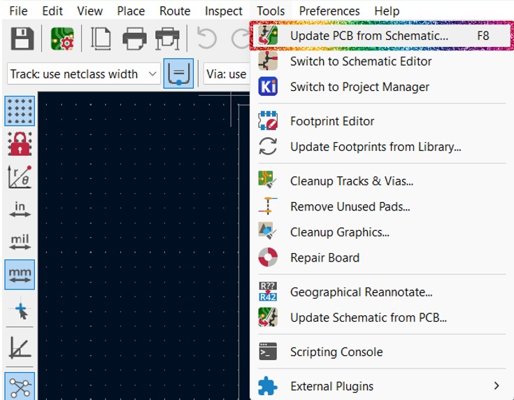
- Then click in the Update PCB button. In that way all the components will be imported into the workspace to be
freely moved wherever needed.
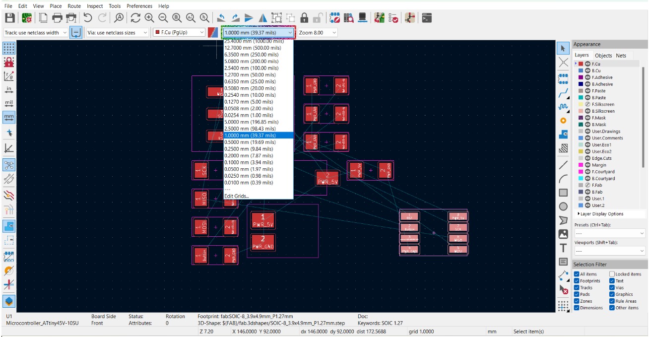
- To change the grid size I clicked in the next tab:
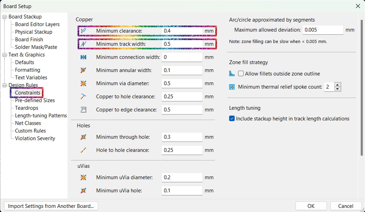
- Also I had establish the design rules for the traces. For this I clicked in File and then Board Setup....
- The design rules that I changed are Minimum clearance and Minimum track width, which are found in the
Constraints section.
- To create the paths between the components, I clicked the x key while the cursor is over the part to be joined. When
the key is clicked and the part to be connected is selected, the other possible connections to that part will be illuminated
as shown in the image below:
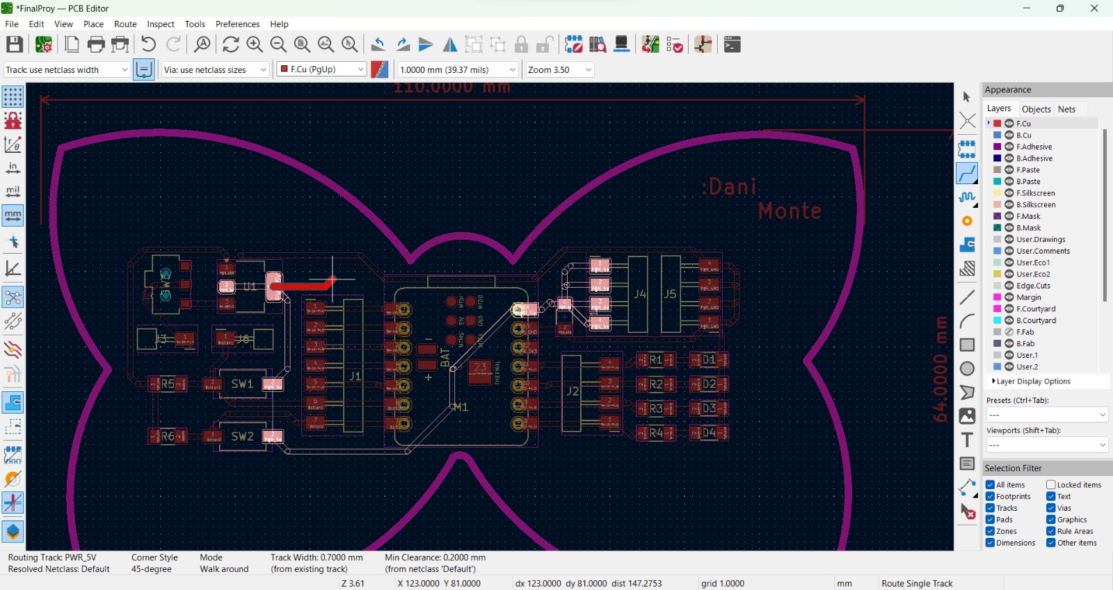
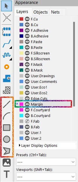
- I also selected the Margin layer and drew a shape for the margin using the drawing tools located in the right bar.
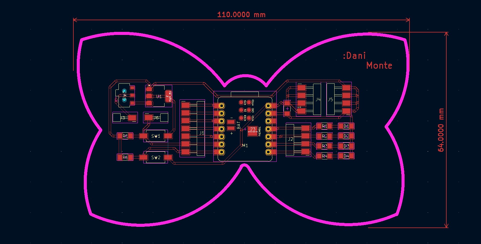
- Once I made all the paths and finished the margin it looked like this:
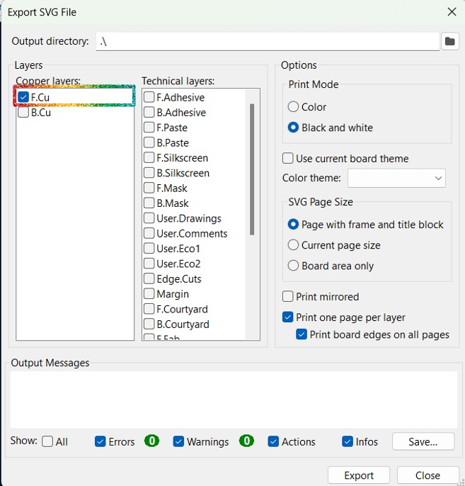
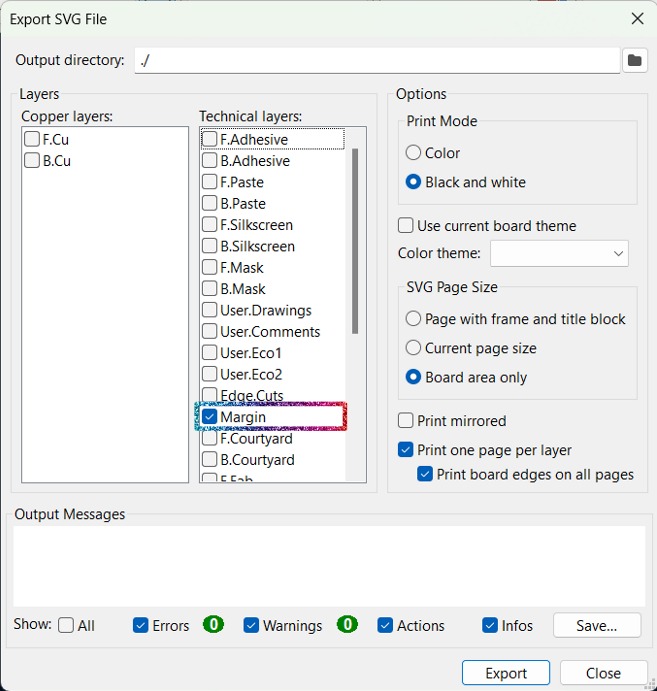
- Finally, I exported the outline and the toolpath by clicking in File, then Export, and SVG...
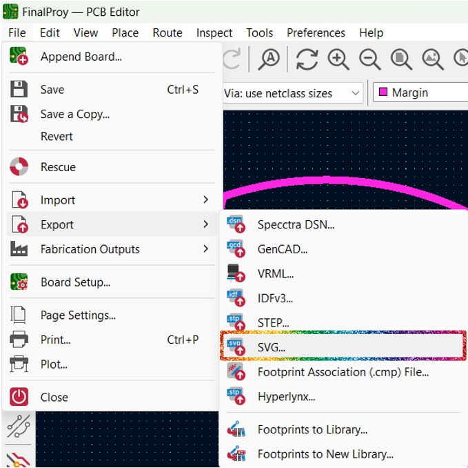
- I exported the F.Cu layer and the Margin layer.
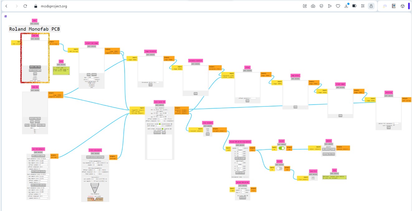
RML Files Creation
In order to cut in the Roland SMR-20 machine I needed the RML files. For this I followed the same steps as in week 4 when using the Mods Project page. However, this time I used the option to use the SVG files (on week 4 i had a PNG file).
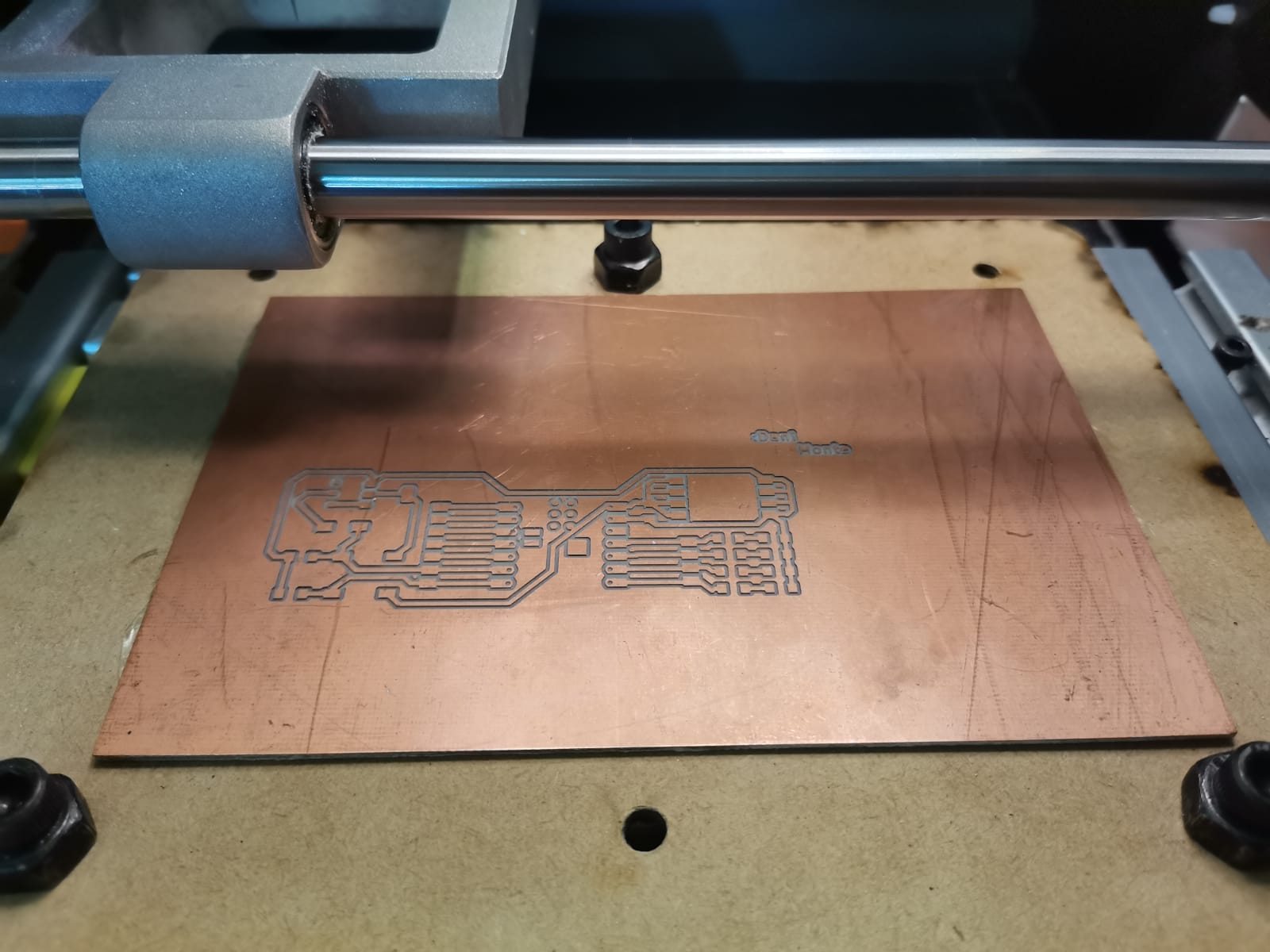
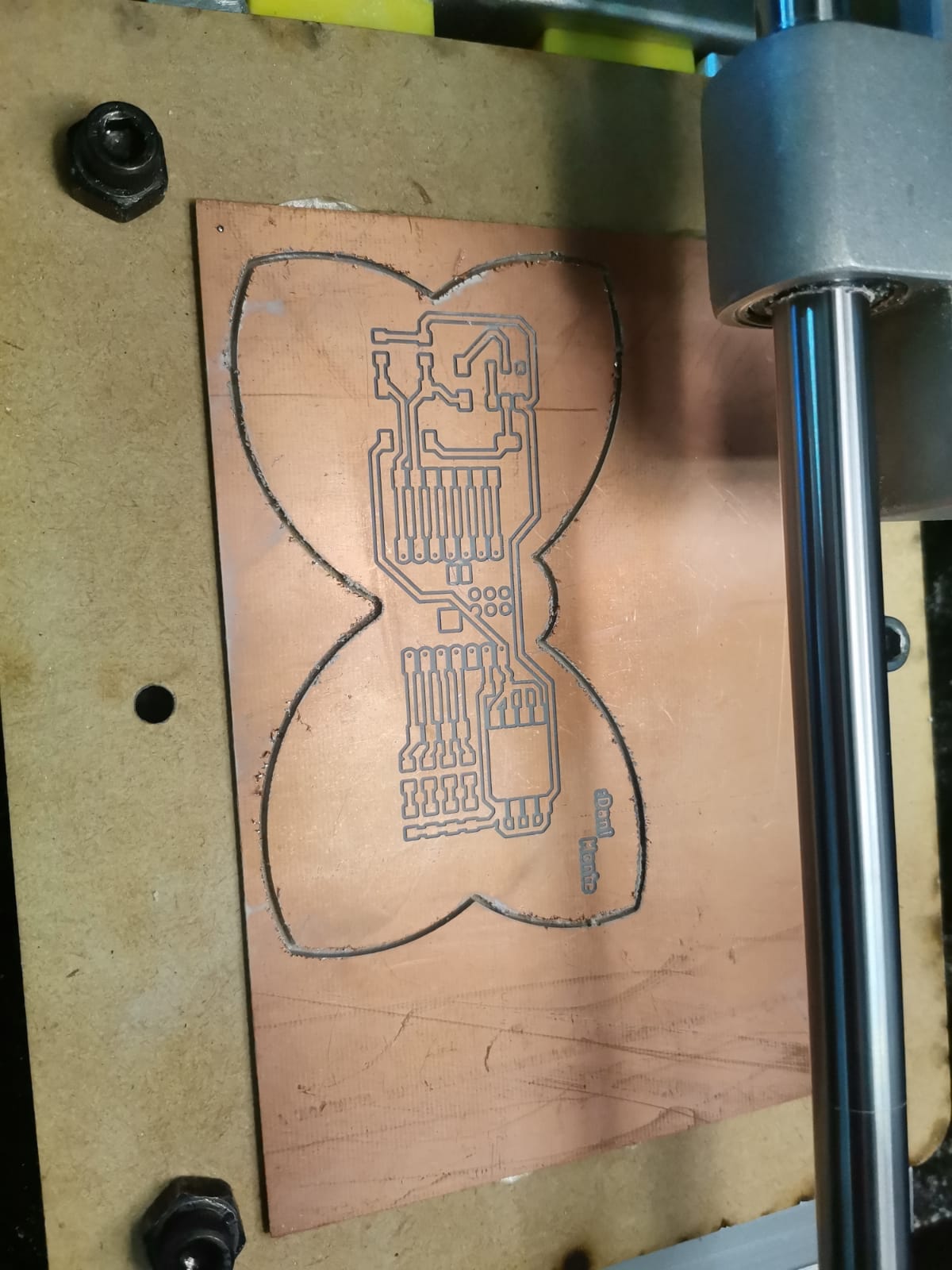
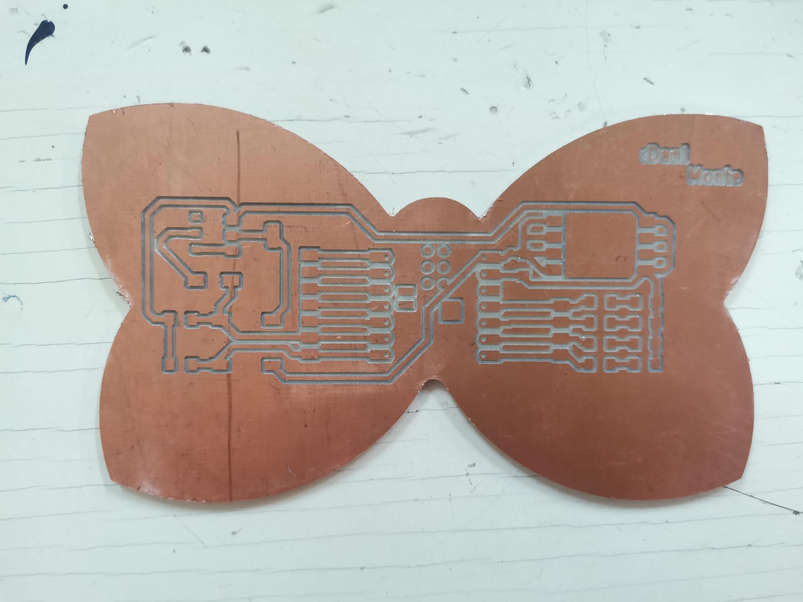
Cutting and Soldering of the PCB
For the cutting I used the Roland SMR-20 machine as in week 4 and followed the same steps to cut it. First, I cut the traces of the circuit, then the outline and finally I wwas able to take it out of the working bed.
Finally, I only had to solder all the components to the PCB using the squematic (first picture) and the PCB (second picture). Then I had all the components in the correct place.
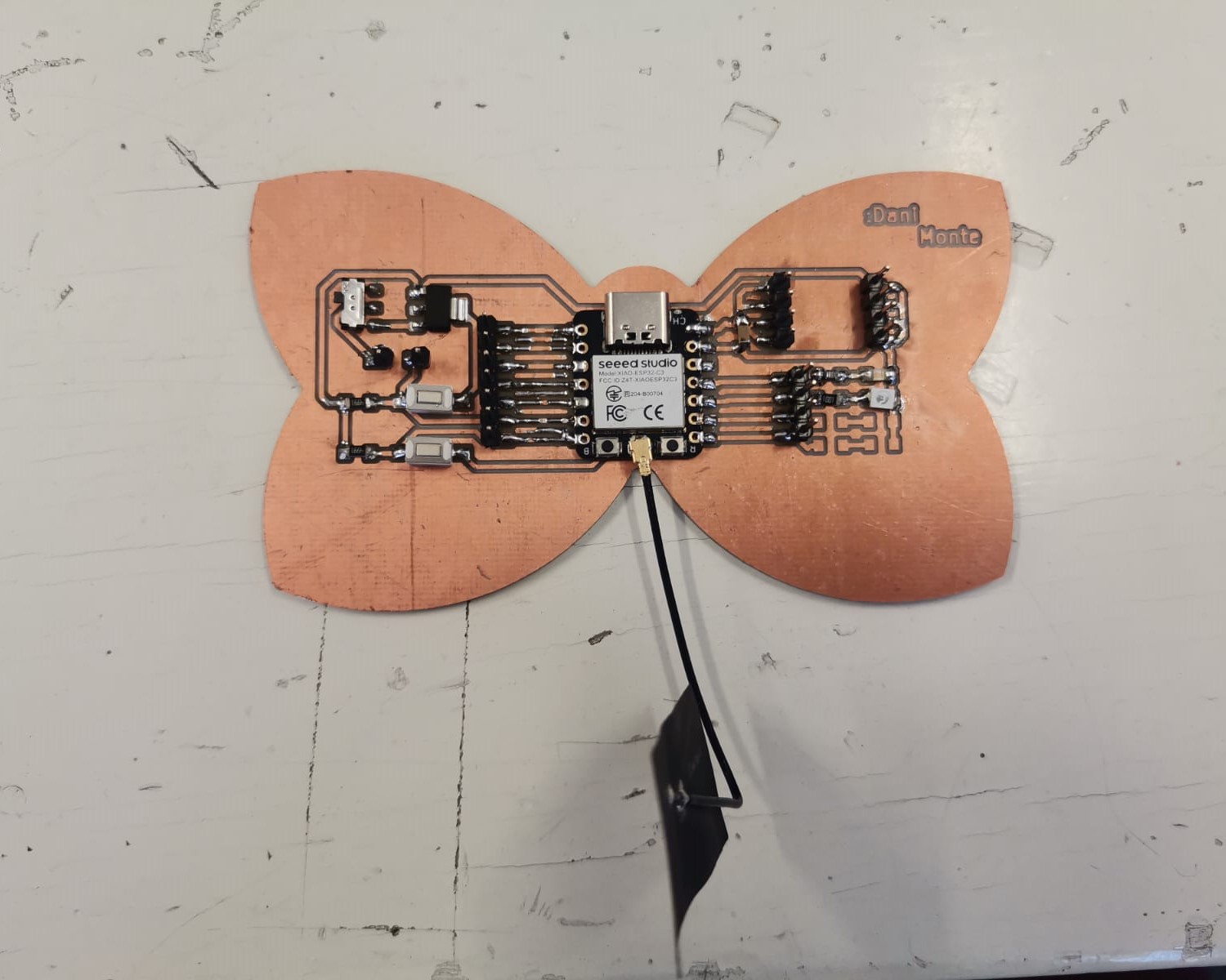
In the middle pictue it is possible to see that the GND path going to the J5 component touches the MTCK. However, this wasn't a big problem since I put insulation tape at the back of the Xiao to prevent any shortcircuit:
Trying Codes
I really didn't have something in mind, so I only tried programming what may be usefull for me. Here I included an interruption and the use of a button.
A button using while
This code has a main code that turns on the LEDs and in between there's a while, which makes the LEDs blink.
Interruption
I wanted to practice with an interruption so I did a code that has a LED blinking and the interruption comes when the button is pressed.
Problems
The main problem I had was that I wasn't able to upload the code into the microcontroller. What happened was that I assumed that the Xiao ESP32-C3 functioned just as the Xiao RP2040 (the one I used in week 4). However, this had a different way of working. Although the bootloader mode is accessed the same way as with the RP204, the way to upload codes to this one obeys to the next steps:
- Press the reset button.
- Press boot button while still pressing reset.
- Stop pressing reset button.
- Stop pressing boot button.
- Upload code.
- Press reset.
Then, once I had done that as the first time to change code, the next times I uploaded the code it updated automatically. But if I had any other problem uploading the code into the microcontroller, I'd follow those steps. However, I also solved the problem by only pressing the reset button when the code was already uploaded and didn't showed in the circuit.