8. electronics design
This was a very interesting week, I learned how to use a new software for designing PCB boards, which opened up a lot of possibilities for electronic designs. But, I won't lie, it was pretty tough given that everything was completely new. The hardest part was definitely the programming. I kept running into errors, and it didn't help that I had already soldered everything together. I had to make some cuts in the PCB just to get it programmed properly but in the end, I learned a lot!!
Beginners guide:
We had a class with Oliver Ochoa, one of our instructors where we learned how to use KiCad and the basics of designing PCB boards. In addition, we learned how to install a library that contains the necessary components tailored to our specific requirements and those available in the lab. Here are the basic steps to set up KiCad and begin designing boards.
First, download KiCad

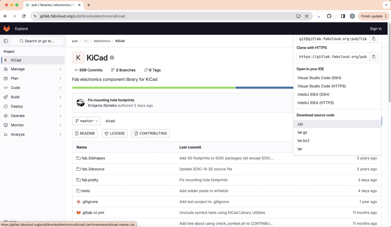
Then, to access specific libraries, download this zip file
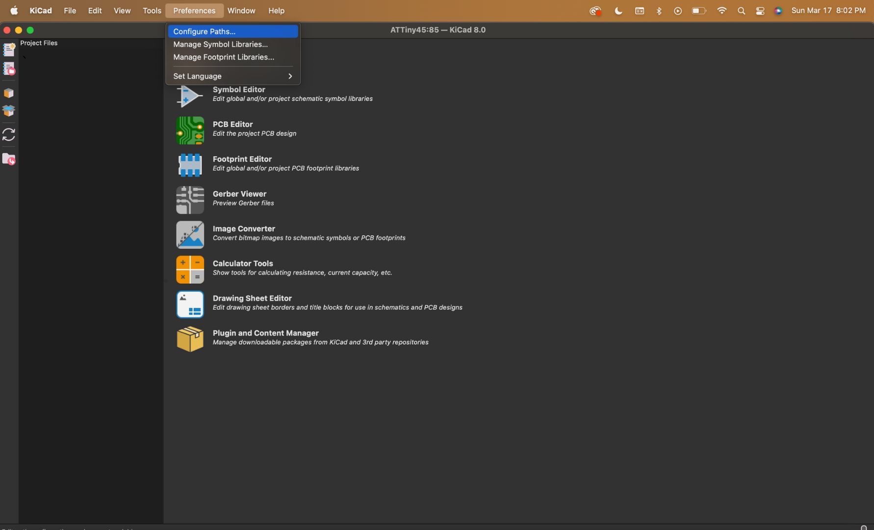
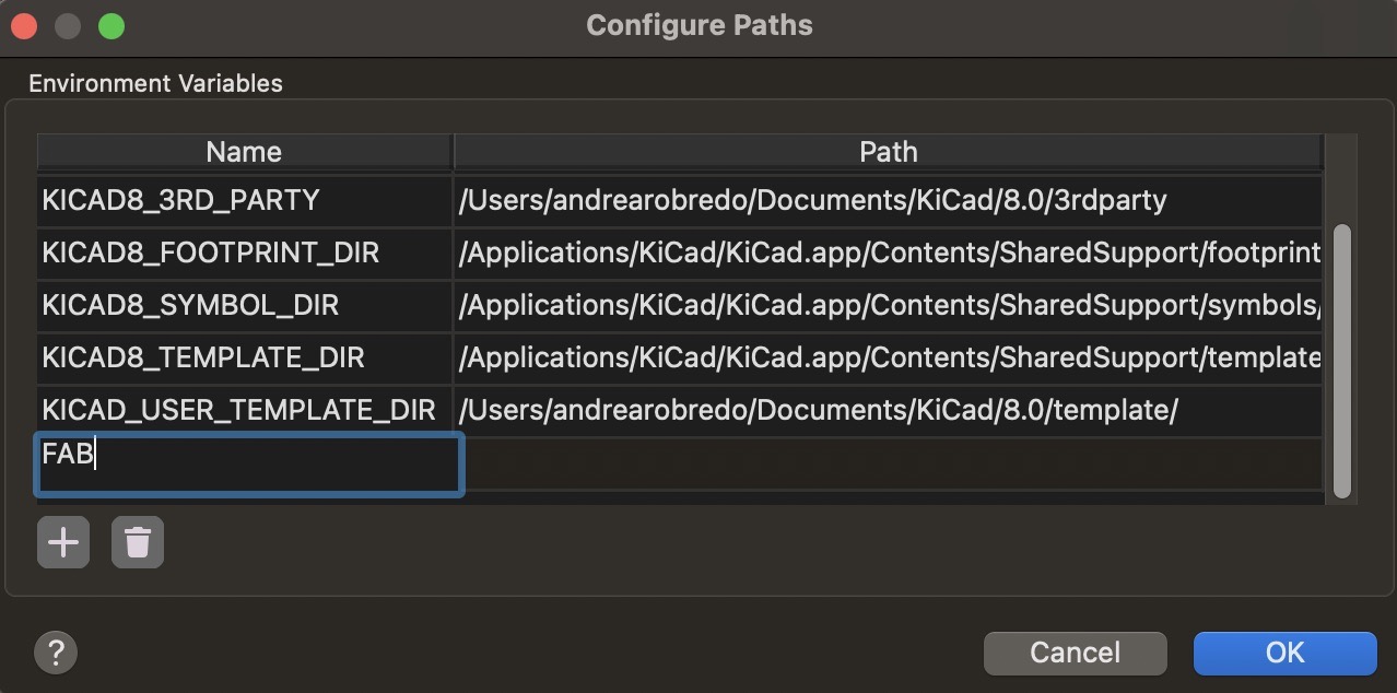
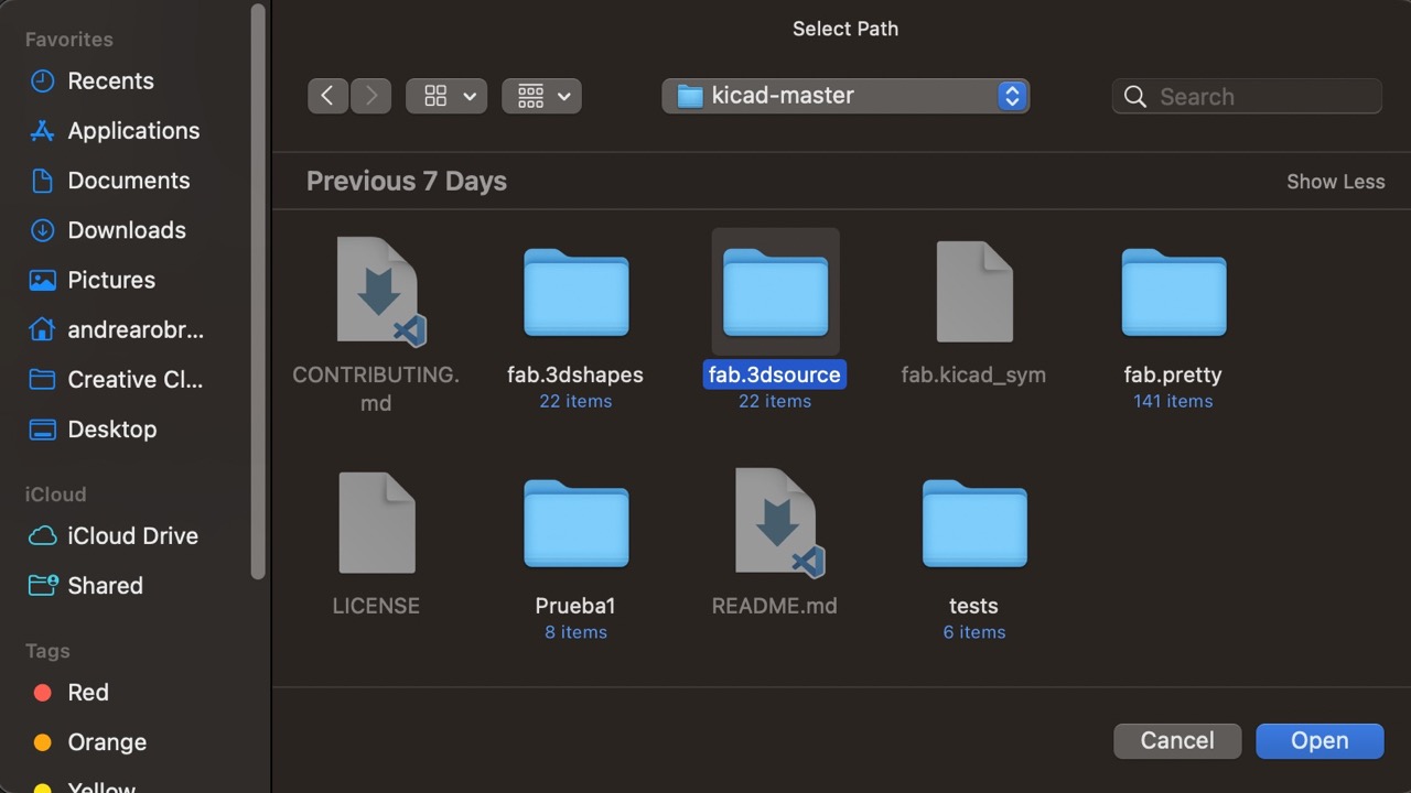
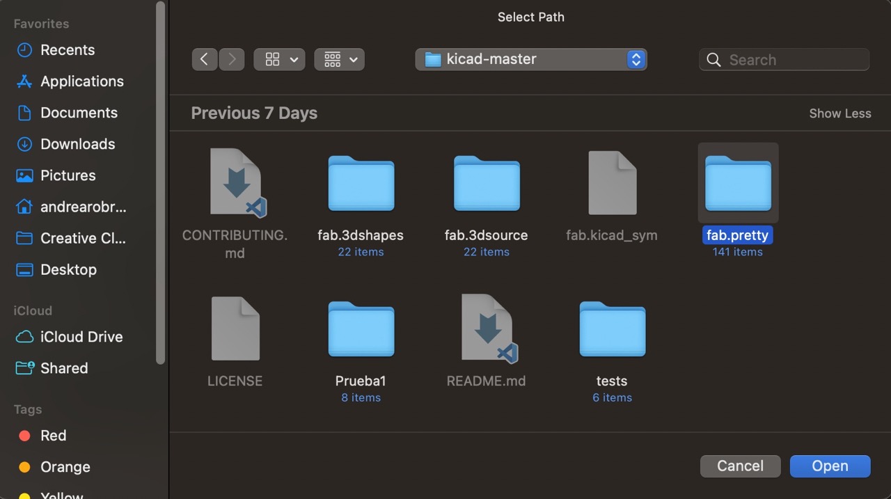
Now, let's integrate these libraries into KiCad. Open KiCad and navigate to the 'Preferences' menu, then click on 'Configure Paths'. Add a new path labeled 'FAB' and insert the 'fab.3dsource' folder.
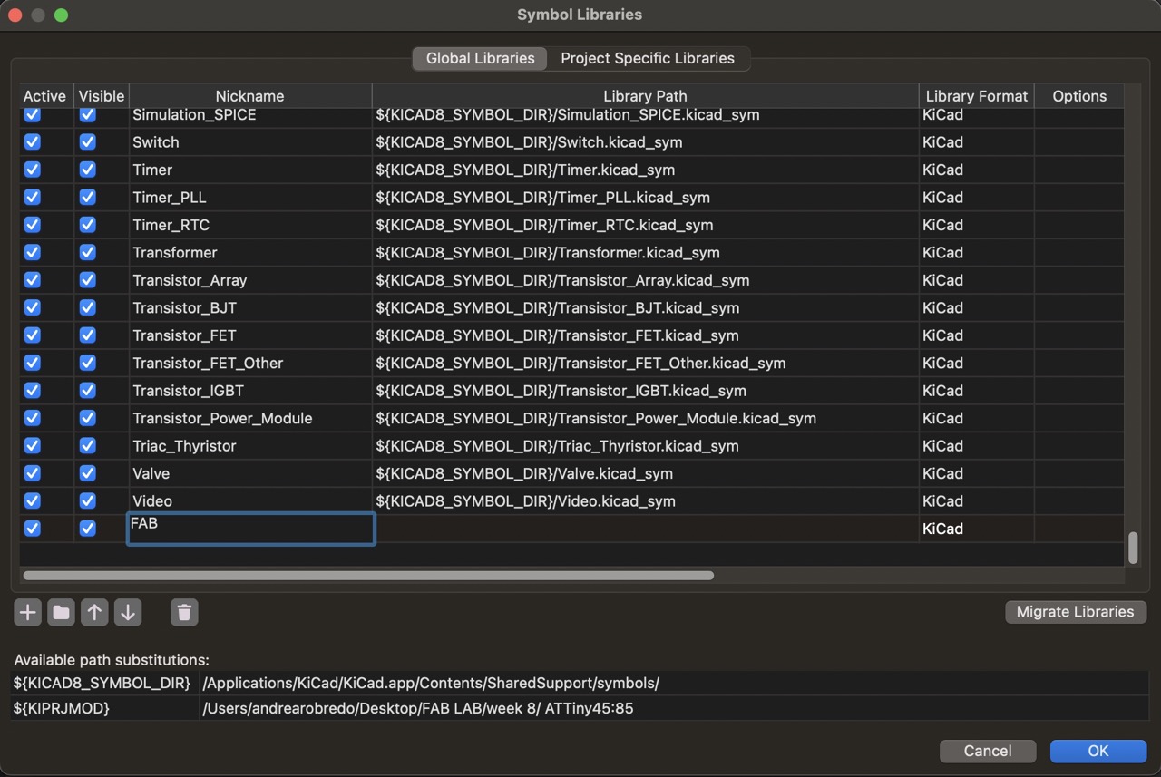
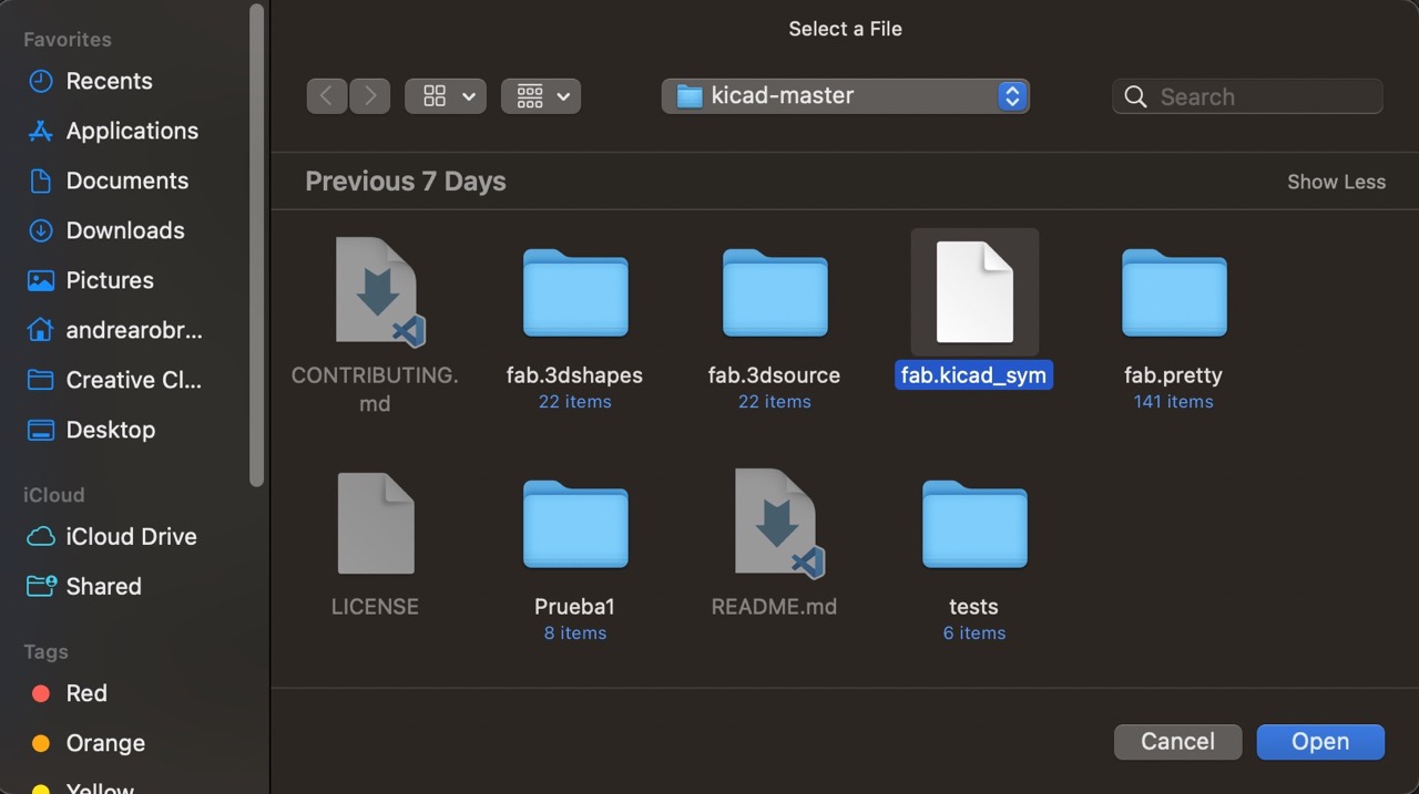
Proceed to 'Manage Symbol Libraries'. Once again, create a new 'Library Path' called 'FAB' and insert the 'fab.kicad_sym' file.

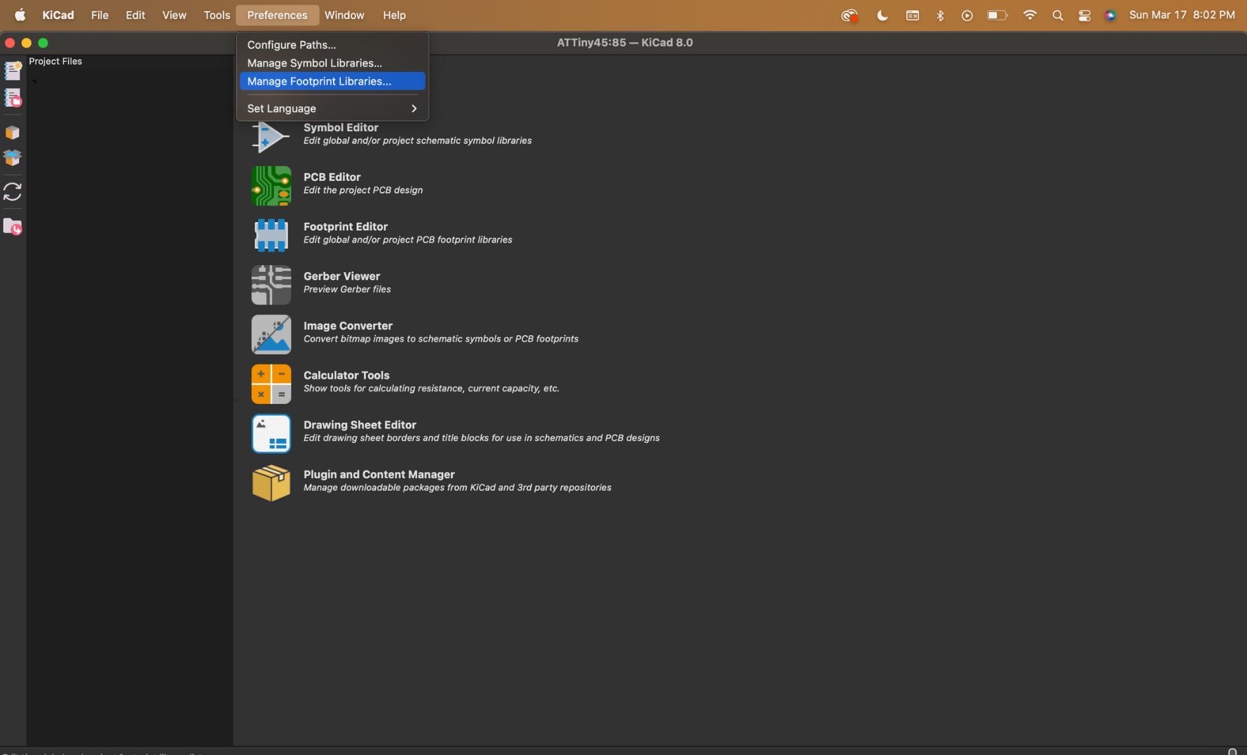
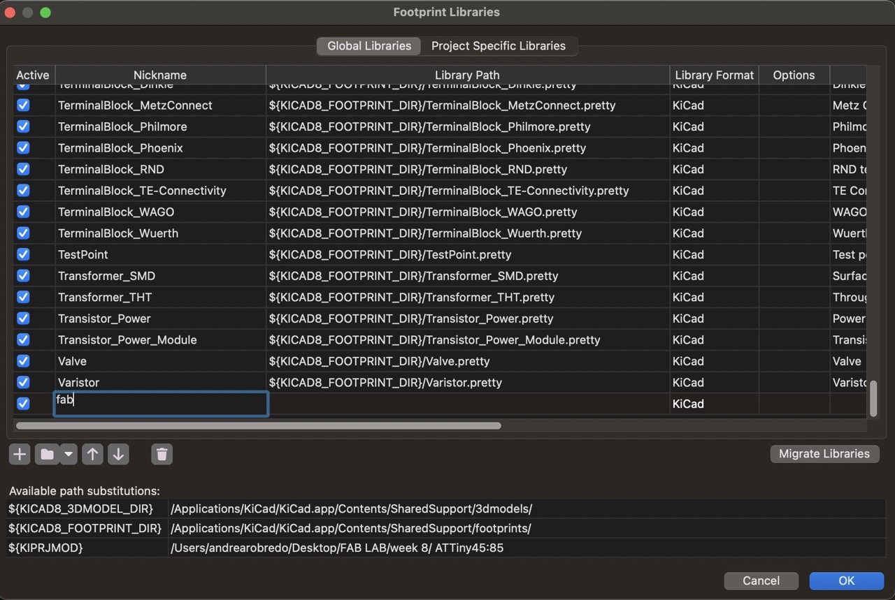
Finally, in 'Manage Footprint Libraries', establish a new path titled 'fab' and include the 'fab.pretty' folder.
Board Design
Design Idea
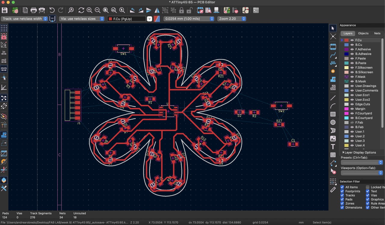
I was drawn to the idea of creating a LED flower. I believe there is something interesting in taking inspiration of the natural wonders and reimagining it as an electronic project.
Schematic Editor
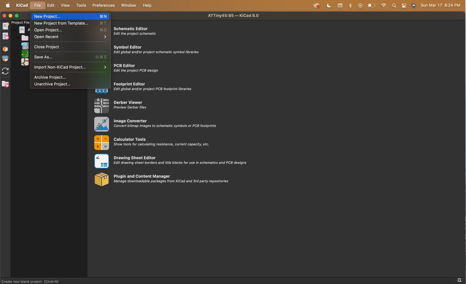
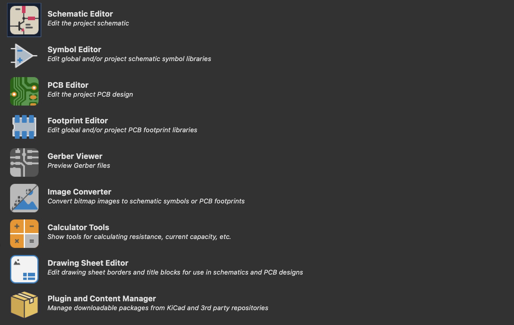
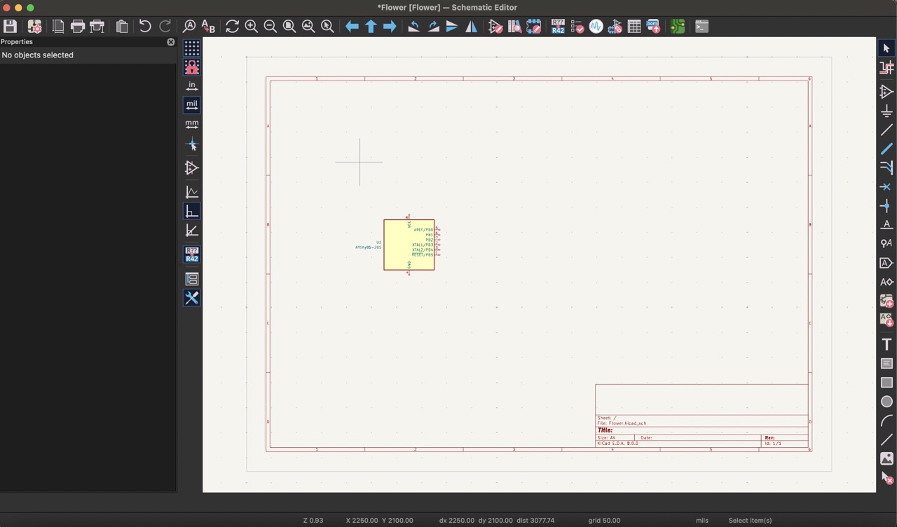
To begin, let's start a new project, click on the 'File' drop-down menu and select 'New Project'. Then, click on the ‘Schematic Editor’
In the following tables I will show you the basic tools and components needed to make the flower PCB design.
Basic tools used
Tool |
|
|---|---|
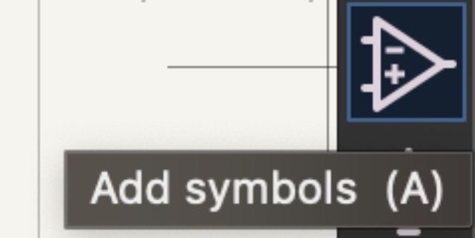
| Add symbols |
|
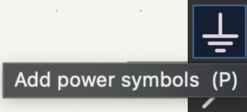
| Add power symbols |
|
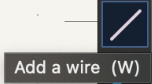
| Add a wire |
|
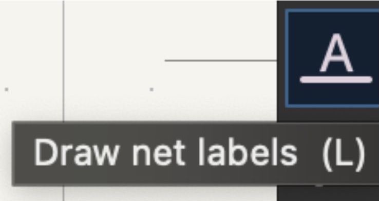
| Draw net labels |
|
Components needed
Physical components |
Quantity |
|
|---|---|---|
| ATtiny 85 | 1 |
|
| Button | 1 |
|
| Capacitor | 1 |
|
| Resistance | 27 |
|
| LED | 25 |
|
| Pins | 2 (3 pin bed) |
|
Power components |
|
|---|---|
| Ground |
|
| Volts |
|
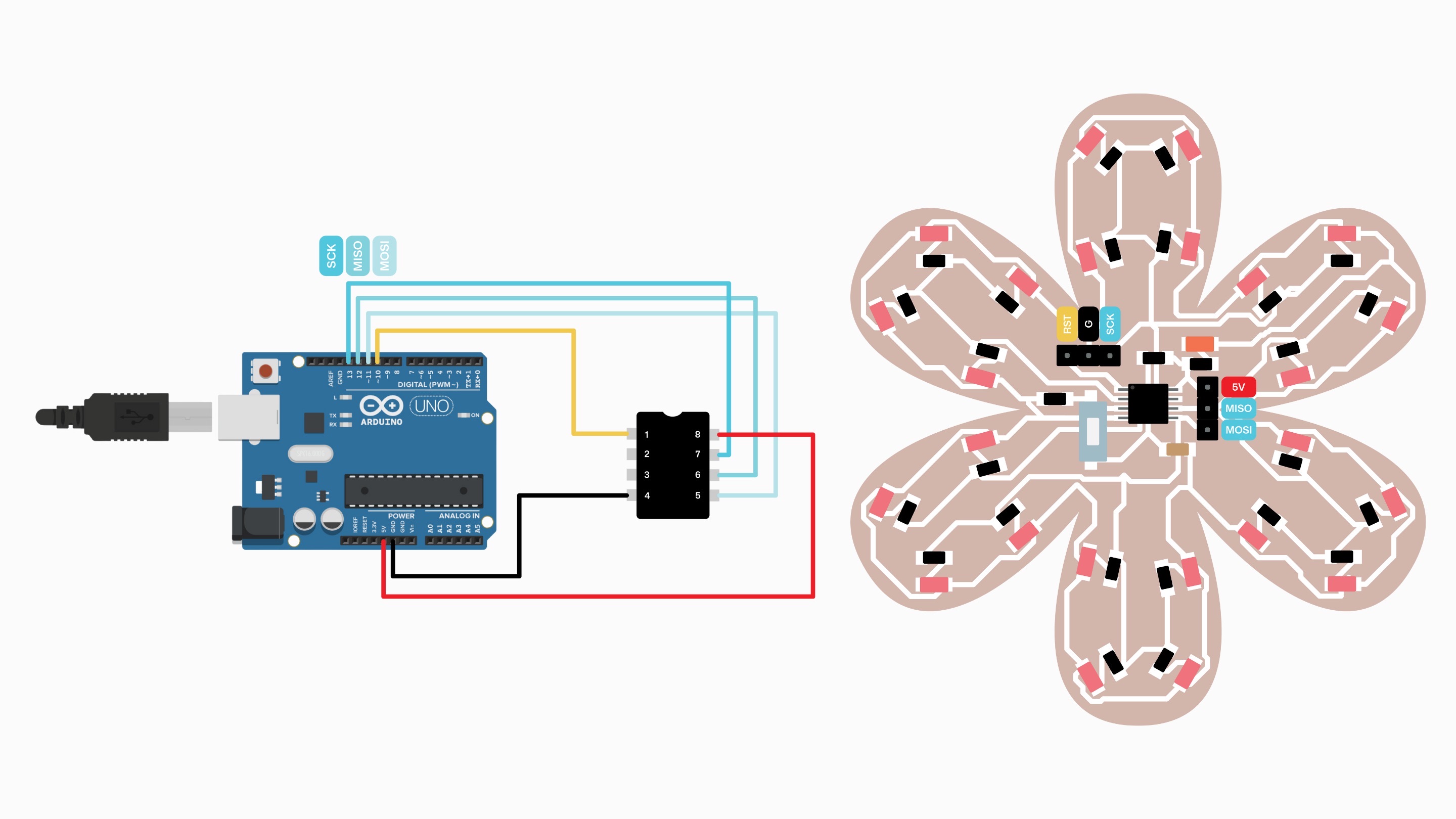
1:
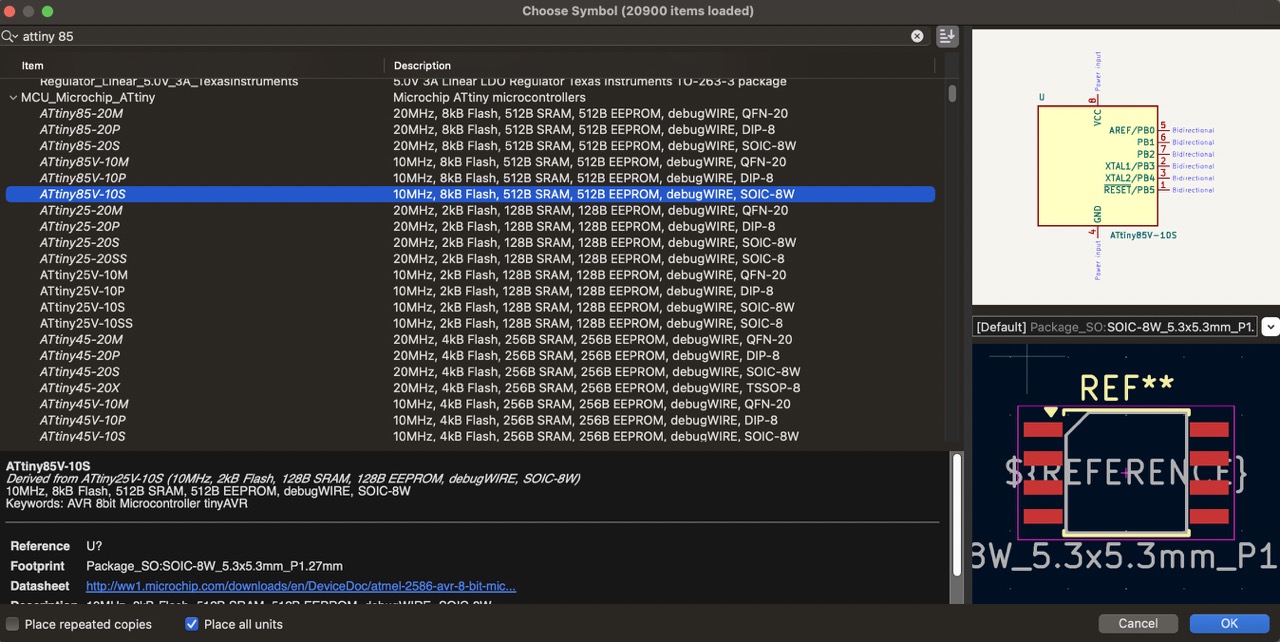
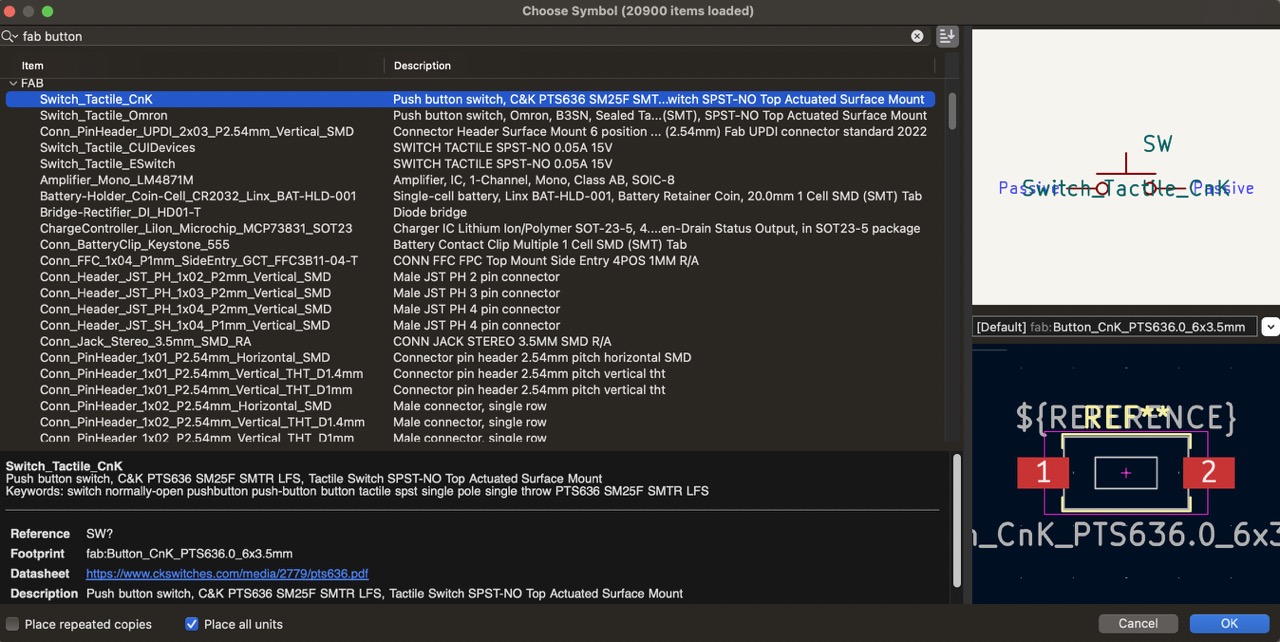
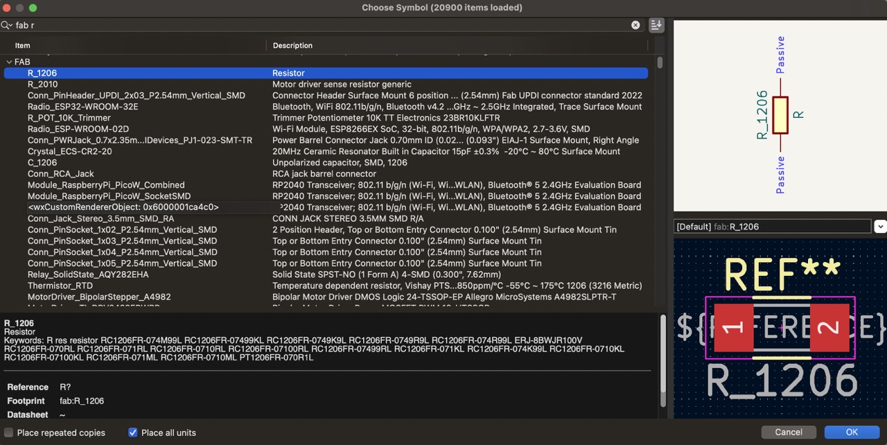
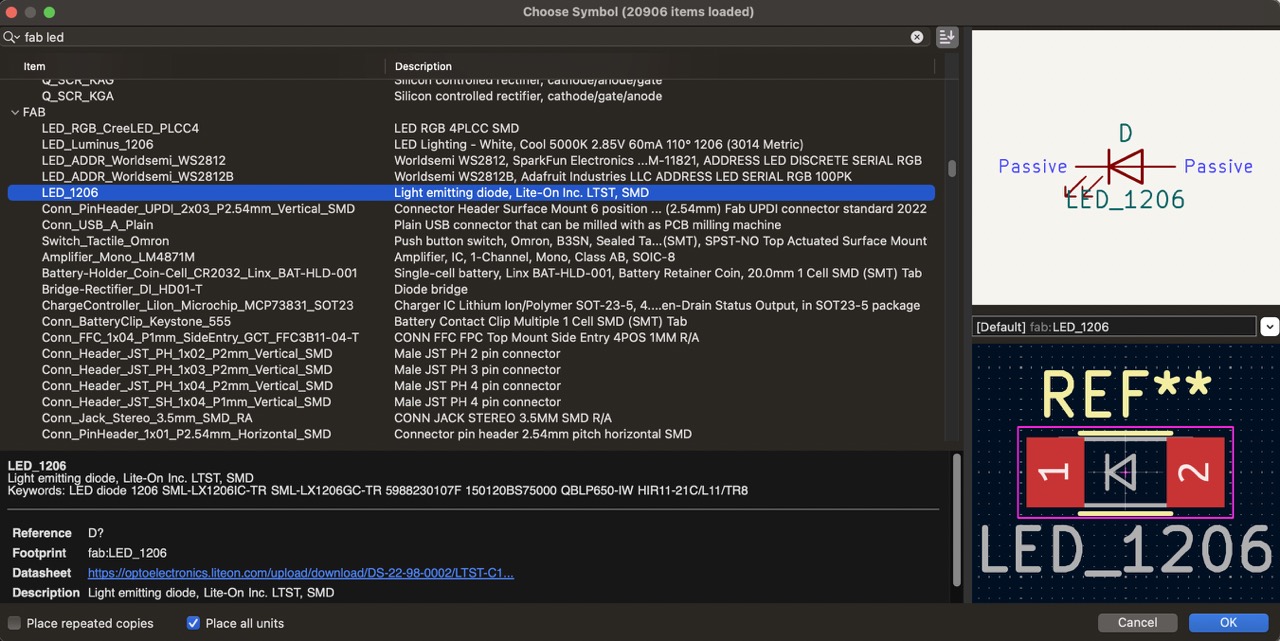
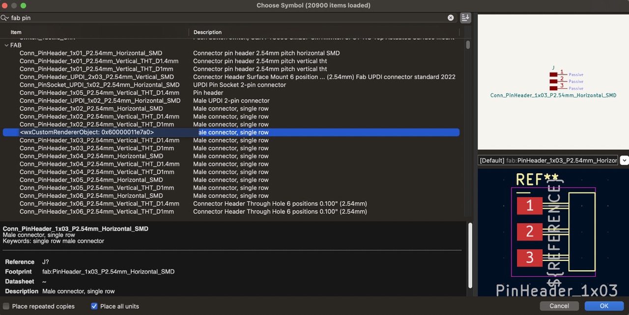
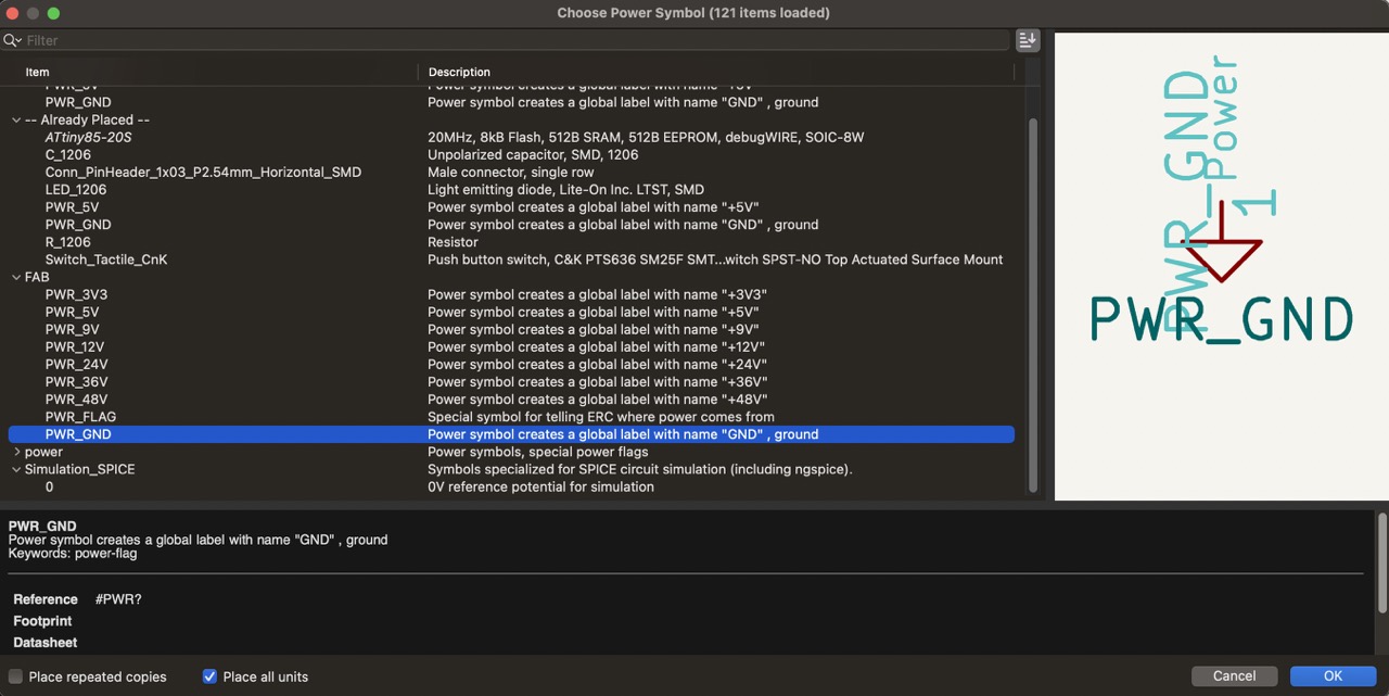
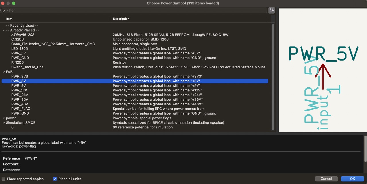
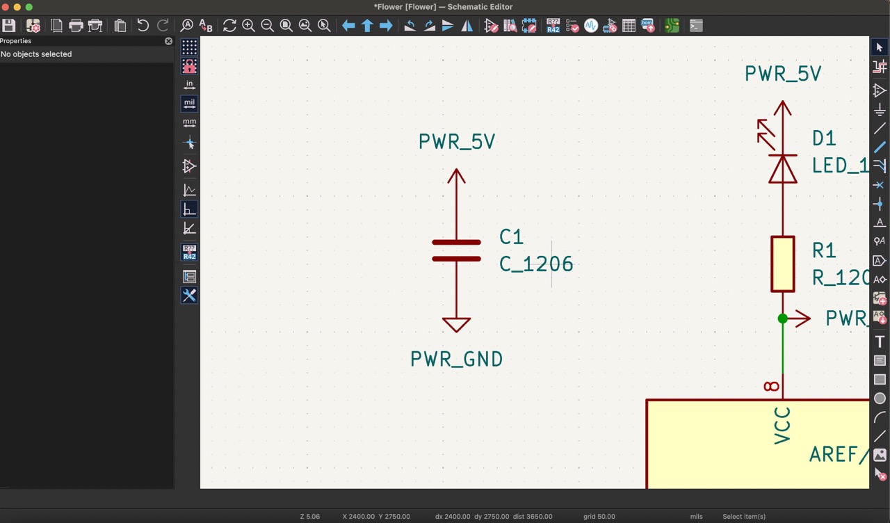
To begin, click on the ‘Add Symbol’ button and locate the Attiny85, select it and add it to the schematic. Next, connect the ground pin to the ground by clicking on the 'Add Power Symbol' and selecting 'PWR_GND'. Similarly, connect the VCC pin to 5V, followed by a resistor, an LED, and once again 5V. This LED will serve as a visual indicator to confirm power delivery to the ATtiny.


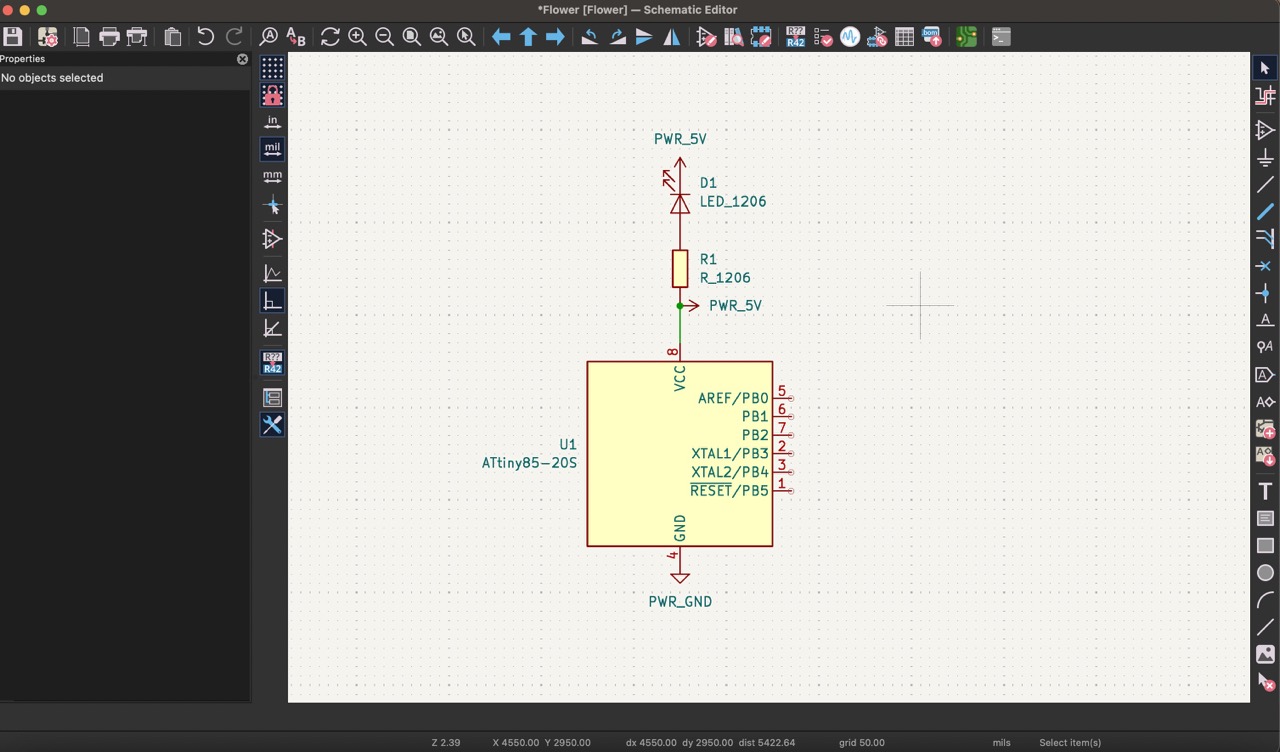
2:
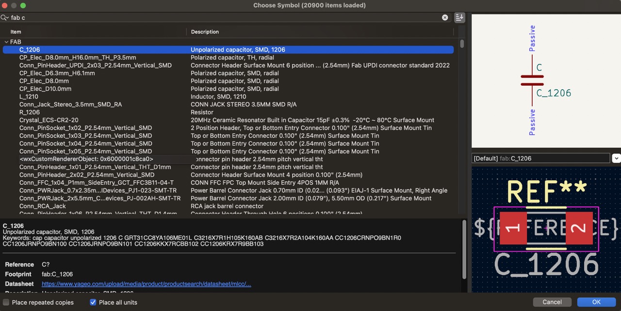
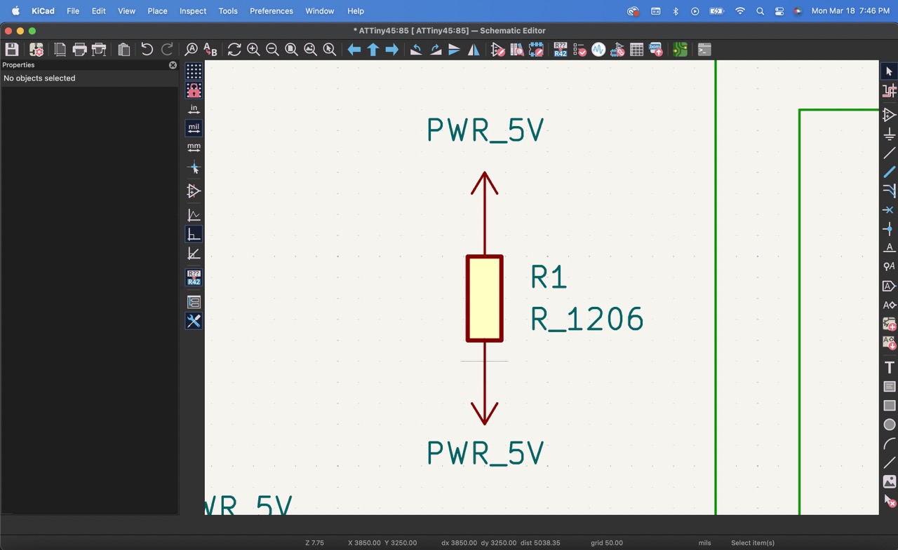
Now, incorporate a capacitor and connect it to both ground and 5V.

3:
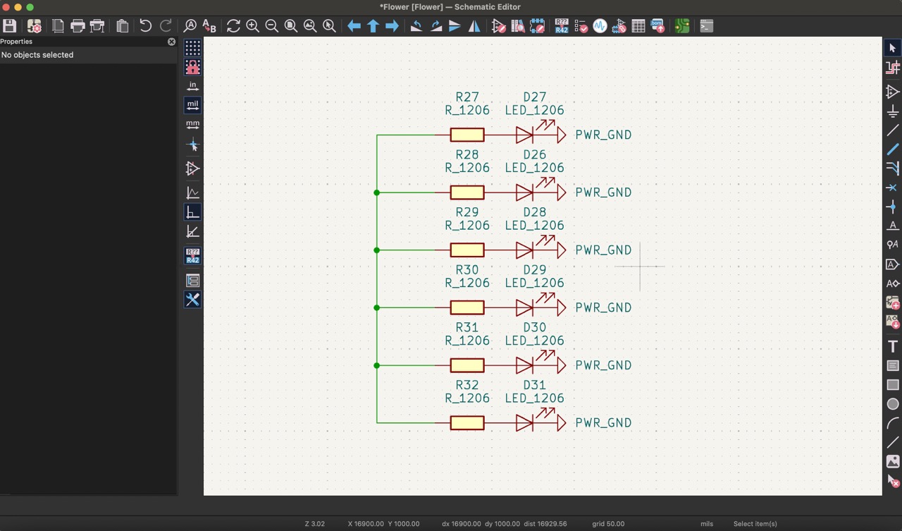
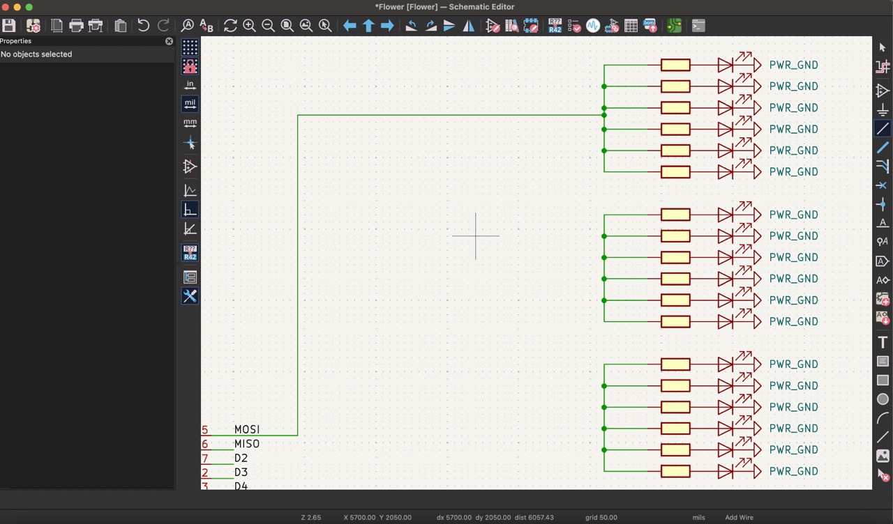
Moving on to the LEDs, each pin will accommodate six, begin by placing a resistor, followed by an LED, and connect them to ground.


4:
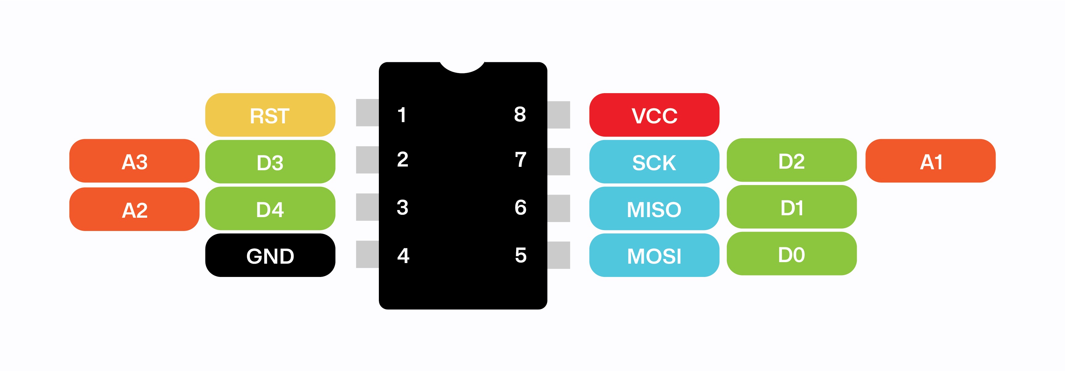
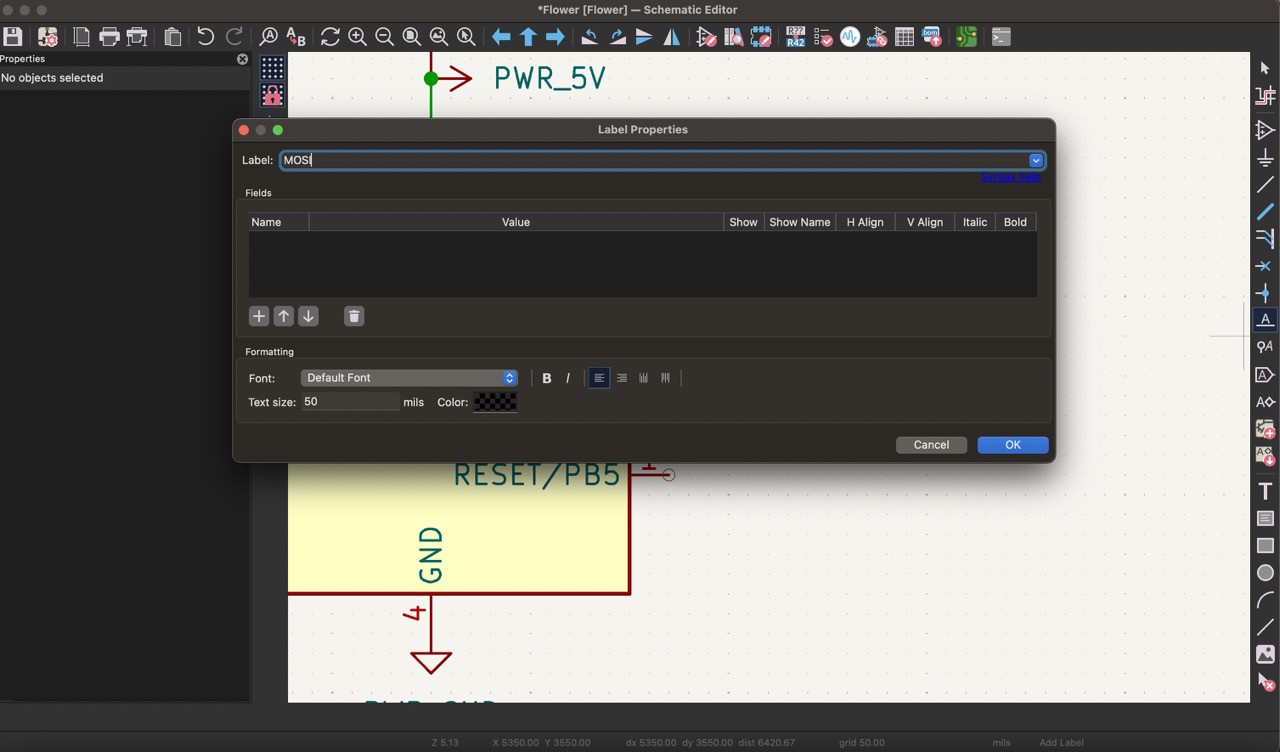
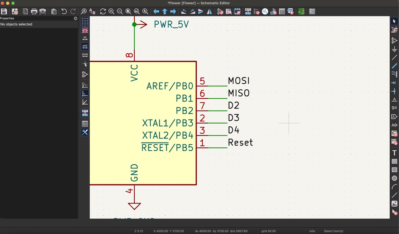
Using the 'Draw net labels' tool and referring to the Attiny 85 setup, label the pins to determine the appropriate connections for the LEDs. The selected pins are 5, 6, 7, and 2. Use the 'Add a wire' tool to link these pins to each LED group.


5:
Next, add a button to pin 3. Attach a resistor between the pin and the ground, and connect the button between the pin and 5V.

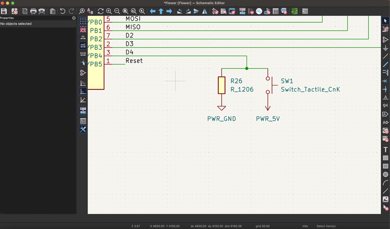
6:
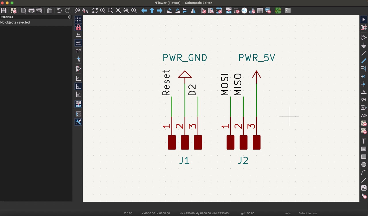
Finally, integrate two pin beds consisting of three pins each. Use the 'Draw net labels' tool to link them to the reset, ground, d2, mosi, miso, and 5V.

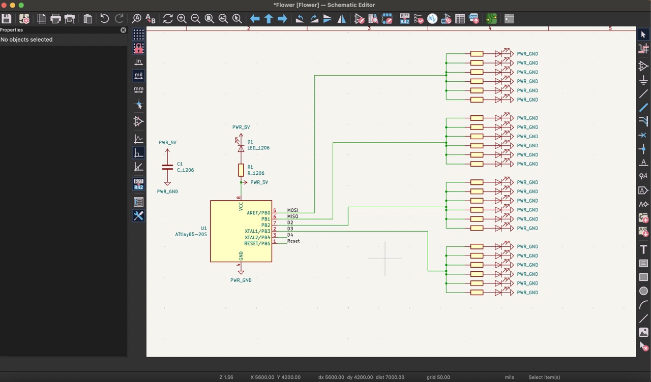
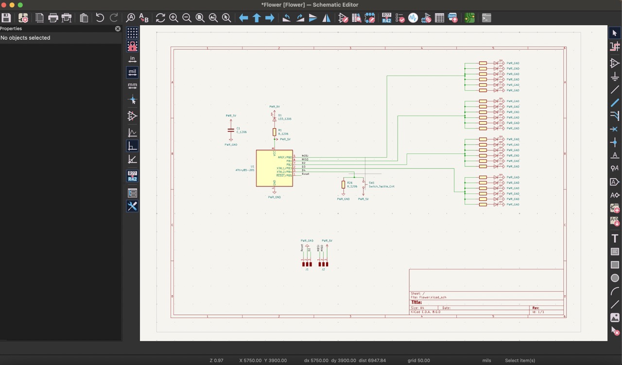
7:
This is what the final schematic looks like.
PCB Editor
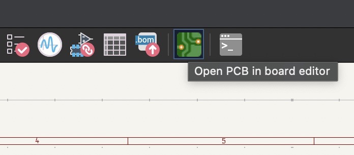
1:
Now, navigate to the top right corner menu and click on the green button labeled ‘Open PCB in board editor’.
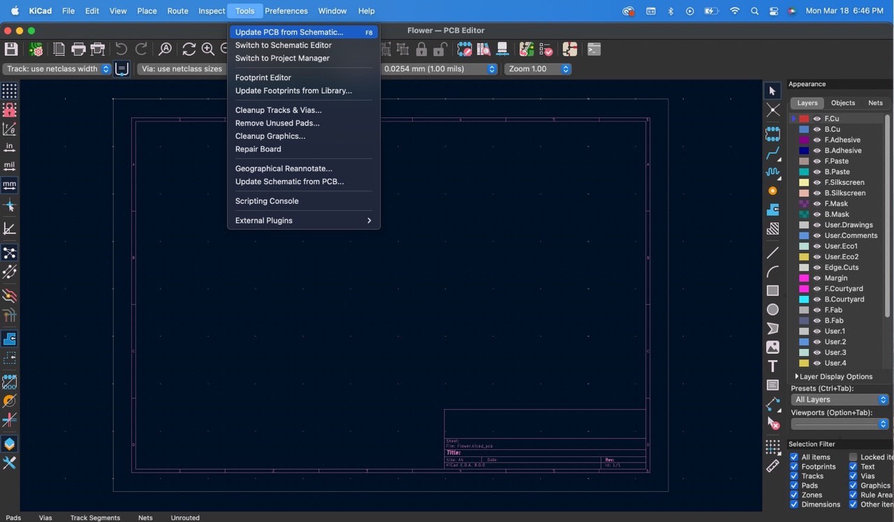
2:
From the 'Tools' drop-down menu, choose 'Update PCB from Schematic' to insert the components into the board layout.
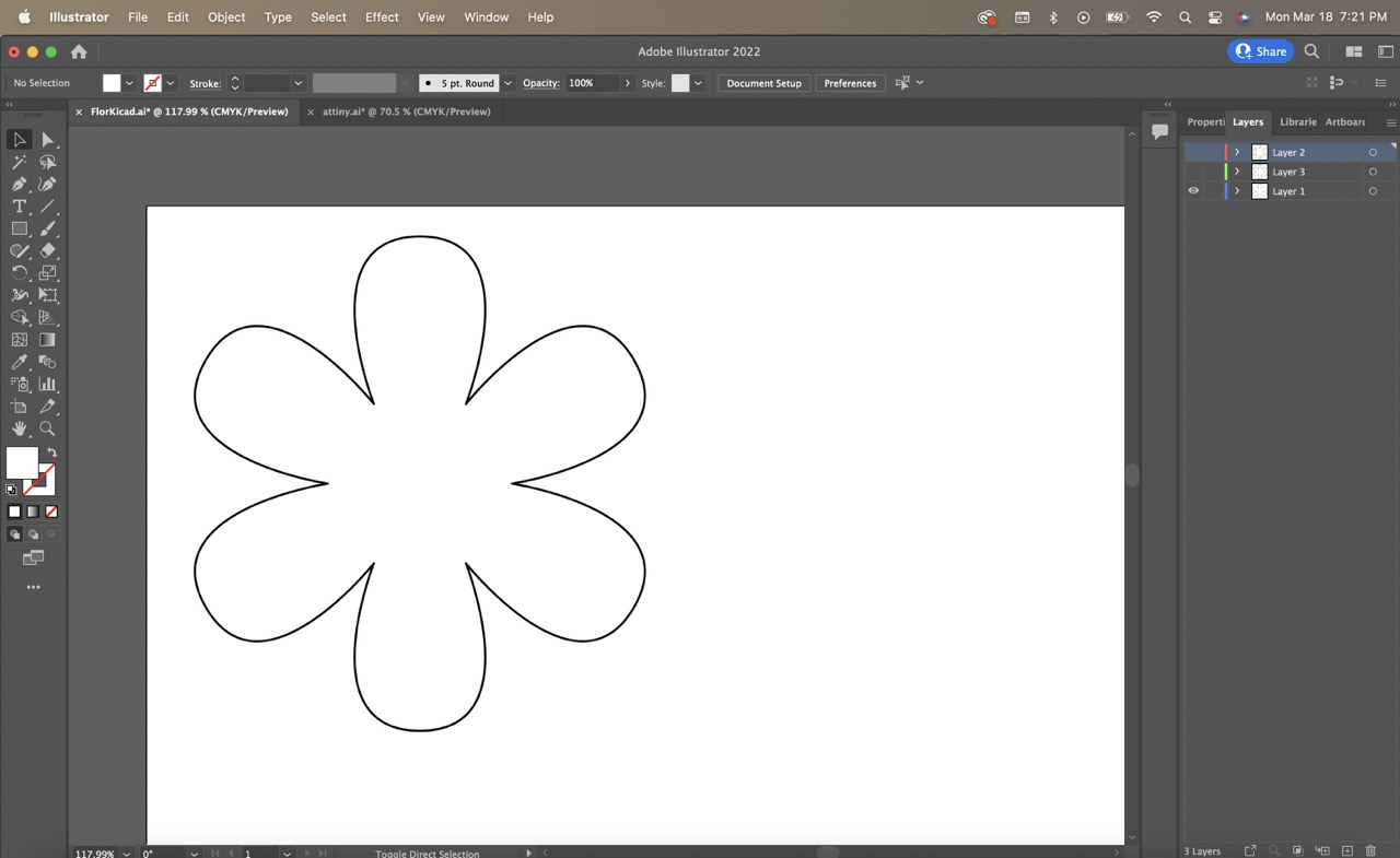
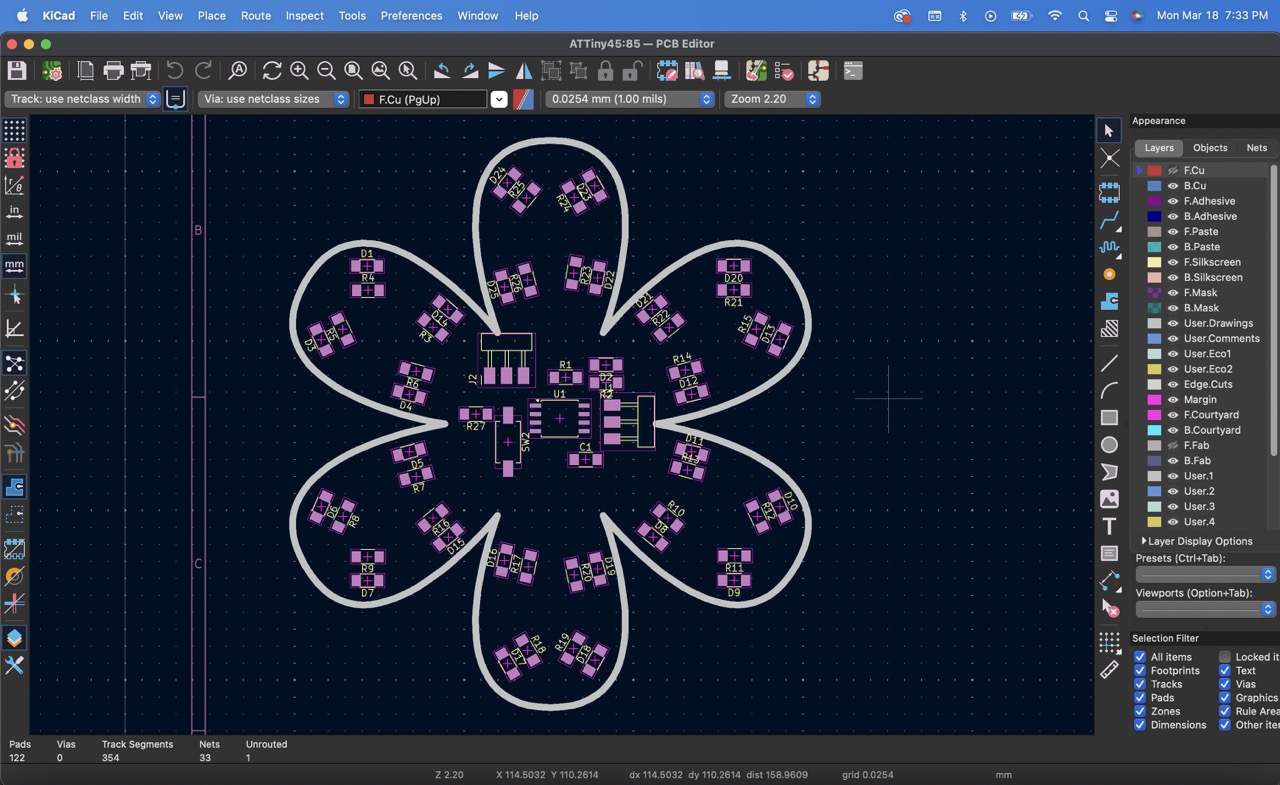
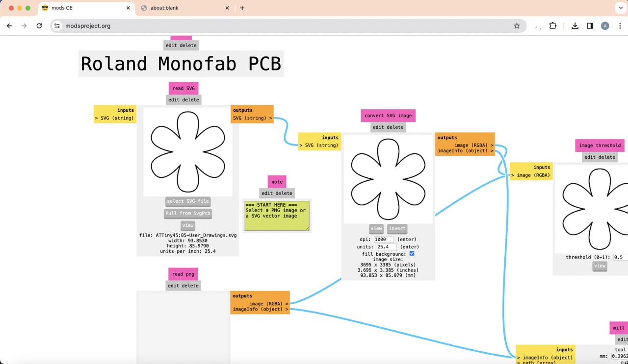
3:
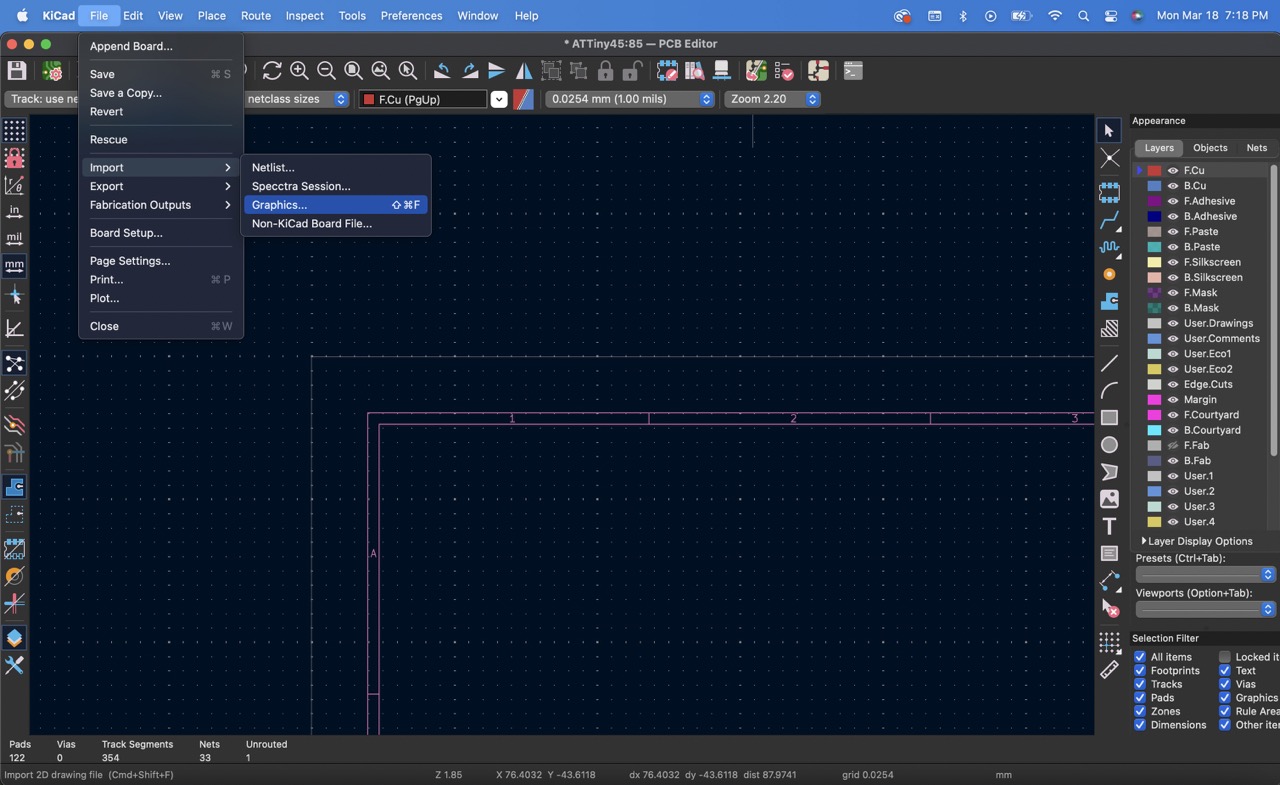
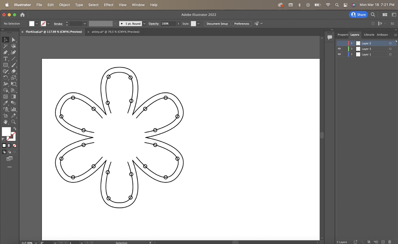
In Illustrator, I outlined the flower design and saved it as a .dxf file. Back in KiCad, I selected the ‘user drawing’ layer and imported the flower file by accessing the 'File' drop-down menu, clicking on ‘Import’, and selecting ‘Graphics’.
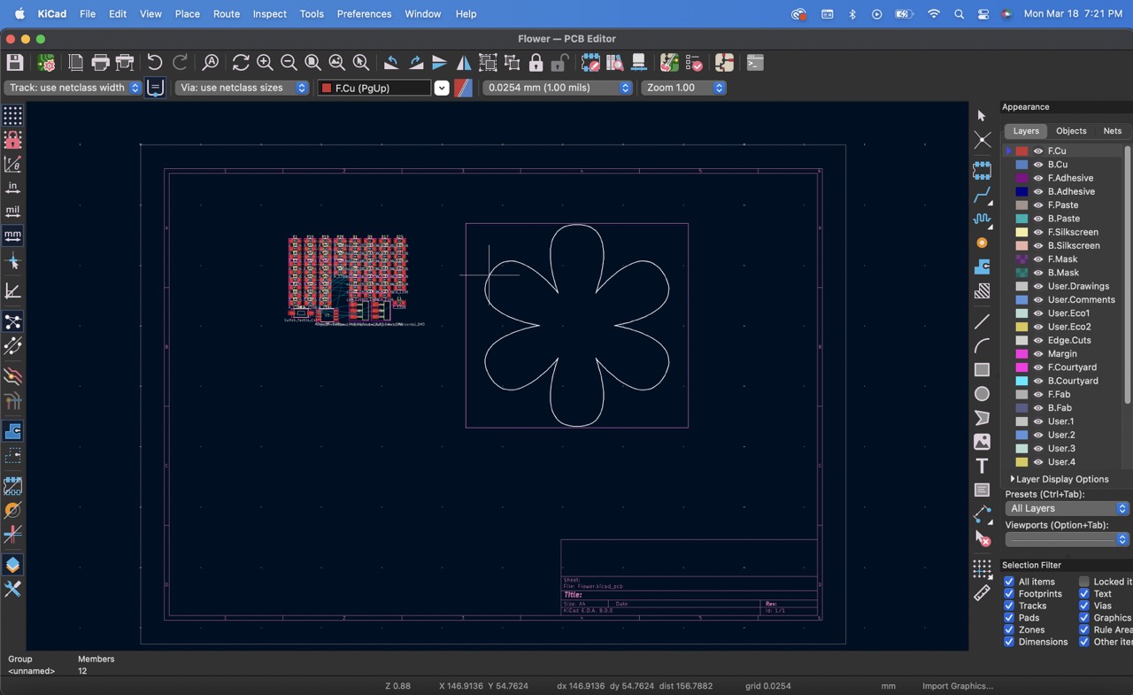
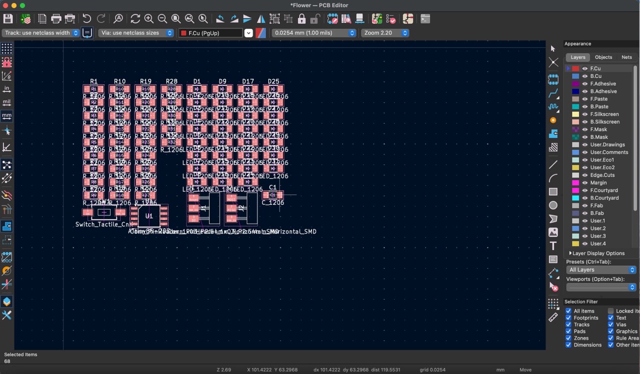
4:
I then proceeded to arrange each component within the flower, ensuring they were positioned adjacent to their corresponding connections to facilitate track placement. During this process, I realized that for a better result, I needed to rotate the LEDs and resistors to align with the petals angles.
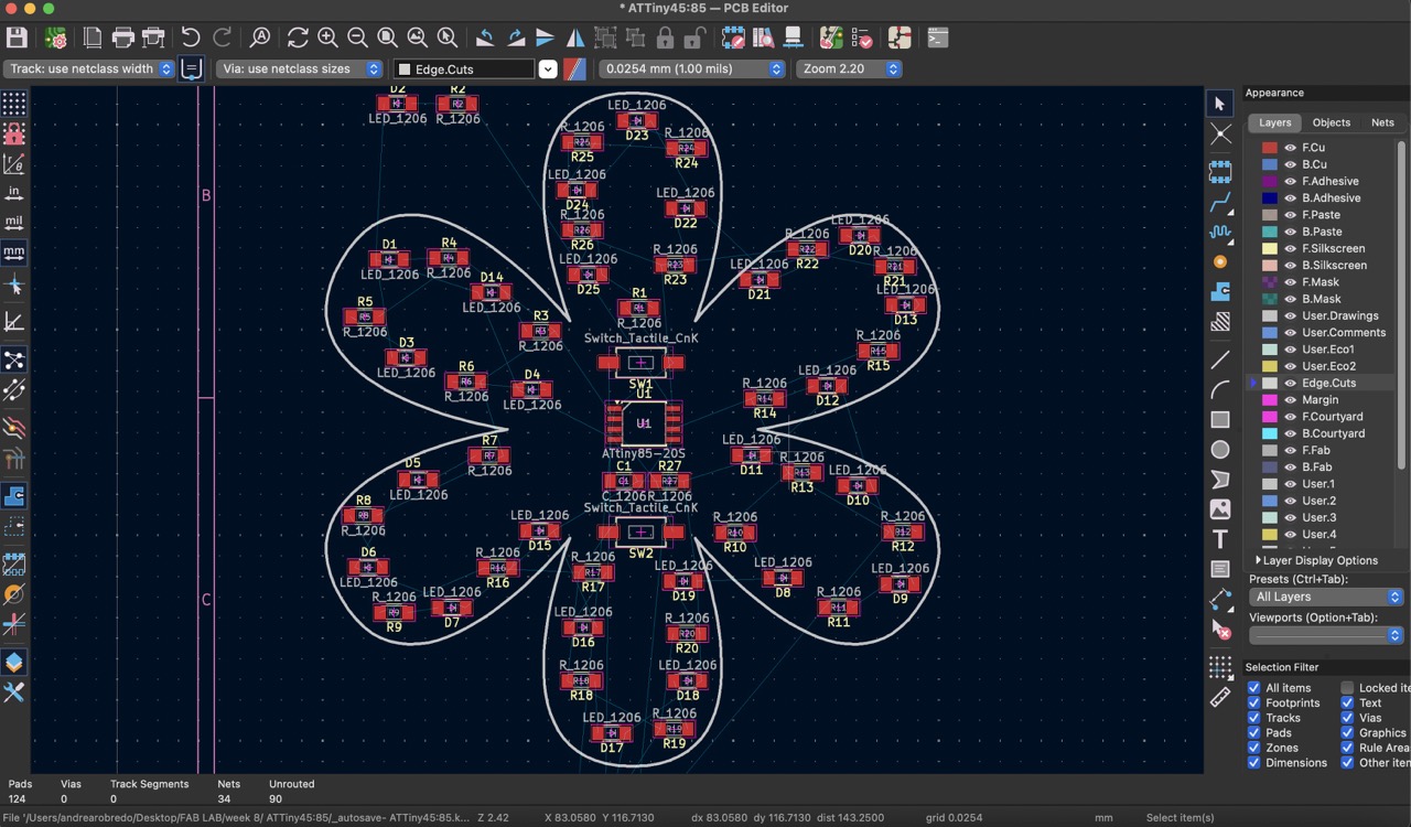
5:
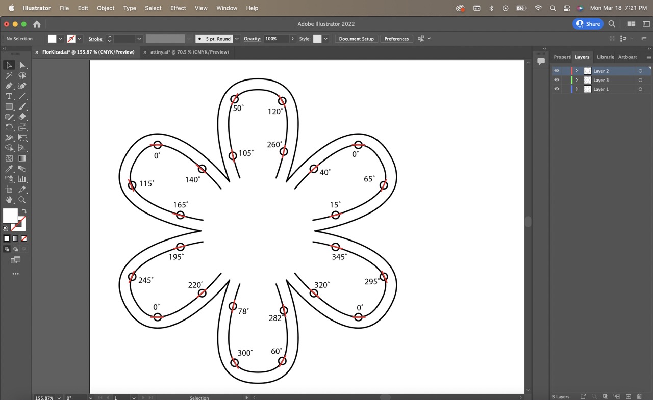
To achieve this, I went back to Illustrator and offseted the trace towards the inside and added four circles on each petal to determine the angles, saved the file as a .dxf once more, and imported it into KiCad. Using the PCB Editor, I double-clicked on each resistor and LED to rotate them according to the angles determined in Illustrator.
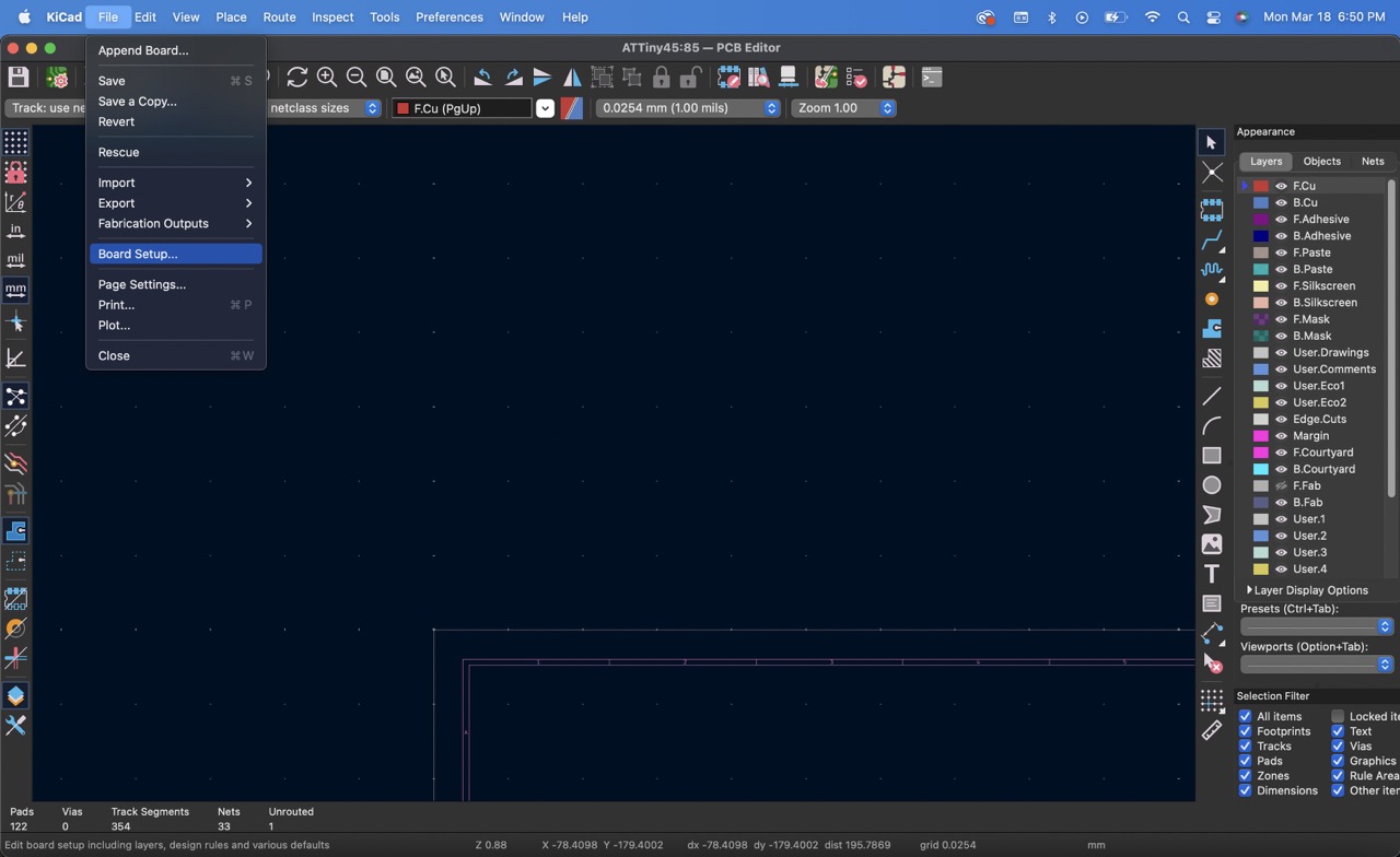
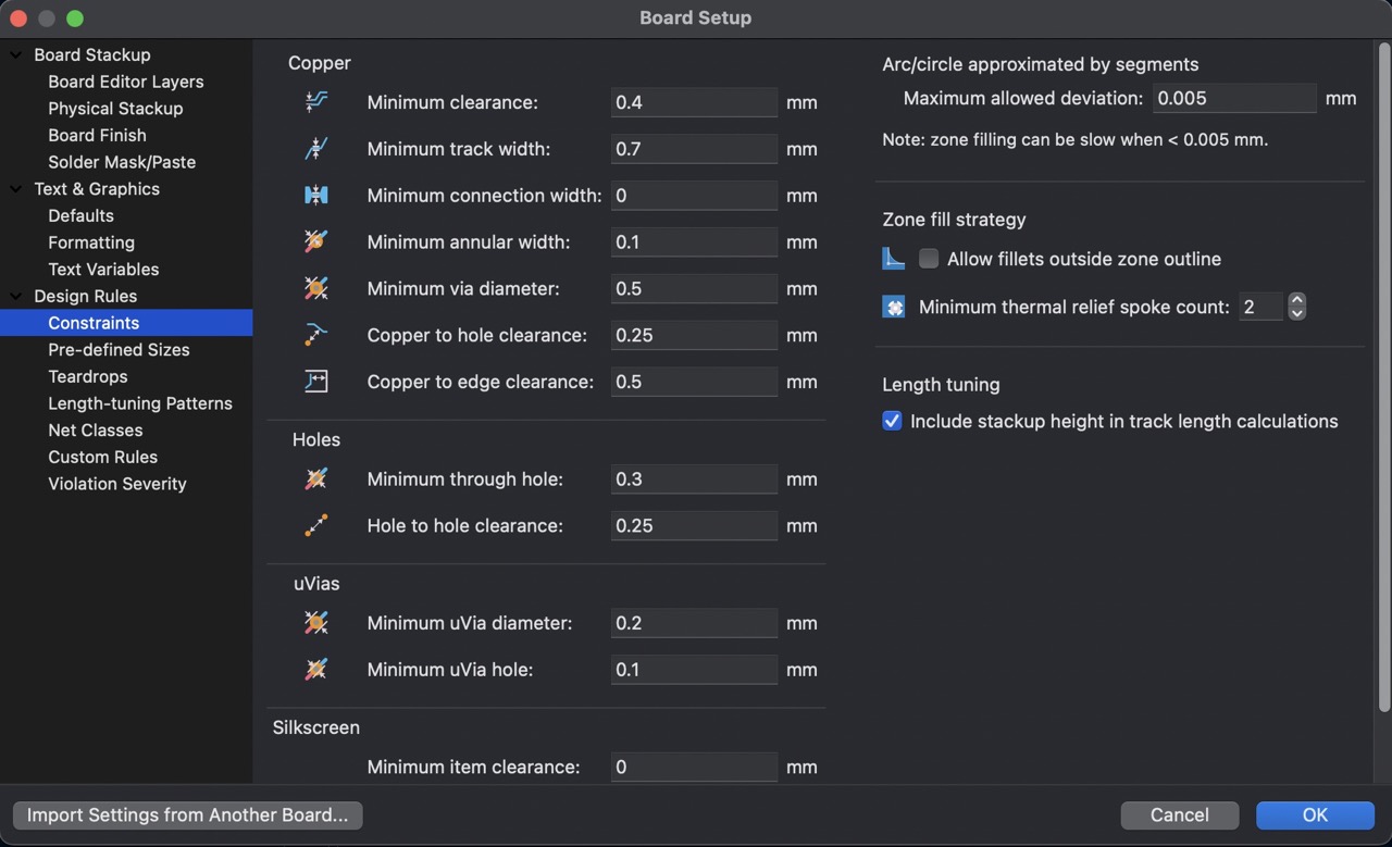
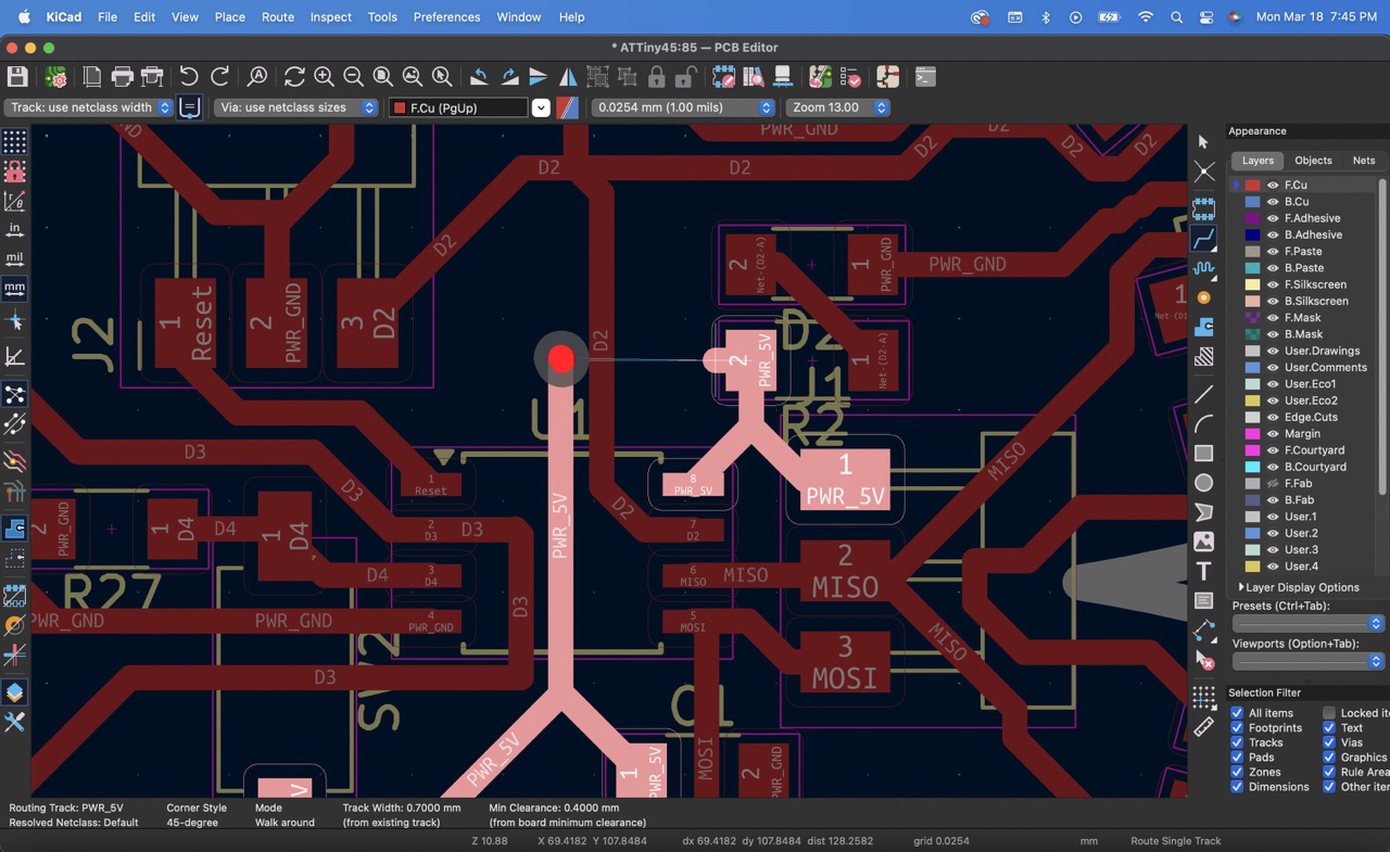
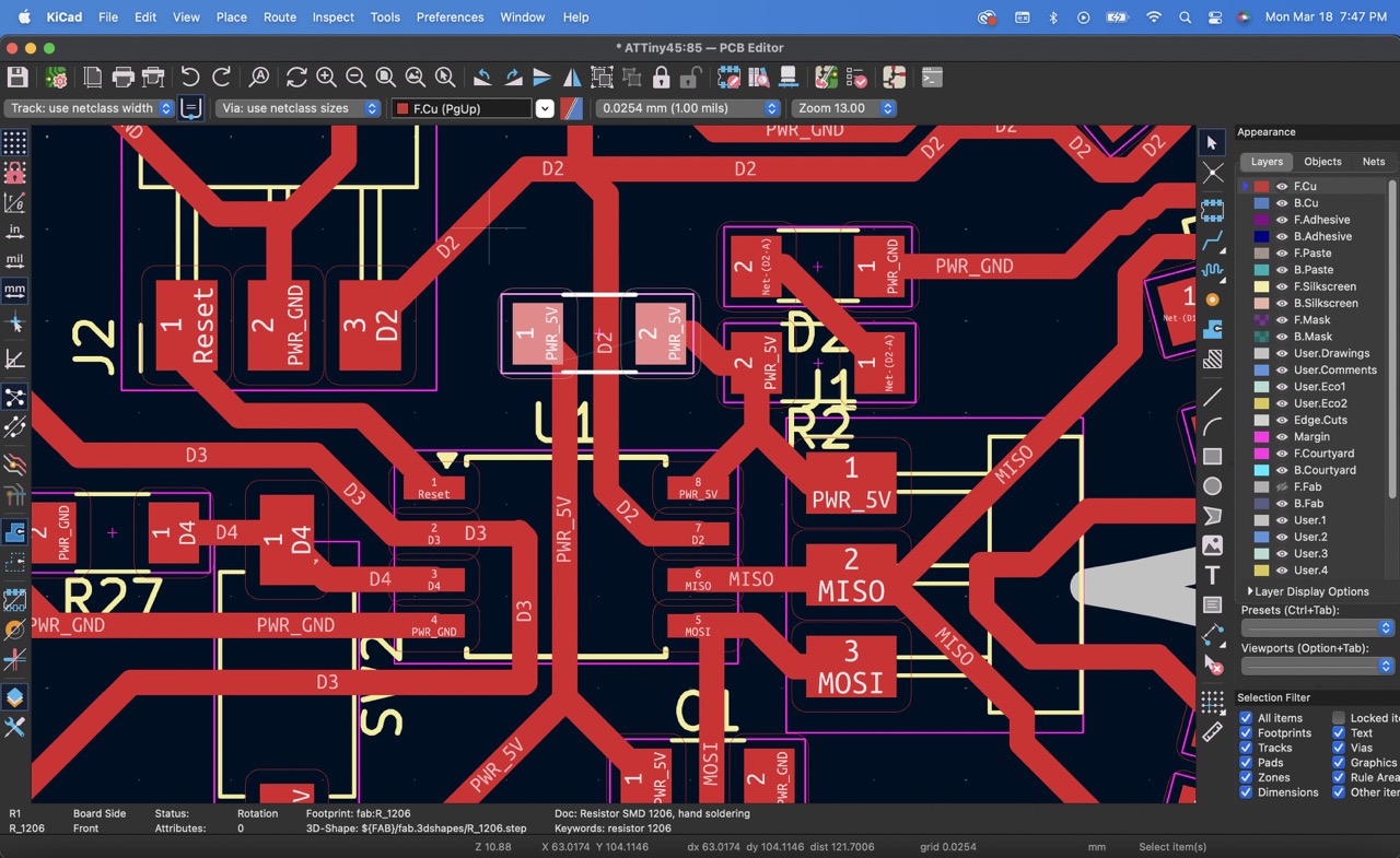
6:
Under the 'File' drop-down menu, I selected ‘Board Setup’ and modified certain parameters in the 'Constraints' under ‘Design Rules’. I set the minimum clearance to 0.4 mm and the minimum track width to 0.7 mm.
7:
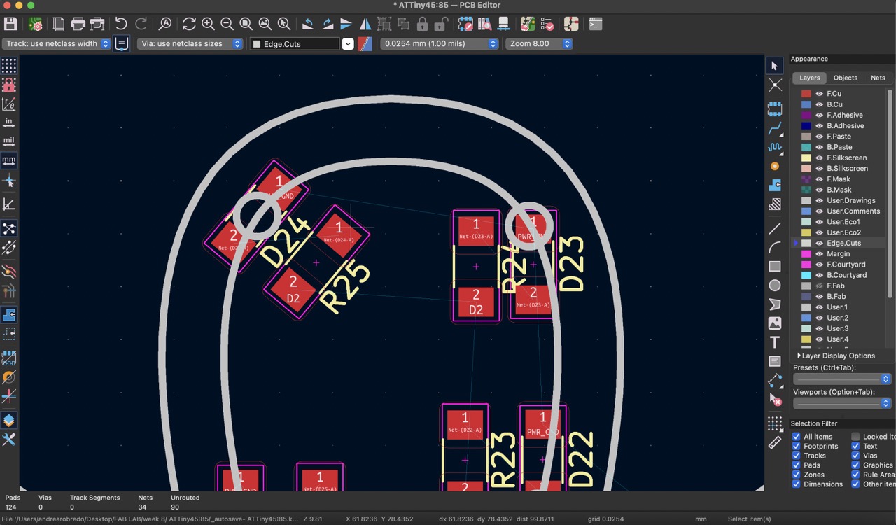
With these settings configured, I began creating the route tracks by activating the 'x' key tool. This tool visually indicates which components should be connected.
8:
There came a point where I needed to create a bridge (resistor 0) because it wasn't possible to directly connect both the LEDs attached to D2 and the 5V supply from the button and capacitor due to intersection. To resolve this, I returned to the 'Schematic Editor', added a new resistor connected to 5V on both sides, updated the schematic in the 'PCB Editor', and positioned it as a bridge to connect the 5V.
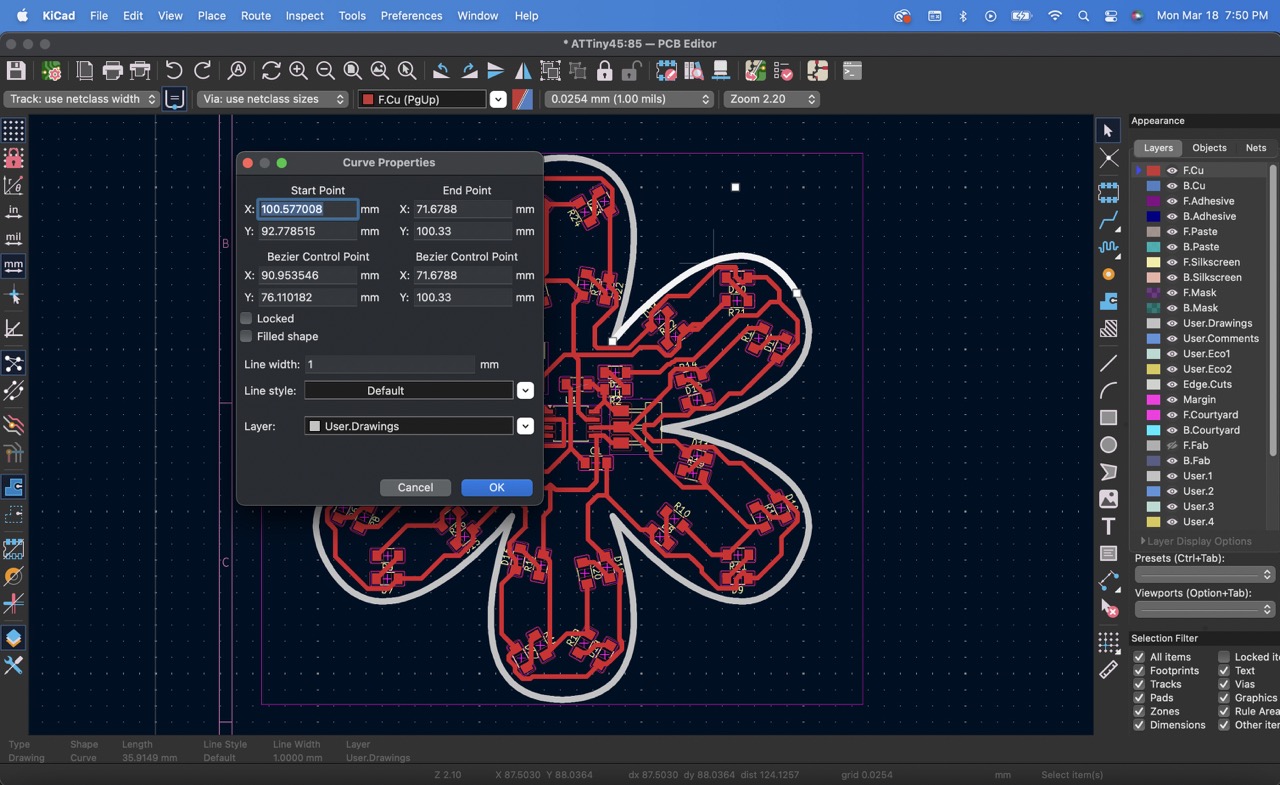
9:
Finally, after ensuring all connections were correct, I adjusted the outline to have a 1 mm line width by selecting the curve and pressing the ‘e’ key.
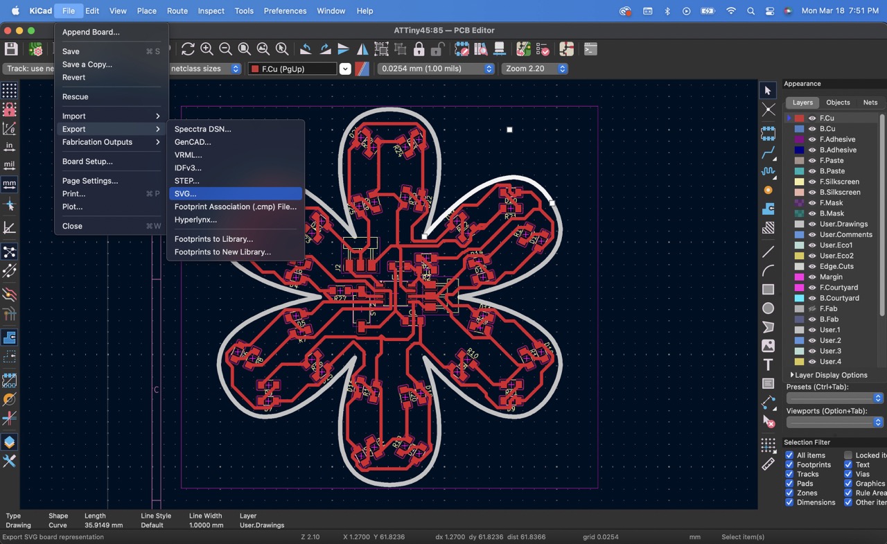
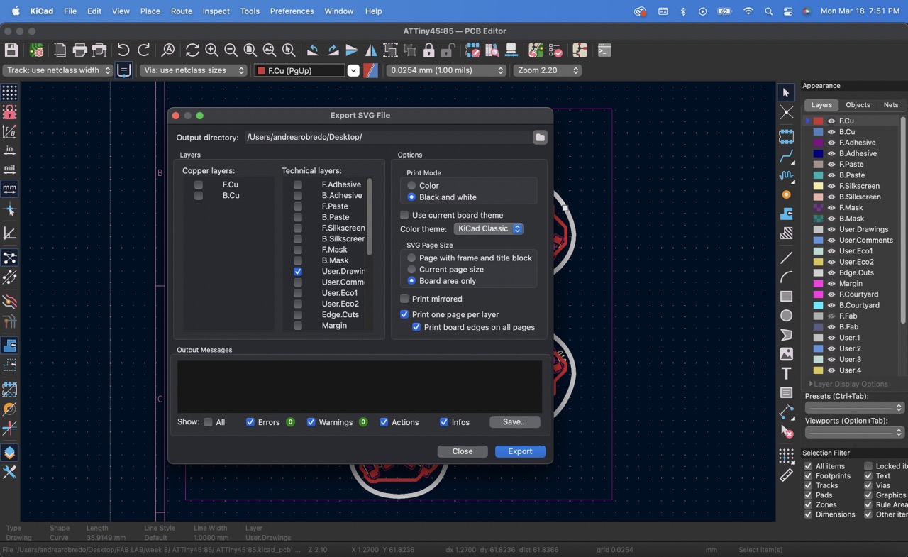
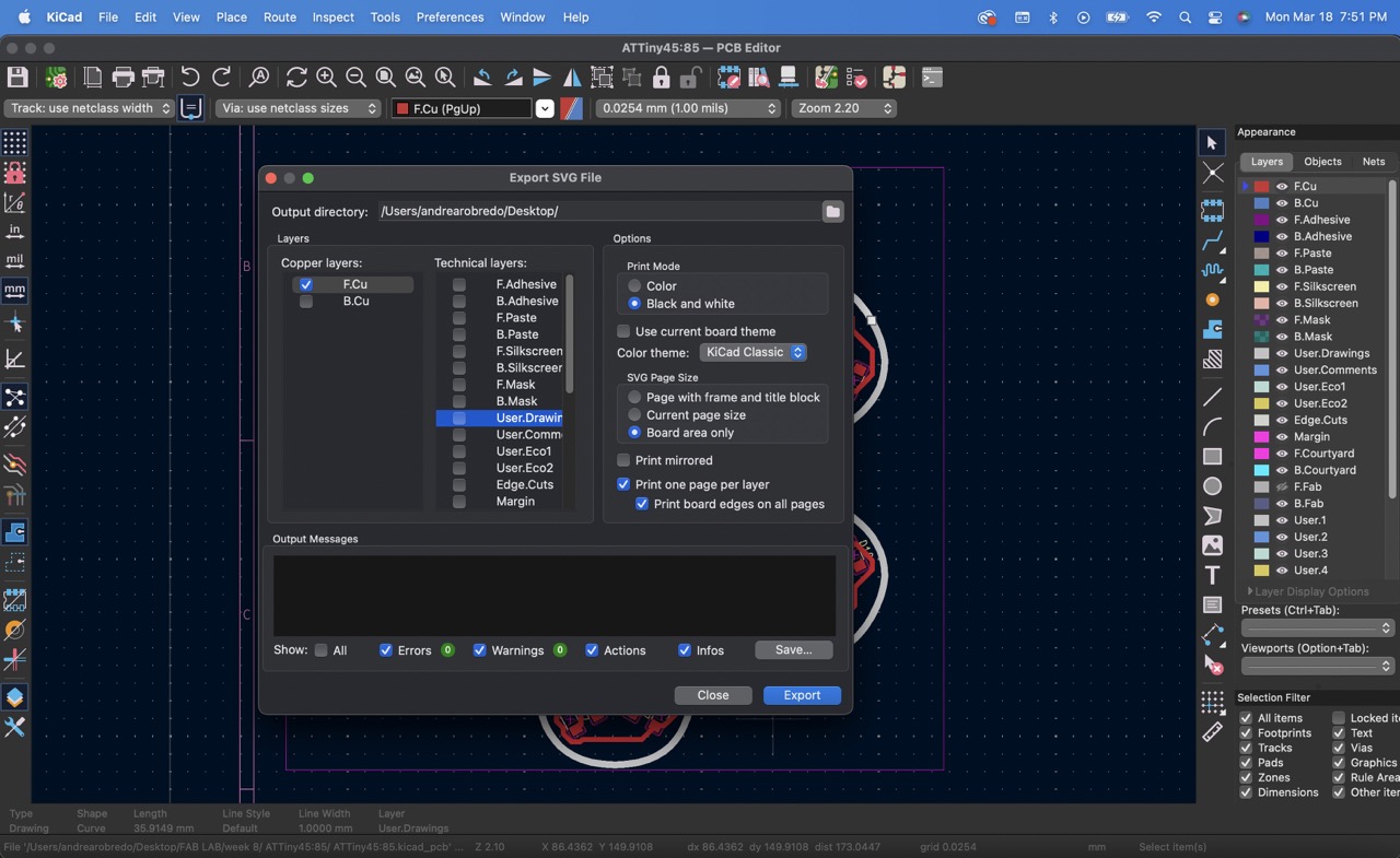
10:
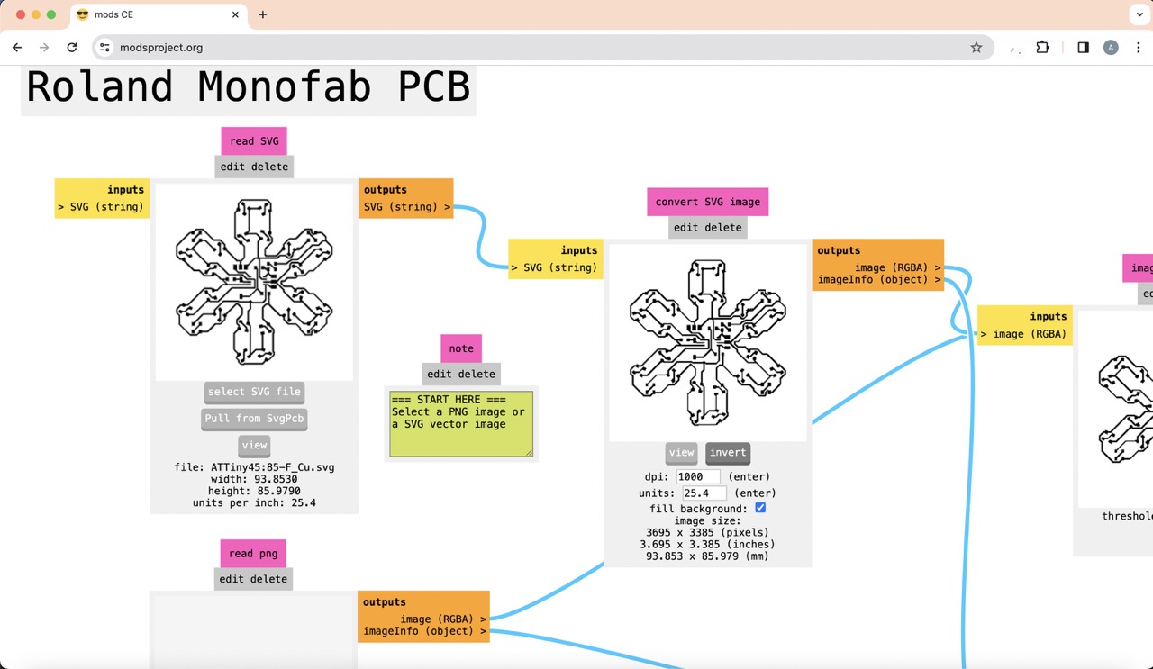
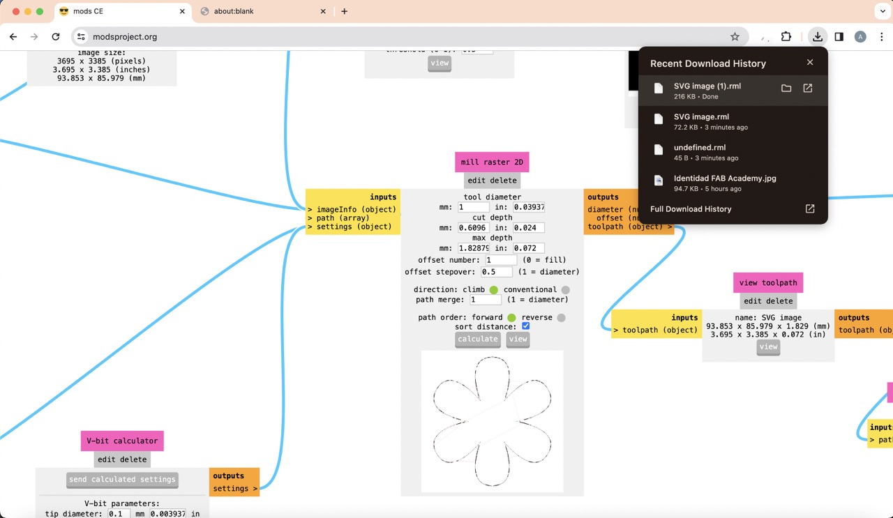
To finish, I exported the file as an SVG. For cutting purposes, I selected only the ‘User.Drawings’ layer, and for milling, I chose the ‘F.Cu’ copper layer.
Cutting PCB and soldering it
Files
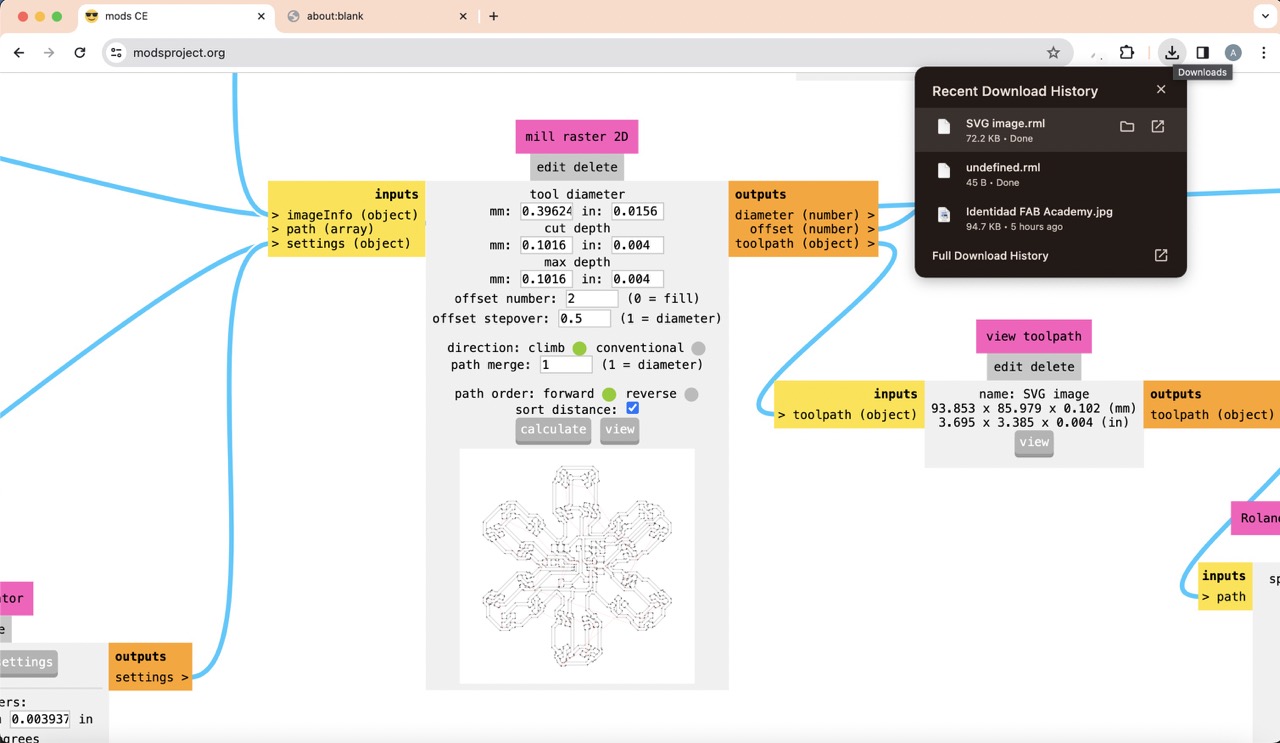
To generate the necessary files, I utilized MODs. Here's the process:
1:
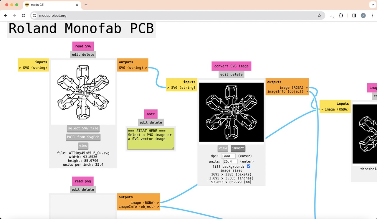
To start, I accessed the 'Programs' section, then 'Open Program', and searched for my milling machine, 'Roland SRM-20 mill', and specifically selected 'mill 2D PCB'. After importing the trace SVG, I inverted it to ensure that the white areas represent the paths, while the black areas indicate where cutting occurs.
2:
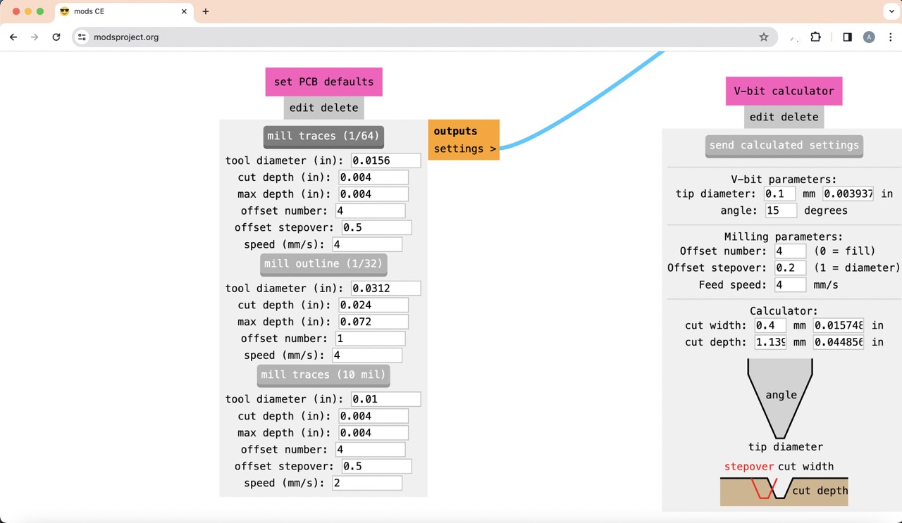
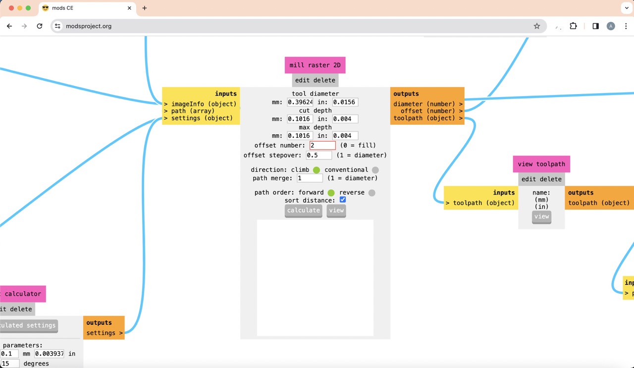
Then I selected ‘mill traces’ and adjusted the offset number to 2.
3:
I set the origin to 0,0,0 and activated the output file. Finally I clicked on the calculate button and immediately the file was downloaded.
4:
Now, to cut the outline I started by inserting the corresponding svg file.
5:
Clicked on 'mill outline'.
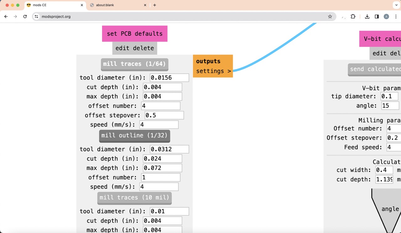
6:
Adjusted the tool diameter to 1 mm.
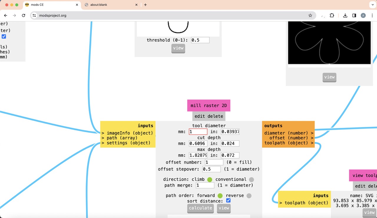
7:
Clicked the 'Calculate' button to obtain the cutting file.
For a more detailed explanation on how to use mods go to my week 4: electronics production documentation
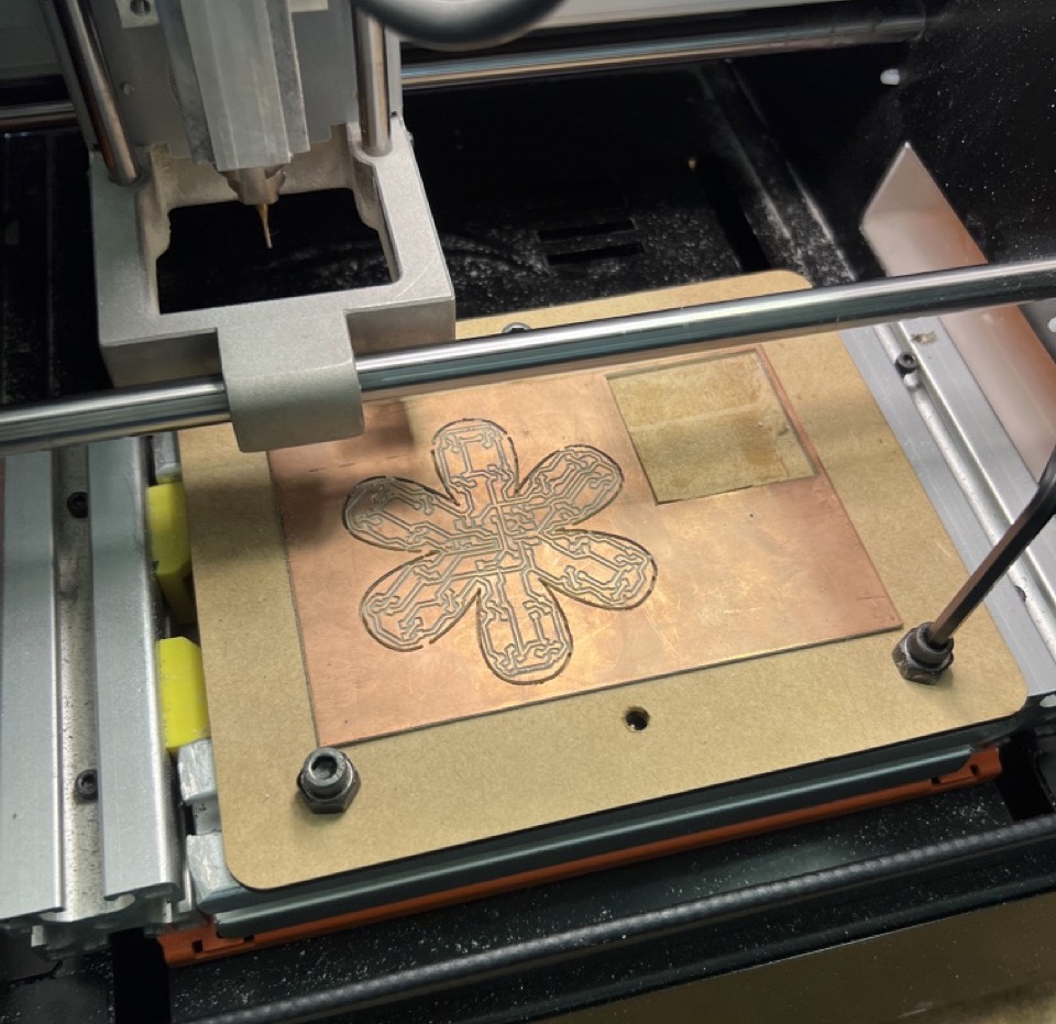
Milling
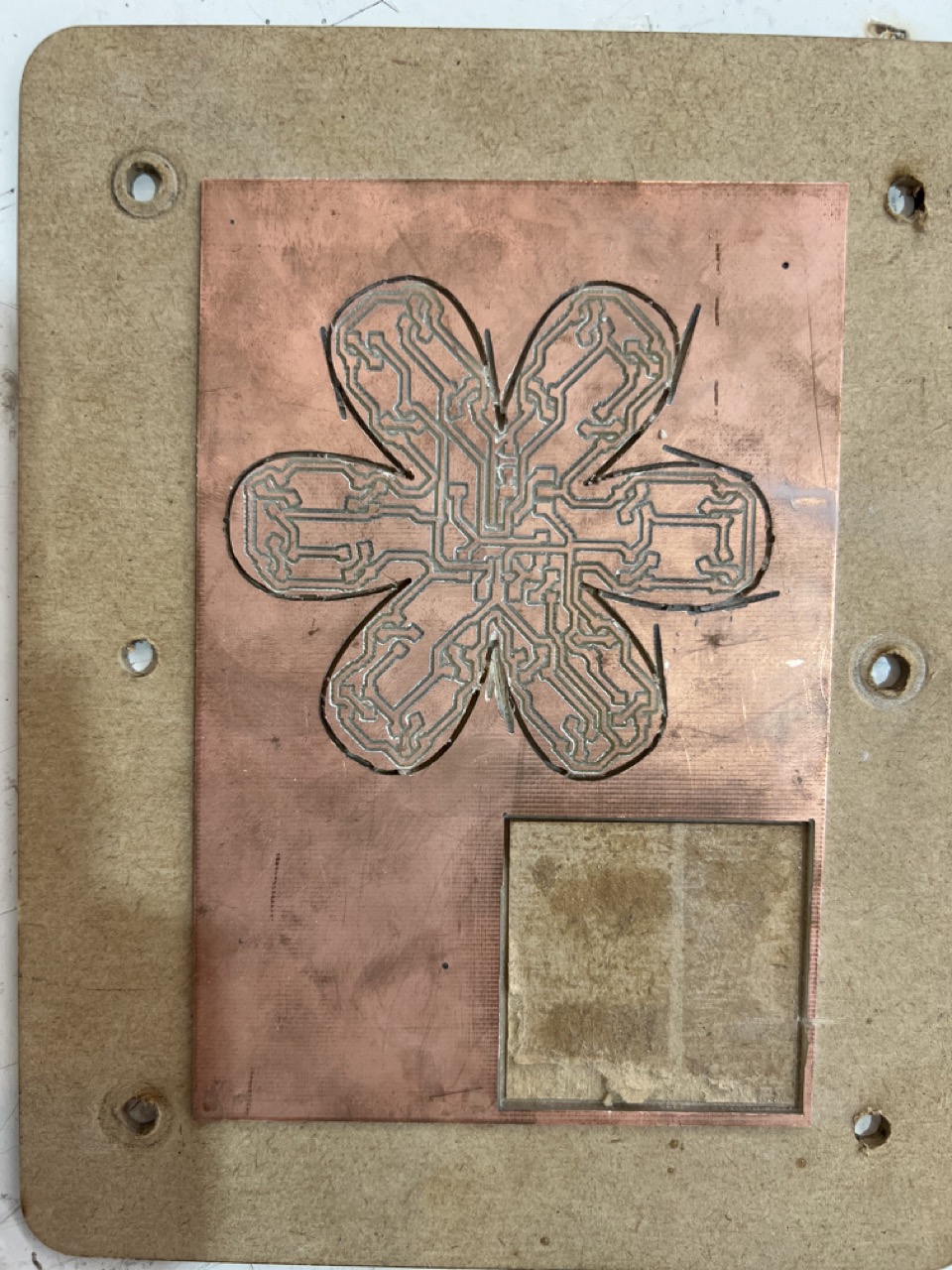
To begin, I secured the sacrificial board to the machine using screws. Then, using the Vpanel software, I established the x and y origin points at the lower-left corner. Afterward, I adjusted the z origin, lowering it slightly to accommodate the unevenness of the board. I then installed the engraving drill and loaded the trace file to start engraving.
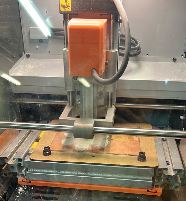
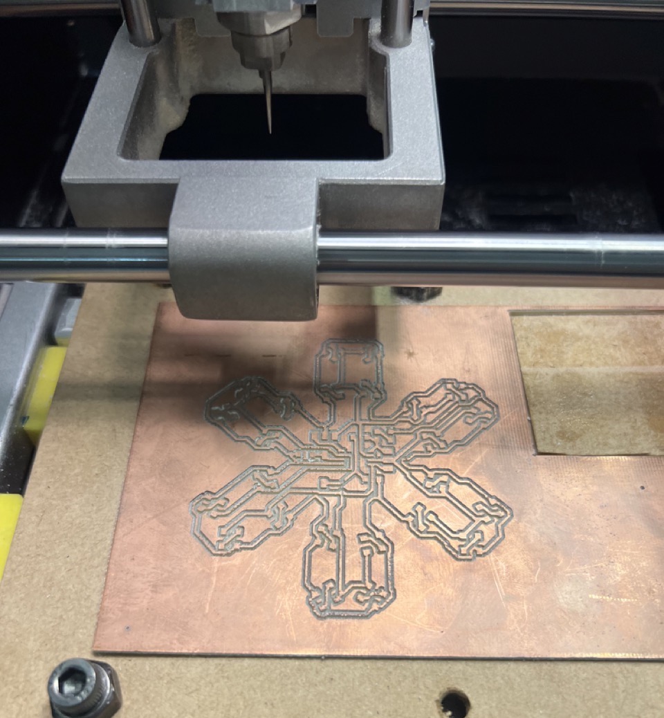
Once the engraving was completed, I switched to the cutting drill, readjusted the z origin, opened the corresponding file, and initiated the cutting process.
For a more detailed explanation on how to use the milling machine go to my week 4: electronics production documentation
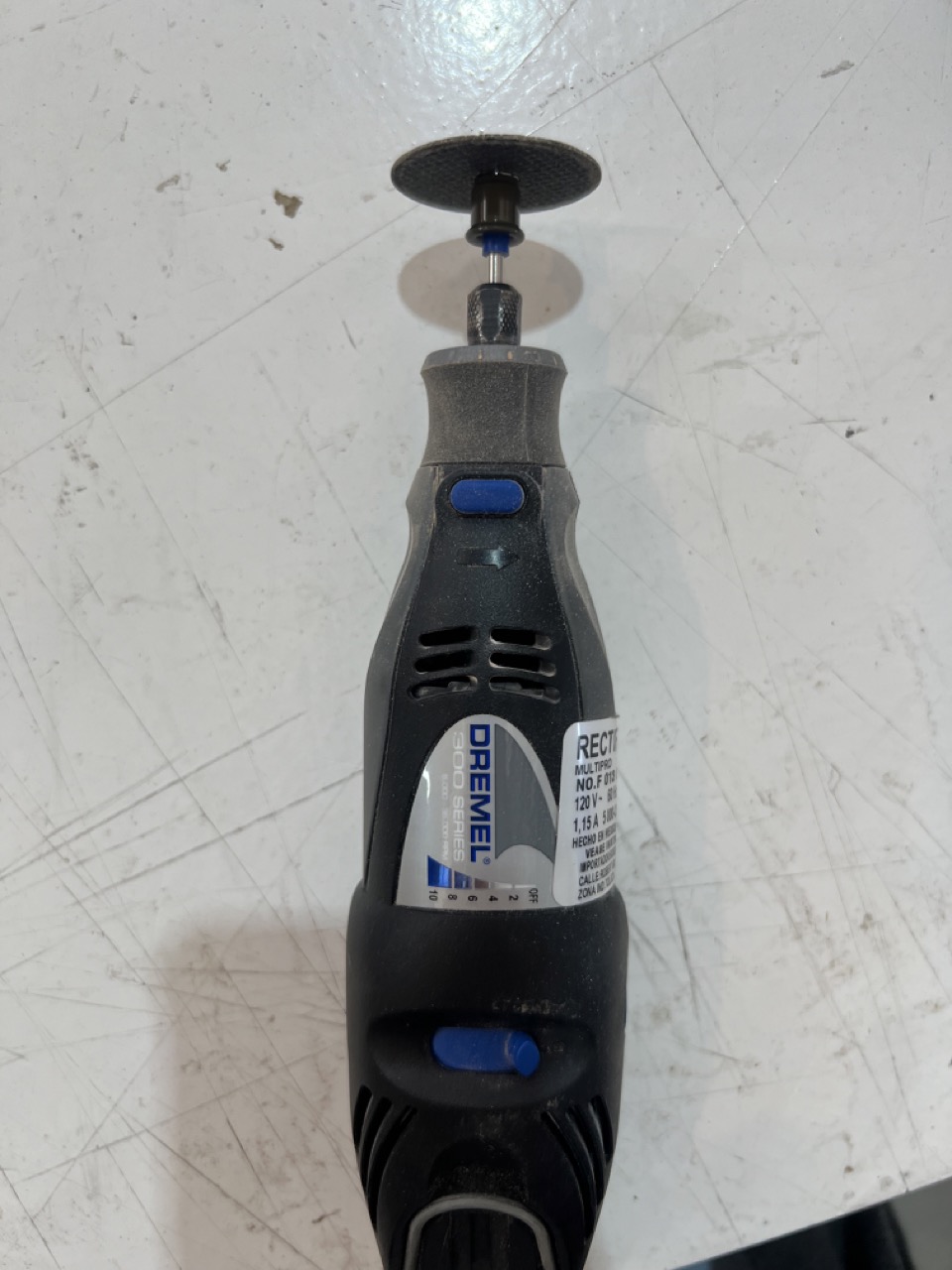
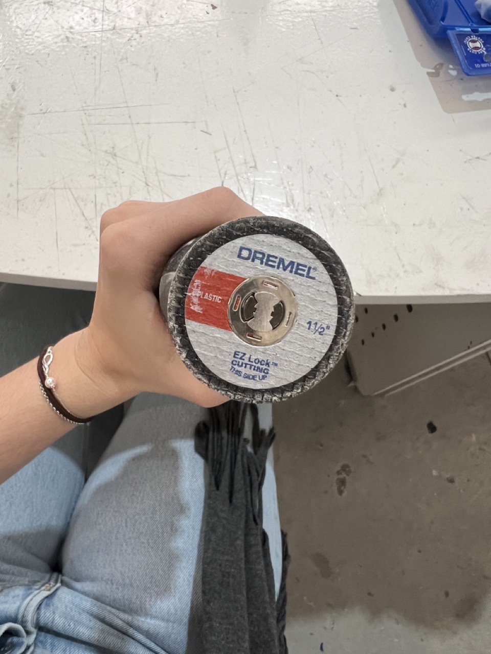
Due to some issues with the cutting file, I had to cut some uncut parts of the outline with a dremel.
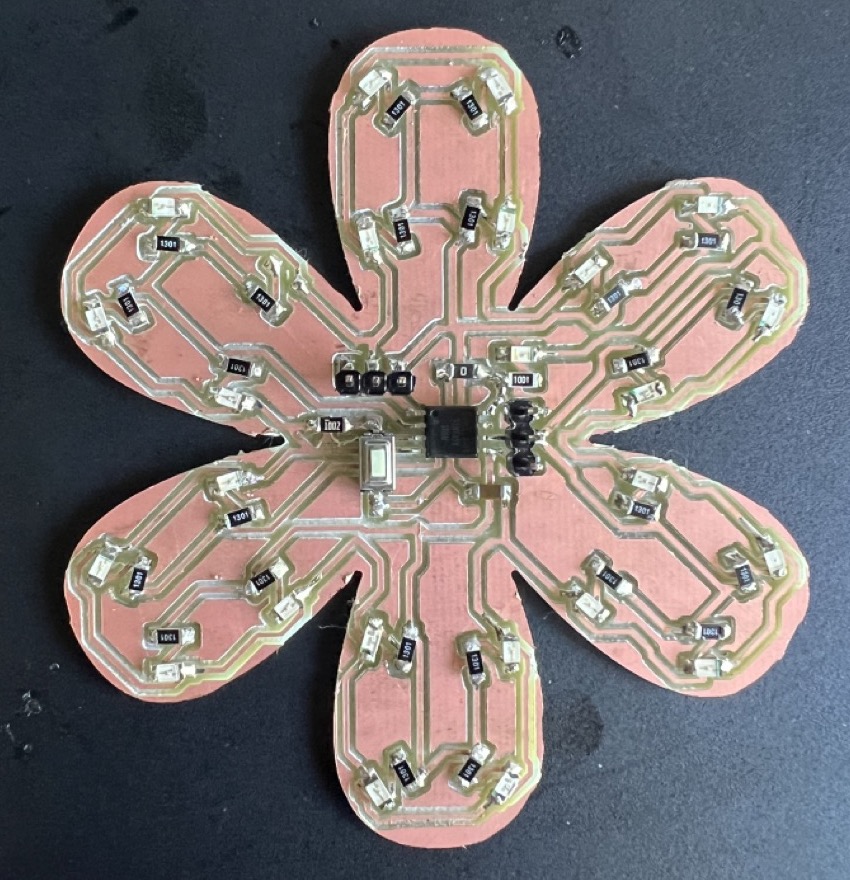
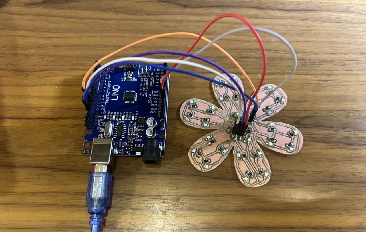
Soldering
Components needed
Component |
Quantity |
|---|---|
| ATtiny 85 | 1 |
| Red LED | 24 |
| Yellow LED | 1 |
| Resistor 1.3 k ohm | 24 |
| Resistor 0 ohm | 1 |
| Resistor 1 k ohm | 1 |
| Resistor 10 k ohm | 1 |
| Button | 1 |
| Capacitor | 1 |
| Pins | 2 (3 pin bed) |
First, I started by soldering the resistors.
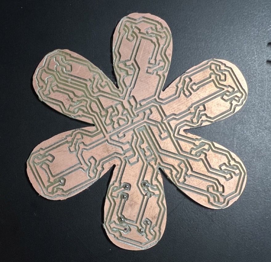
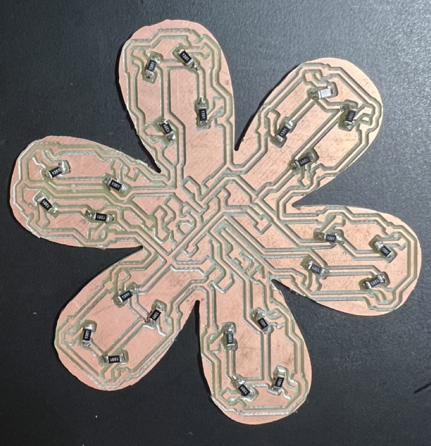
Then, I moved on to solder the inside components.
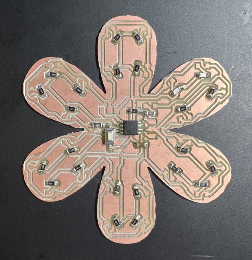
Finally, I soldered the LEDs located on the petals.
Programming
I will be programming the ATtiny 45 with an Arduino Uno.
1:
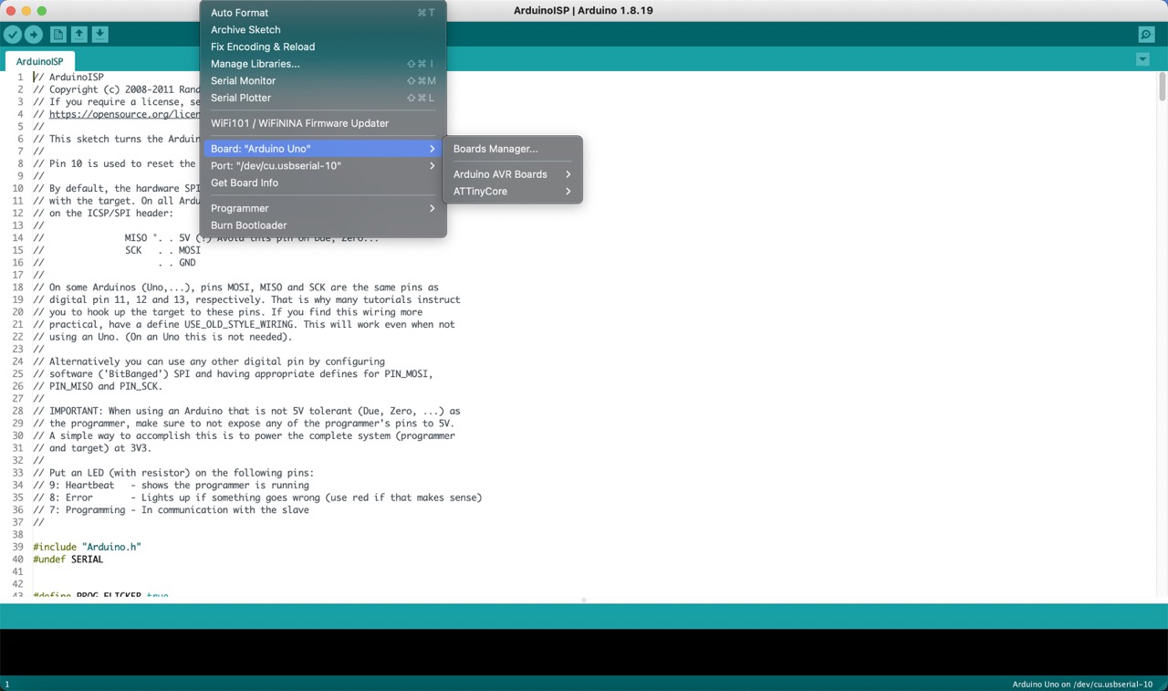
Connect your Arduino Uno to your computer and open the Arduino software. Go to 'File' > 'Examples' and select '11.ArduinoISP'.
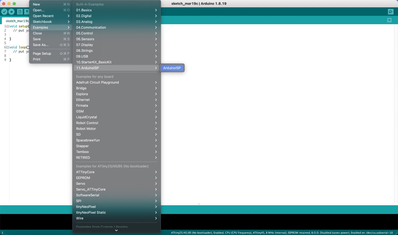
2:
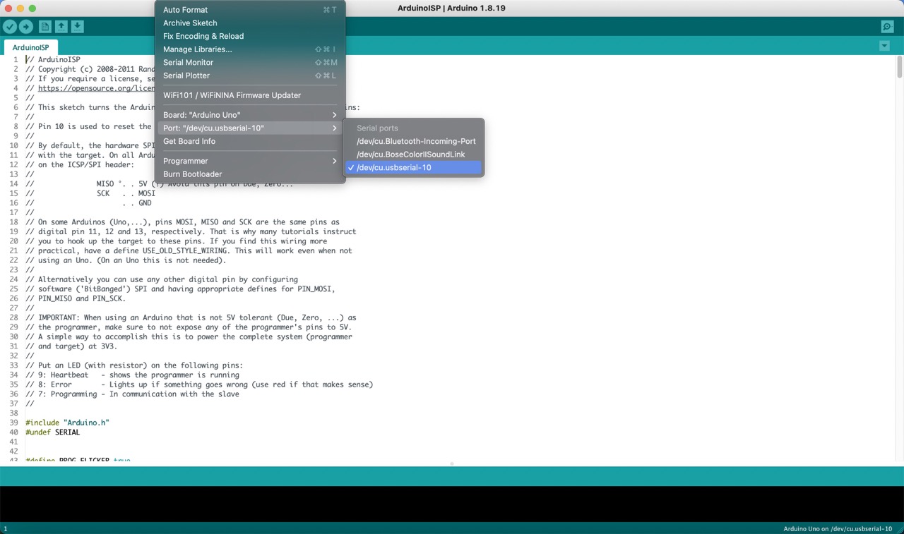
Make sure that under 'Tools' the 'Board' selected is 'Arduino Uno' as well as the correct 'Port'.
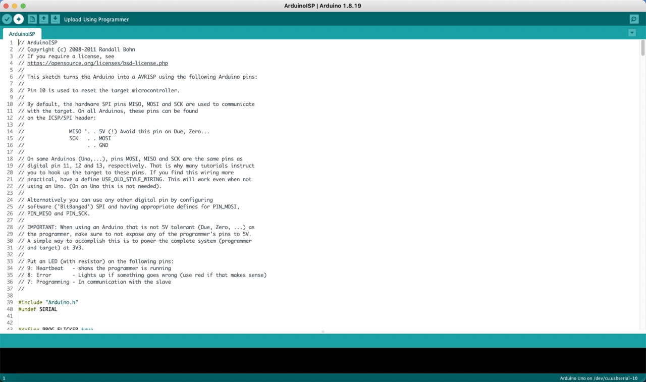
3:
Upload the code to your Arduino Uno and wait for it to finish uploading.
4:
Once uploaded successfully, open the code you want to program onto the ATtiny.
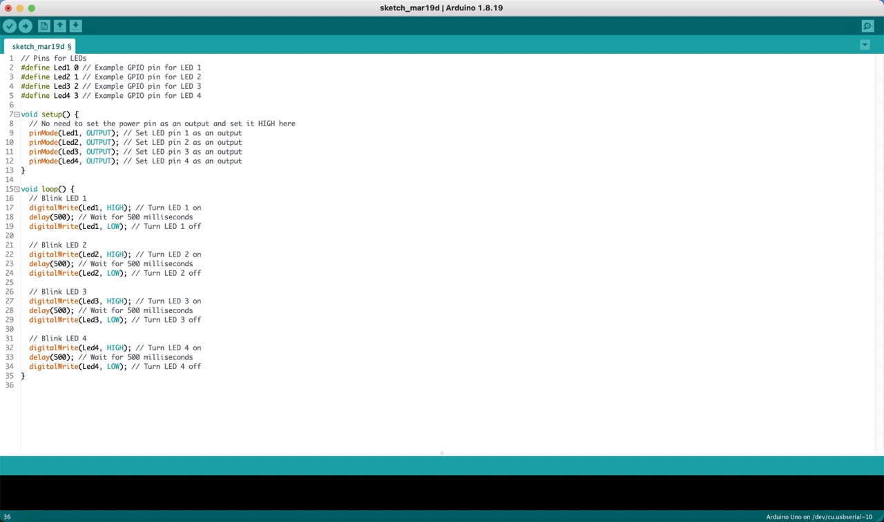
5:
Use the following schematic to connect your ATtiny pins to the Arduino Uno.
6:
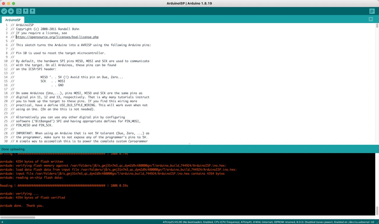
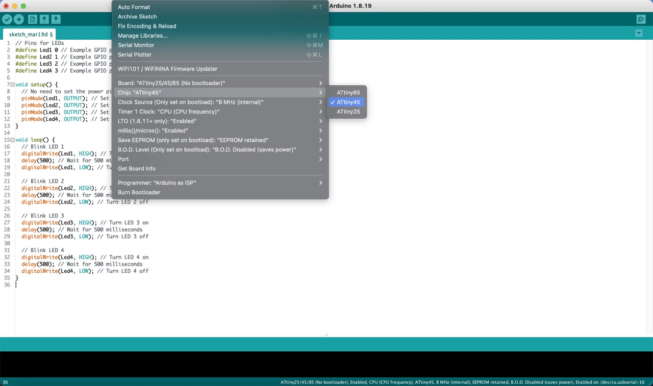
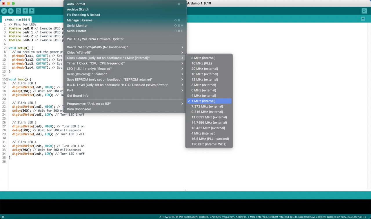
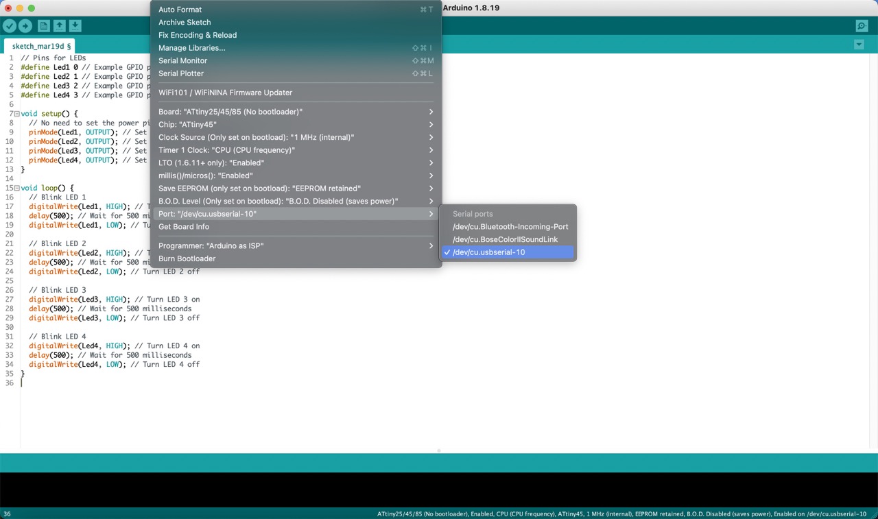
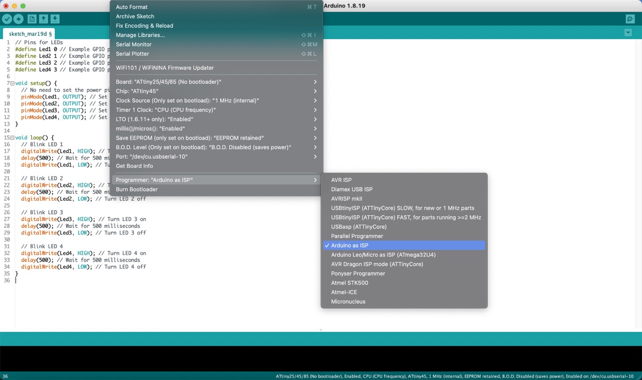
Under 'Tools', change the 'Board' to 'ATtiny 25/45/85 (No bootloader)'. Select 'ATtiny45' as the 'Chip', choose '1MHz (internal)' as the 'Clock Source', and ensure the correct 'Port' is selected. For 'Programmer', choose 'Arduino as ISP'.
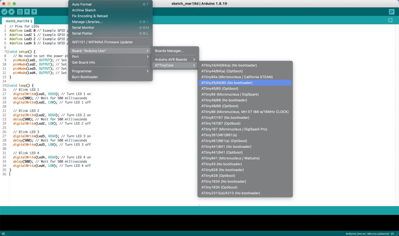
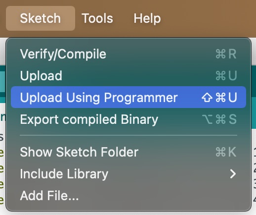
7:
Then, go to 'Sketch' and select 'Upload using programmer'.
8:
Done:)