Week 06: Embedded Programming
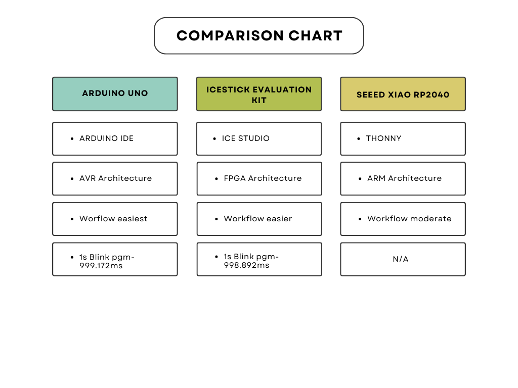
Week 6 group assignment is to browse through the data sheet of our microcontroller Seeed XIAO RP2040 and compare the performance and development workflows for other architectures.
Embedded Systems
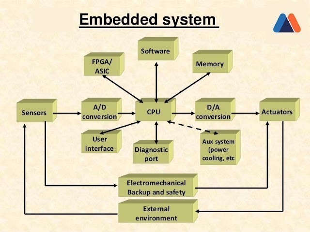
Embedded systems are specialized computer hardware systems programmed to execute specific tasks, ranging from simple to complex functions. They utilize microcontrollers, DSPs, ASICs, or FPGAs for real-time processing. These systems interact with the environment through sensors, which convert physical signals to electrical ones. Analog-to-digital converters then translate these signals for processing by the system’s processor. After computation, digital-to-analog converters convert the processed data back to analog form. Actuators act upon this output, adjusting it as necessary. This structured approach enables embedded systems to perform their designated functions efficiently, spanning applications from consumer electronics to automotive and aerospace industries.
Microcontrollers
Microcontrollers are compact computing devices integrated onto a single chip, designed to execute specific tasks within embedded systems. They encompass a microprocessor core, memory, and various input/output peripherals. These devices are commonly found in a diverse range of applications, including consumer electronics, automotive systems, industrial automation, medical devices, and IoT devices. With low power consumption and real-time operation capabilities, microcontrollers are well-suited for battery-powered and time-sensitive applications. Programming microcontrollers involves using specialized development tools and languages such as C, C++, and assembly language. Their small size, cost-effectiveness, and ability to perform dedicated functions make them indispensable in modern technology. As technology advances, microcontrollers continue to evolve, offering increased processing power, enhanced connectivity options, and improved energy efficiency. In summary, microcontrollers are fundamental components in embedded systems, playing a vital role in powering numerous electronic devices and driving innovation across various industries.
RP2040 datasheet
The RP2040 datasheet is a comprehensive document provided by Raspberry Pi detailing the specifications, features, and electrical characteristics of the RP2040 microcontroller chip. Developed by Raspberry Pi, the RP2040 is a powerful microcontroller featuring dual ARM Cortex-M0+ cores and a rich set of peripherals.
Contents
The RP2040 datasheet includes the following sections:
- Introduction:
The post-fix numeral on RP2040 comes from the following,
- Number of processor cores (2)
- Loosely which type of processor (M0+)
- floor(log2(ram / 16k))
- floor(log2(nonvolatile / 16k)) or 0 if no onboard nonvolatile storage
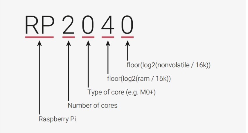
The RP2040, reflecting Raspberry Pi’s ethos of accessibility and cost-effectiveness, is a versatile microcontroller suitable for a wide array of projects. Supporting both C/C++ and MicroPython, it features dual Cortex M0+ cores, ample SRAM, multifunction GPIO, and dedicated hardware for peripherals. With built-in USB capabilities functioning as both device and host, it offers flexibility in connectivity. Its high internal bandwidth and four-channel ADC with an internal temperature sensor enable efficient signal processing. The chip’s naming convention derives from its core count, type, RAM, and nonvolatile storage, underscoring its integrated features and customizable memory options for tailored applications.
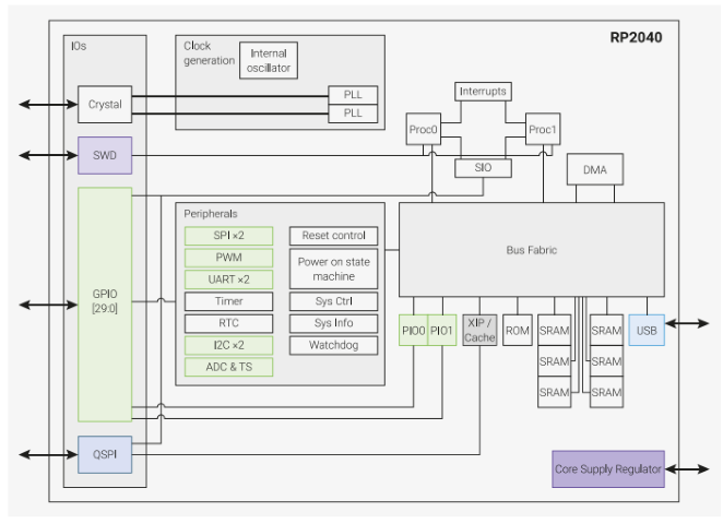
- Pinout Diagram:
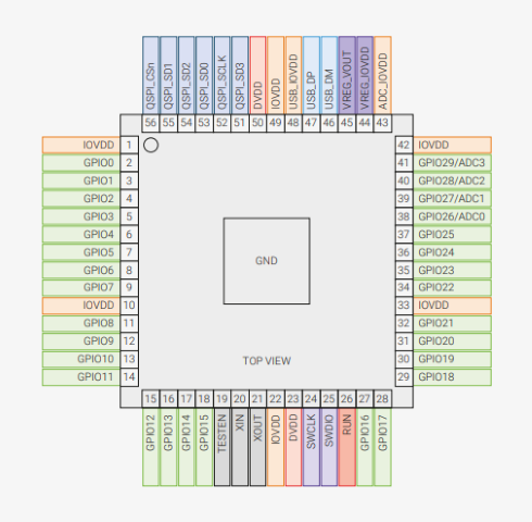
- Power Supply Pins
- VDD: Core power supply pins.
- VSYS: System power supply pin, which can be in the range of 1.8V to 5.5V.
- 3V3_EN: 3.3V regulator enable pin.
- 3V3_OUT: Output from the onboard 3.3V regulator.
- GND: Ground pins.
- Clock Pins
- XTAL_IN and XTAL_OUT: Pins for connecting an external crystal oscillator.
- GPIO: General Purpose Input/Output pins, some of which can be configured for specific functions (e.g., I2C, SPI, UART) or used for PWM, digital read/write, analog read, etc.
- Communication Interface Pins
- SPI: Serial Peripheral Interface pins for SPI communication.
- I2C: Pins for I2C communication.
- UART: Universal Asynchronous Receiver/Transmitter pins for serial communication.
- USB D+ and USB D-: USB data pins for connecting the RP2040 to a computer or other USB host.
- ADC (Analog to Digital Converter) Pins
- Specific GPIO pins can also serve as ADC inputs for reading analog voltages.
-
Debugging Pins
- SWCLK and SWDIO: Serial Wire Debug (SWD) clock and data pins for programming and debugging the microcontroller.
-
Electrical Characteristics: Electrical specifications such as voltage levels, current ratings, and operating conditions.
- IOVDD: Power supply for digital GPIOs, nominal voltage 1.8 V to 3.3 V
- USB_IOVDD: Power supply for internal USB Full Speed PHY, nominal voltage 3.3 V
- ADC_IOVDDD: Power supply for analogue-to-digital converter, nominal voltage 3.3 V
- VREG_IOVDD: Power input for the internal core voltage regulator, nominal voltage 1.8 V to 3.3 V
- VREG_VOUT: Power output for the internal core voltage regulator, nominal voltage 1.1 V, 100 mA max current
- DVDD: Digital core power supply, nominal voltage 1.1 V. Can be connected to VREG_VOUT, or to some other board-level power supply
-
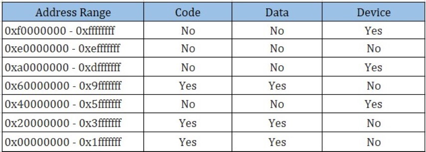
Memory Map: The memory map in the context of an ARMv6-M architecture-compliant system, such as the RP2040 or other microcontrollers using the ARM Cortex-M0+ processor, outlines how the system’s memory space is organized and accessed both by the processor and the debugger. This setup ensures efficient management of memory resources, prioritizes processor access to maintain performance during debugging, and delineates specific memory regions for different types of transactions. Here’s a concise summary of the key aspects:
-
AHB-Lite Master Port Transactions: Memory accesses that fall below 0xd0000000 or above 0xefffffff in the address space are routed as AHB-Lite transactions through the processor’s AHB-Lite master port. This interface is designed for high-bandwidth data transfers within the system, catering to the core and peripheral communications.
-
SIO Handling: Accesses within the 0xd0000000 to 0xdfffffff range are managed by the Serial Input/Output (SIO) block. This segment typically involves direct memory access (DMA) operations and peripheral control, facilitating efficient data movement and device management without engaging the CPU for every transaction.
-
Internal Processor Handling: The address range from 0xe0000000 to 0xefffffff is reserved for internal processor functions, including the Nested Vectored Interrupt Controller (NVIC) and debug components. These accesses do not appear on the AHB-Lite master port, ensuring that critical system and debug operations are isolated from general memory transactions.
-
Bus Matrix and Debug Access Port (DAP): The processor incorporates a bus matrix to arbitrate between the processor core and Debug Access Port memory accesses, targeting both external memory systems and internal components like the NVIC and debug modules. The design prioritizes processor access to ensure minimal disruption during debug operations, aiming for a zero wait-state system where debug accesses do not interfere with normal code execution.
-
Memory Protection Unit (MPU): While the base memory map provides a default organization and access permissions, the presence of an MPU allows for further customization. Except for regions dedicated to the Cortex-M0+ NVIC and debug components, the MPU can adjust the attributes and permissions of memory regions, enhancing system security and stability by controlling access to sensitive areas.
-
Peripheral Descriptions:
- USB: RP2040 contains a USB 2.0 controller that can operate as either:
- a Full Speed device (12 Mbit/s)
- a host that can communicate with both Low Speed (1.5 Mbit/s) and Full Speed devices. This includes multiple downstream devices connected to a USB hub.
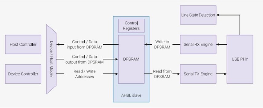
There is an integrated USB 1.1 PHY which interfaces the USB controller with the DP and DM pins of the chip. The USB controller hardware handles the low level USB protocol, meaning the main job of the programmer is to configure the controller and then provide / consume data buffers in response to events on the bus. The controller interrupts the processor when it needs attention. The USB controller has 4K of DPSRAM which is used for configuration and data buffers
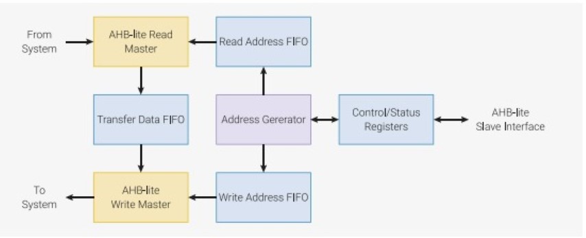
- DMA: The RP2040 Direct Memory Access (DMA) master performs bulk data transfers on a processor’s behalf. This leaves processors free to attend to other tasks, or enter low-power sleep states. The data throughput of the DMA is also significantly higher than one of RP2040’s processors
-
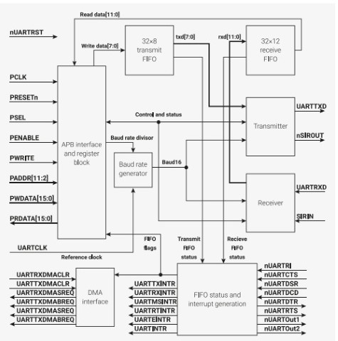
UART: RP2040 has 2 identical instances of a UART peripheral, based on the ARM Primecell UART (PL011) (Revision r1p5).
Each instance supports the following features:
• Separate 32x8 Tx and 32x12 Rx FIFOs
• Programmable baud rate generator, clocked by clk_peri (see Figure 26)
• Standard asynchronous communication bits (start, stop, parity) added on transmit and removed on receive
• line break detection
• programmable serial interface (5, 6, 7, or 8 bits)
• 1 or 2 stop bits
• programmable hardware flow control
Each UART can be connected to a number of GPIO pins as defined in the GPIO muxing table in Section 2.18.2. Connections to the GPIO muxing are prefixed with the UART instance name uart0_ or uart1_, and include the following:
• Transmit data tx
UART 439
• Received data rx
• Output flow control rts
• Input flow control cts
The modem mode and IrDA mode of the PL011 are not supported.
The UARTCLK is driven from clk_peri, and PCLK is driven from the system clock clk_sys
-
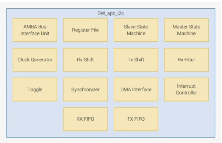
I2C : I2C is a commonly used 2-wire interface that can be used to connect devices for low speed data transfer using clock SCL and data SDA wires. RP2040 has two identical instances of an I2C controller. The external pins of each controller are connected to GPIO pins as defined in the GPIO muxing table in Section 2.18.2. The muxing options give some IO flexibility.
-
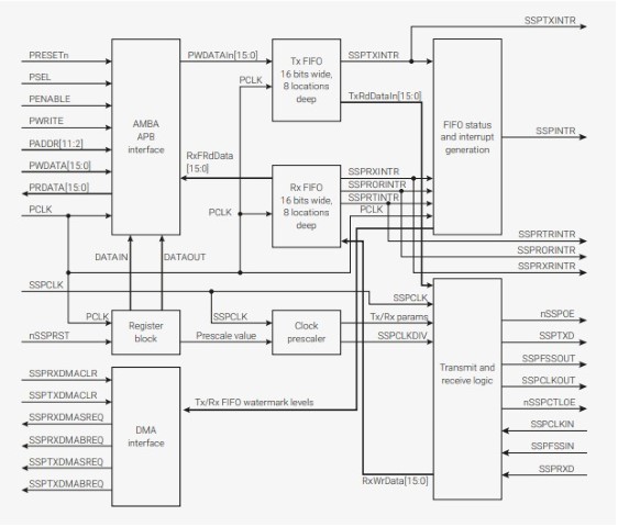
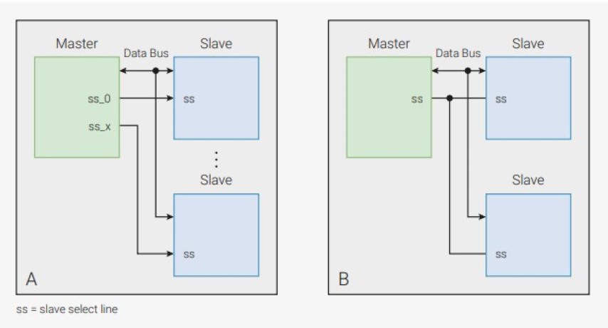
SPI : RP2040 has two identical SPI controllers, both based on an ARM Primecell Synchronous Serial Port (SSP) (PL022) (Revision r1p4). Note this is NOT the same as the QSPI interface covered in section SSI. Each controller supports the following features:
• Master or Slave modes
◦ Motorola SPI-compatible interface
- USB: RP2040 contains a USB 2.0 controller that can operate as either:
-
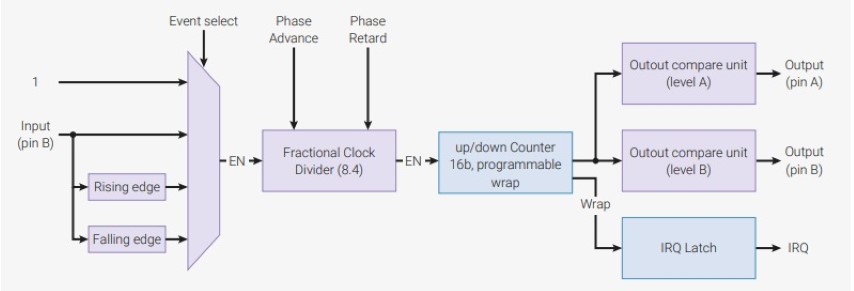
PWM : Pulse width modulation (PWM) is a scheme where a digital signal provides a smoothly varying average voltage. This is achieved with positive pulses of some controlled width, at regular intervals. The fraction of time spent high is known as the duty cycle. This may be used to approximate an analog output, or control switchmode power electronics. The RP2040 PWM block has 8 identical slices. Each slice can drive two PWM output signals, or measure the frequency or duty cycle of an input signal. This gives a total of up to 16 controllable PWM outputs. All 30 GPIO pins can be driven by the PWM block.
-
Timer : The timer peripheral on RP2040 supports the following features: • A single 64-bit counter, incrementing once per microsecond with the reference generated in the Watchdog (see Section 4.8.2).
• This counter can be read from a pair of latching registers, for race-free reads over a 32-bit bus.
• Four alarms: match on the lower 32 bits of counter, IRQ on match. Also note that each Cortex M0+ (see Cortex-M0+) is equipped with a 24-bit SysTick timer. This can be used to interrupt itself. The timer uses a one microsecond reference that is generated in the Watchdog (see Section 4.8.2) which comes from clk_ref
-
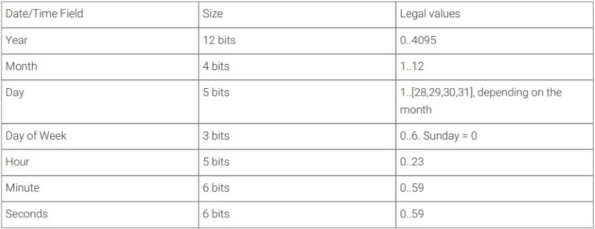
RTC : The Real-time Clock (RTC) provides time in human-readable format and can be set to generate events at specific times. Time is stored in binary, separated in seven fields. The RTC does not check values. Illegal values may cause unexpected behaviours. The RTC uses a reference clock clk_rtc, which should be set to any integer frequency in the range 1…65536 Hz. The internal 1 Hz reference is derived internally with an integer divider. Program the desired division value minus 1 through CLKDIV_M1. The clk_rtc can be driven either from an internal or external clock source. Those sources can be prescaled, using a fractional divider (see Clocks).
-
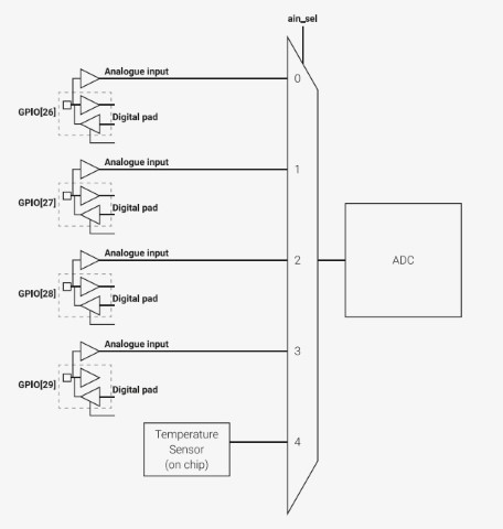
ADC and Temperature Sensor : RP2040 has an internal analogue-digital converter (ADC) with the following features:
• SAR ADC
• 500 kS/s (Using an independent 48MHz clock)
• 12-bit (9.5 ENOB)
• Five input mux:
Four inputs that are available on package pins shared with GPIO[29:26]
One input is dedicated to the internal temperature sensor RP2040 Datasheet
• Four element receive sample FIFO
• Interrupt generation
• DMA interface
- SSI : RP2040 has a Synchronous Serial Interface (SSI) controller which appears on the QSPI pins and is used to communicate with external Flash devices. The SSI forms part of the XIP block. The SSI controller is based on a configuration of the Synopsys DW_apb_ssi IP (v4.01a)
- Register Descriptions: The RP2040 is a microcontroller manufactured by Raspberry Pi. It uses the ARM Cortex-M0+ processor core. As such, it has various registers that control different aspects of its operation. Here’s a brief list of some of the commonly used registers:
General-Purpose Registers (R0-R12): These registers are used for general data manipulation and storage purposes during program execution.
Stack Pointer (SP): This register points to the current location in memory where the stack is located. It is used for storing temporary data and managing function calls.
Link Register (LR): This register stores the return address when a function is called, allowing the program to return to the correct location after the function completes execution.
Program Counter (PC): This register holds the memory address of the next instruction to be executed.
Status Registers (PSR, APSR, IPSR, EPSR): These registers store various status flags, such as the carry flag, zero flag, overflow flag, etc., which are used for controlling program flow and performing arithmetic operations.
Control Registers (CONTROL): This register controls the processor’s operation mode, including the privilege level and stack pointer selection.
System Control Registers (SCR): These registers control various system-level configurations, such as power management and interrupt handling.
NVIC Registers: These registers are used for configuring and controlling interrupts in the NVIC (Nested Vectored Interrupt Controller).
Peripheral Registers: The RP2040 has numerous peripheral modules, each with its own set of control and status registers for configuring and controlling the peripherals’ operation.
For detailed information on the registers and their usage, please refer to the RP2040’s datasheet.
-
Clocks and Timings: Information about clock sources, clock configurations, and timing specifications.
-
Power Management: Power supply requirements, power modes, and power consumption characteristics.
Importance
The RP2040 datasheet is an essential resource for engineers, developers, and hobbyists working with the RP2040 microcontroller. It provides detailed information needed for hardware design, firmware development, and troubleshooting. Understanding the specifications and capabilities of the RP2040 is crucial for effectively utilizing its features and building reliable systems.
Availability
The RP2040 datasheet is typically available for download from the Raspberry Pi website or the website of authorized distributors. It may be provided in PDF format or as part of a larger documentation package for the RP2040 development ecosystem.
In summary, the RP2040 datasheet is a vital document that serves as a comprehensive reference for anyone working with the RP2040 microcontroller, providing detailed information about its hardware features, electrical characteristics, and programming interfaces.
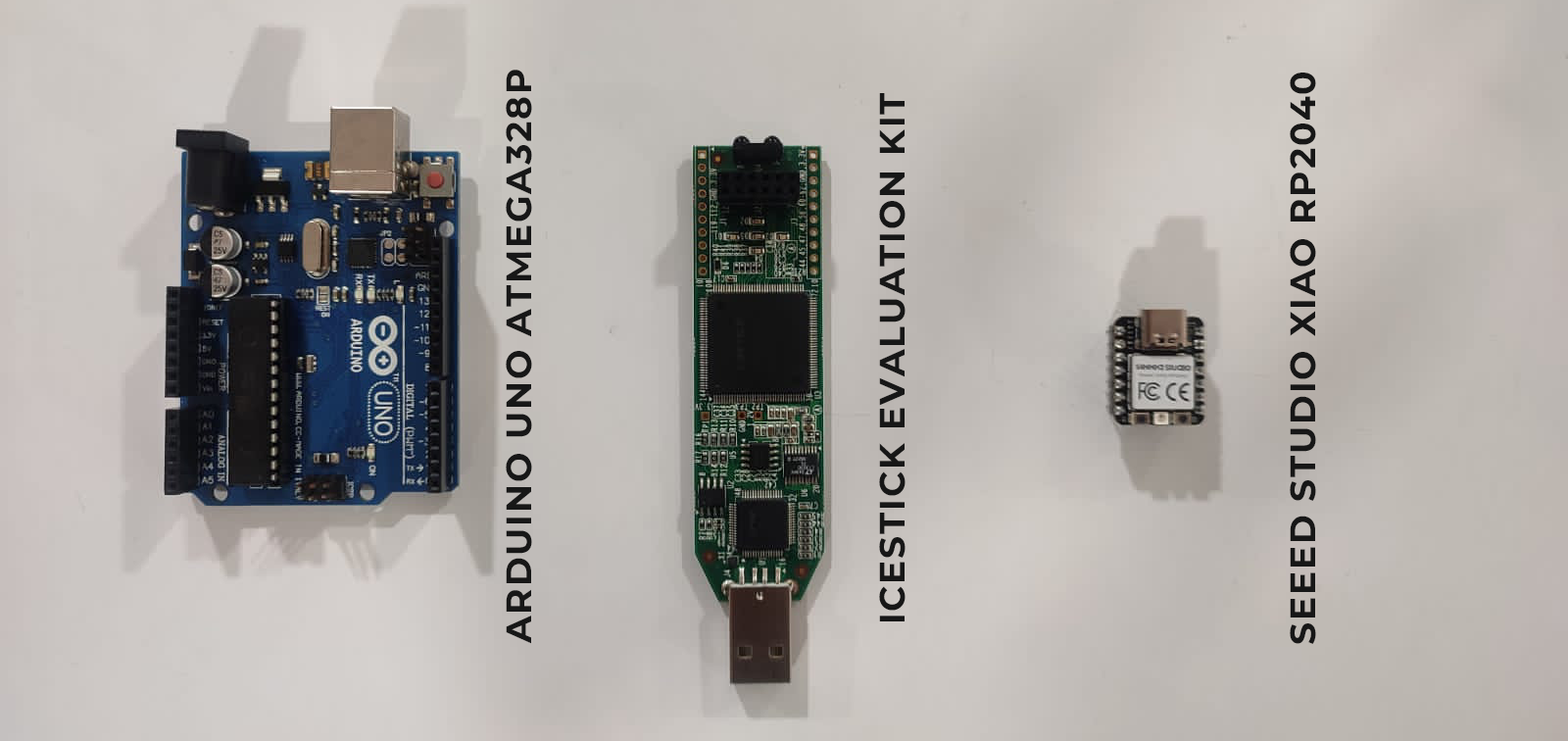
Seeed XIAO RP2040
The Seeed Xiao RP2040 is a compact microcontroller board based on the Raspberry Pi RP2040 microcontroller chip. Developed by Seeed Studio, this board offers a versatile and cost-effective solution for embedded projects.
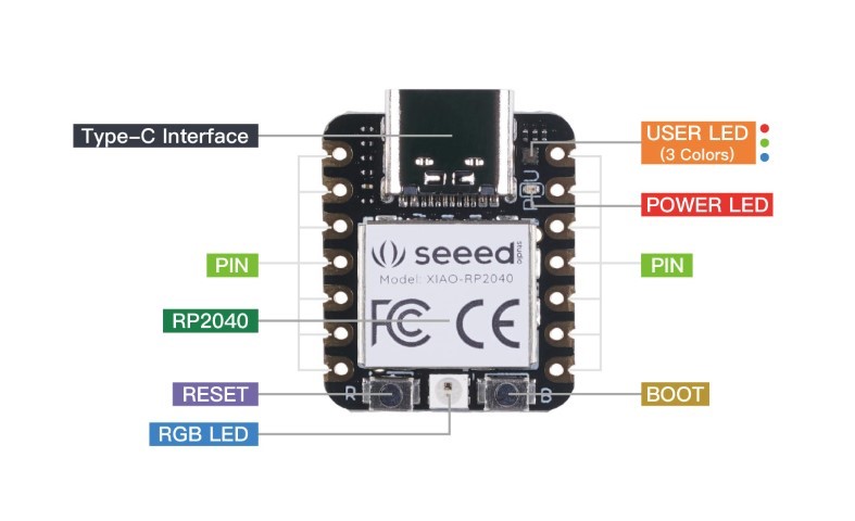
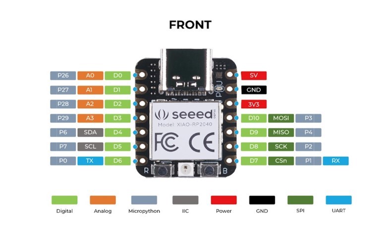
Key Features
-
Raspberry Pi RP2040 Chip: Powered by the RP2040 microcontroller chip, the Seeed Xiao RP2040 provides dual-core ARM Cortex-M0+ processors running at up to 133MHz, offering ample processing power for various applications.
-
Compact Form Factor: The board features a small form factor, making it suitable for projects with space constraints or where size is a consideration.
-
Rich Peripheral Set: Despite its small size, the Seeed Xiao RP2040 offers a rich set of peripherals, including GPIO pins, UART, I2C, SPI, PWM, ADC, and more, enabling interfacing with a wide range of sensors, actuators, and other devices.
-
USB-C Connectivity: The board features a USB-C connector for easy programming and power supply. It supports USB Mass Storage boot mode, allowing for easy drag-and-drop programming.
-
Arduino Compatibility: The Seeed Xiao RP2040 is Arduino-compatible, making it easy to program using the Arduino IDE and libraries, offering a familiar development environment for Arduino enthusiasts.
-
Open-Source Design: Like many Seeed Studio products, the Seeed Xiao RP2040 is an open-source hardware design, providing access to schematics, PCB layouts, and firmware source code for customization and community collaboration.
Workflow in MicroPython
Here are the steps to use the Seeed Xiao RP2040 with MicroPython using Thonny:
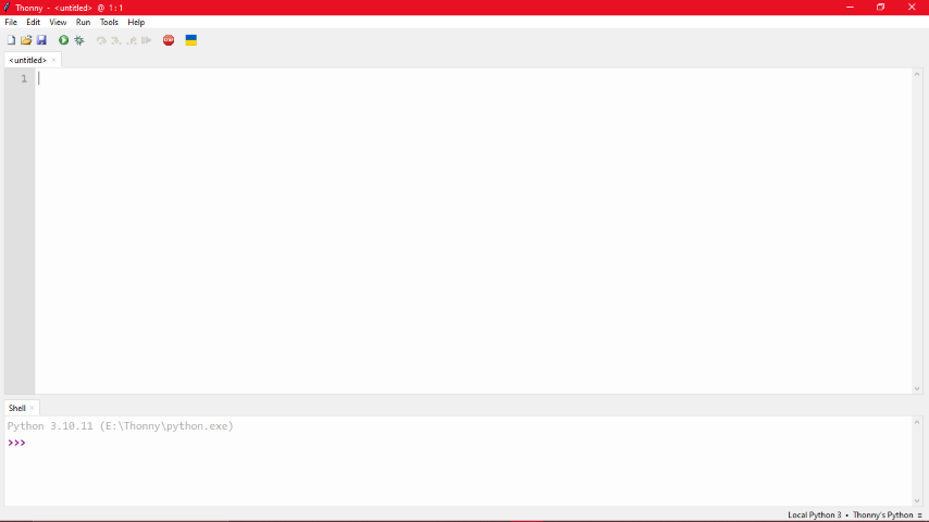
- Install Thonny IDE and launch it: Download and install Thonny IDE on your computer. Thonny is a Python IDE that’s beginner-friendly and supports MicroPython development. Launch the Thonny IDE on your computer.
-
Connect Seeed Xiao RP2040 to Computer: Use a USB cable to connect the Seeed Xiao RP2040 to PC by pressing and holding the boot button.
-
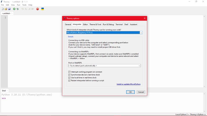
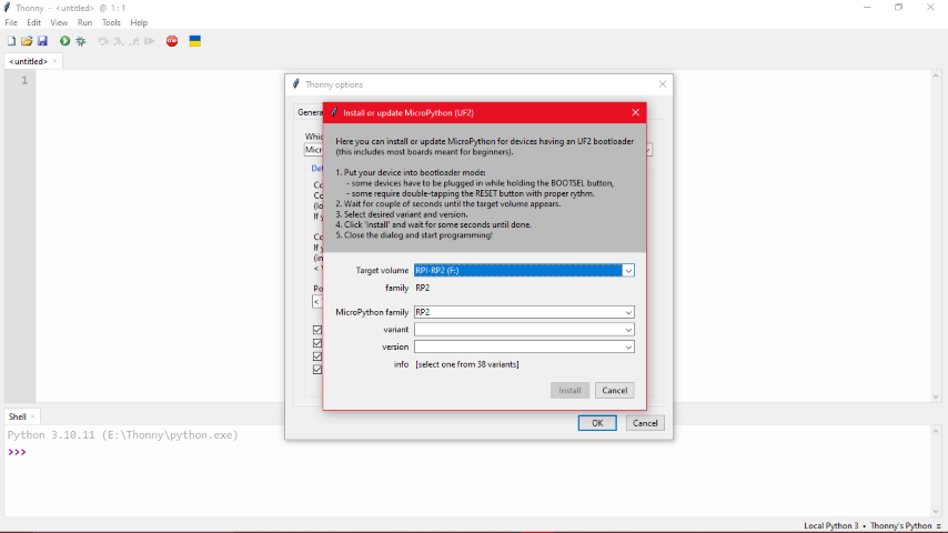
Download MicroPython Firmware: Download the MicroPython firmware for the Seeed Xiao RP2040 following these steps.
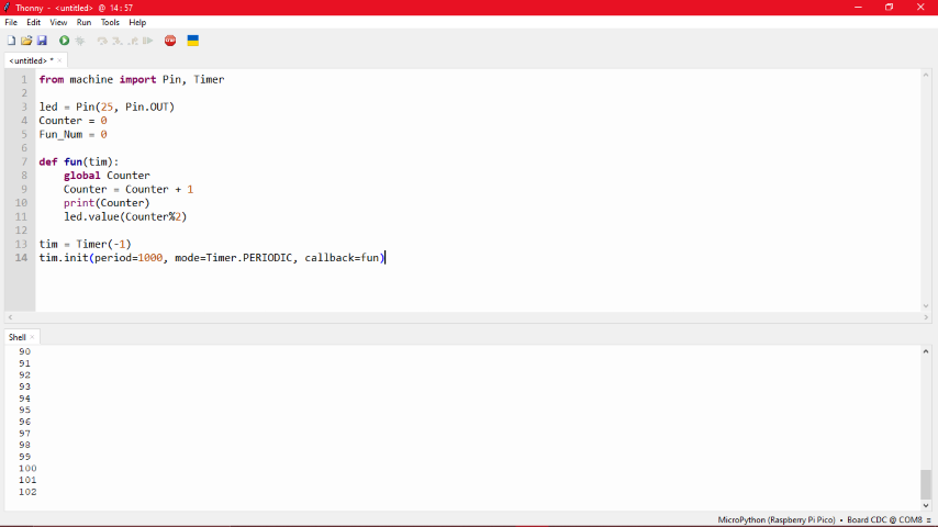
- Upload Code: Upload the code for lighting the built-in LED and this is the output received.
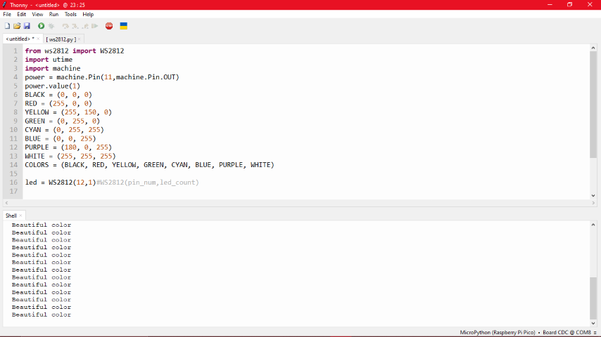
- Upload Code with library: To light up the RGB LED, we need a library that we will save onto Raspberry Pi Pico and then upload the code to get this output.
Other Architectures:
For this week’s group assignment at Fab Academy, we are collectively delving into the exploration of alternative architectures and their respective development workflows. To facilitate this exploration, we have obtained various development hardware boards from our lab’s inventory, with the assistance of our instructors to kickstart our journey.
The hardware boards we have acquired for experimentation include:
- Arduino Uno ATMEGA328P
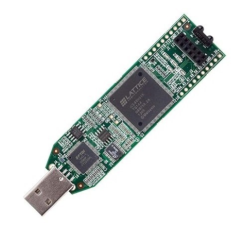
- Lattice ICEstick Evaluation Board (FPGA Development board)
Arduino Uno
ATMEGA328P
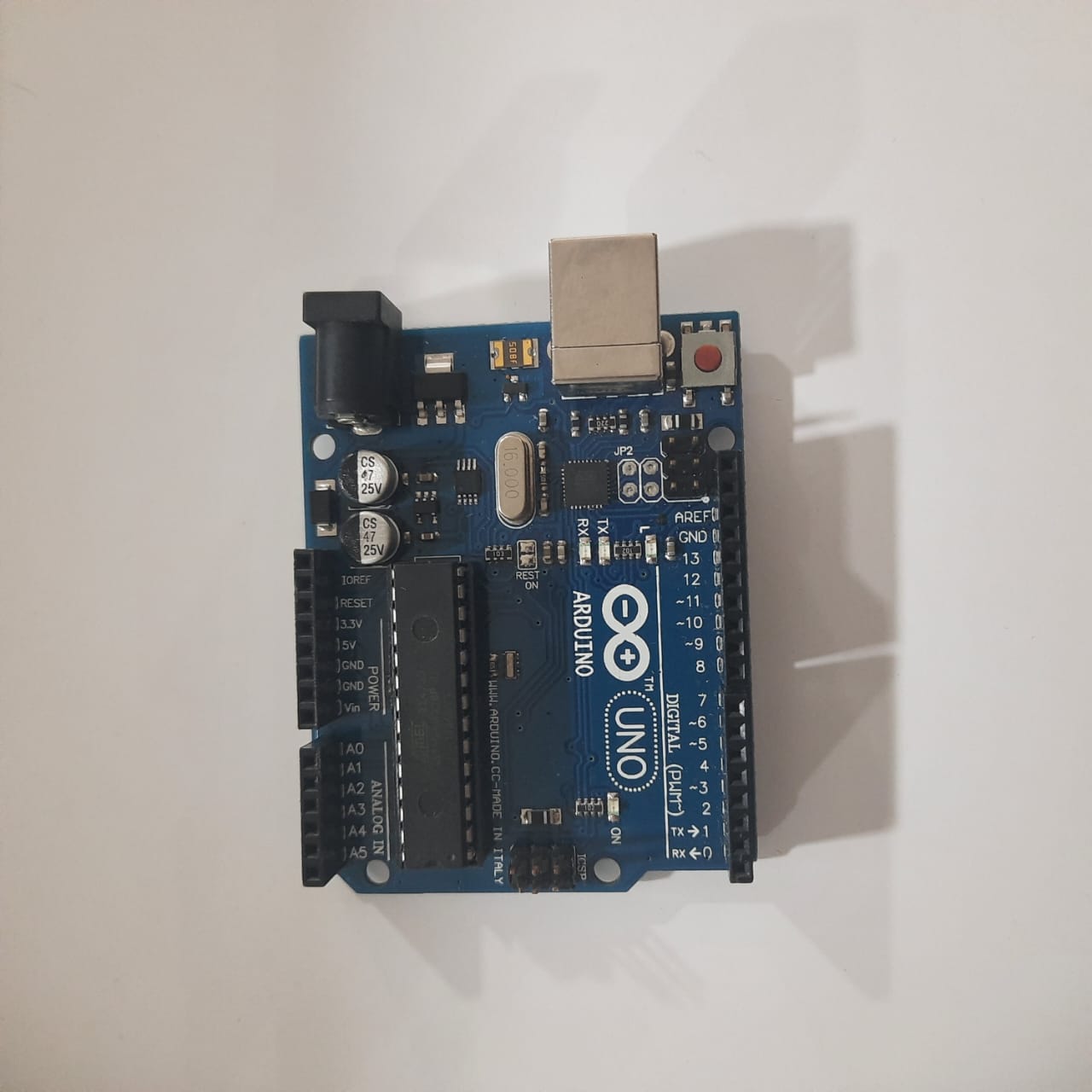
- Microcontroller: ATmega328P, an 8-bit AVR microcontroller.
- Digital I/O Pins: 14 (including 6 PWM outputs).
- Analog Inputs: 6 analog input pins.
- Communication Interfaces: 1 hardware UART, I2C, and SPI.
- Operating Voltage: 5 volts.
- Clock Speed: 16 MHz.
- Form Factor: Standard size.
- Compatibility: Programmable using the Arduino IDE. Compatible with various shields.
- Applications: Suitable for a wide range of projects, including prototyping, educational purposes, and hobbyist projects.
Workflow with Arduino IDE
To use the microcontroller with the Arduino IDE, you’ll need to follow these steps:
-
Install Arduino IDE: If you haven’t already, download and install the Arduino IDE from the official Arduino website.
-
Select Board: After installation, go to “Tools” > “Board” and select “Arduino Uno”
-
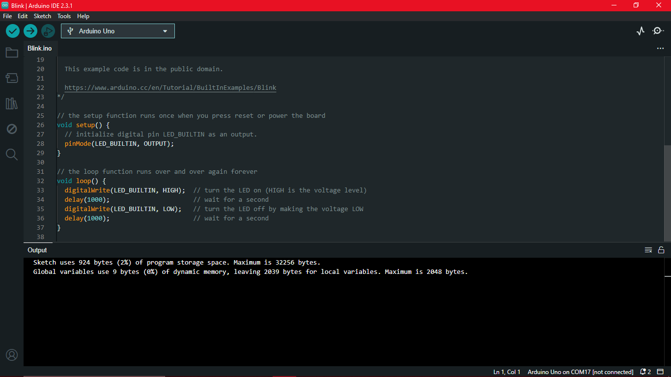
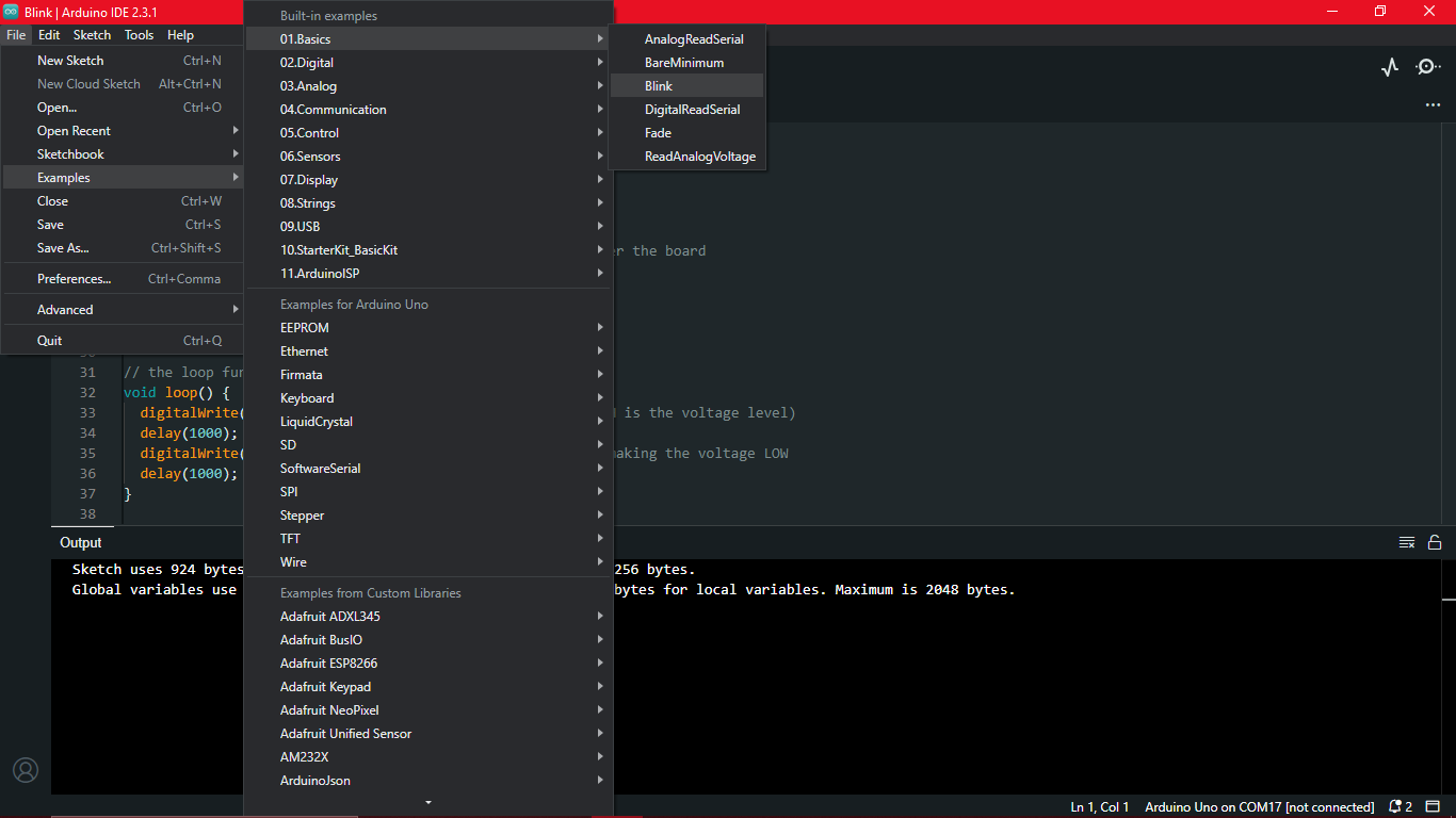
Write Code: First we tried, the Blink program from “Files”> “Examples” > “Blink”
-
Upload Your Sketch: Connect board to computer via USB. Ensure that the correct port is selected under “Tools” > “Port”. Then, click the “Upload” button to compile and upload sketch to the board.
-
Verify: Once uploaded, verify that sketch is running correctly on the board.
FPGA Development board
The Lattice ICEstick Evaluation Board
The Lattice ICEstick Evaluation Board is a development platform designed by Lattice Semiconductor specifically for prototyping and development with their iCE40 FPGA family. It’s a low-cost, easy-to-use platform that provides users with an accessible way to learn about and experiment with FPGA technology.
Key features of the ICEstick Evaluation Board include:
-
iCE40 FPGA: The board features a Lattice iCE40 FPGA, which offers low power consumption and high integration in a compact package. This FPGA family is known for its ease of use and flexibility, making it suitable for a wide range of applications.
-
USB Connectivity: The ICEstick Evaluation Board connects to a computer via USB, allowing for easy programming and communication with the FPGA.
-
Onboard Components: The board includes various onboard components such as LEDs, push buttons, and I/O headers, which can be used for testing and interfacing with external circuits.
-
Programming and Configuration: Users can program and configure the FPGA using Lattice’s design software tools, such as Lattice Diamond Programmer or Lattice Radiant, which provide a comprehensive environment for designing, simulating, and programming FPGA designs.
-
Educational and Hobbyist Use: The ICEstick Evaluation Board is often used in educational settings and by hobbyists to learn about FPGA technology, digital design, and embedded systems development.
Overall, the Lattice ICEstick Evaluation Board serves as an accessible and versatile platform for exploring FPGA technology and developing FPGA-based projects.
Workflow with IceStudio
To use IceStudio for FPGA development with the Lattice ICEstick Evaluation Board, you can follow these general steps:
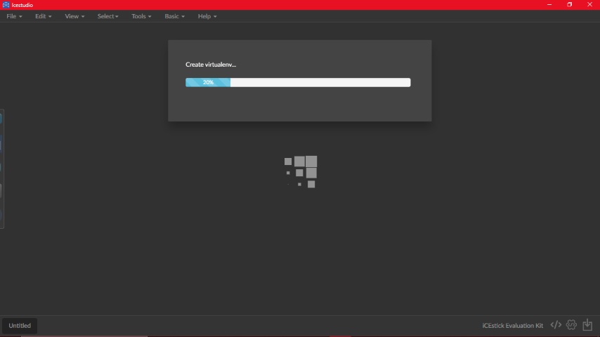
- Install IceStudio: Begin by installing IceStudio on your computer. IceStudio is a graphical FPGA development environment that simplifies the process of designing and programming FPGAs. You can download IceStudio from its official website and follow the installation instructions provided.
 https://downloads.icestudio.io/
 https://icestudio.readthedocs.io/en/latest/source/installation.html
-
Connect the ICEstick Board: Connect your ICEstick Evaluation Board to your computer via USB.
-
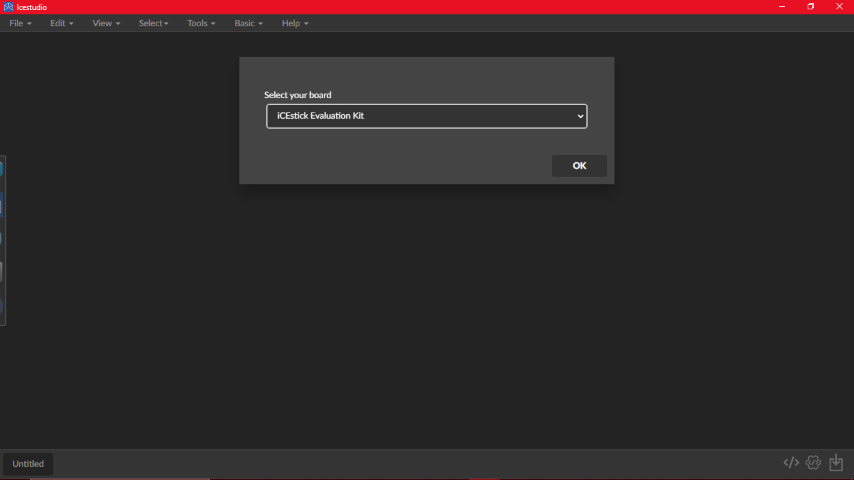
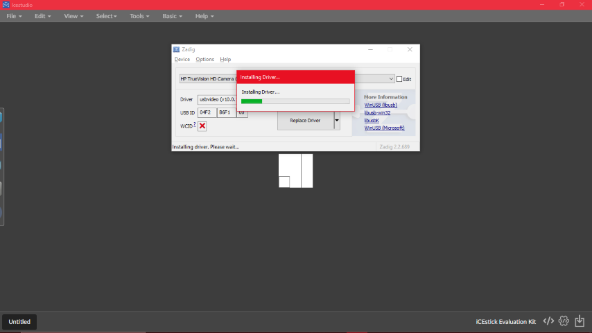
Launch IceStudio: Open IceStudio on your computer. Select the board and install the driver.
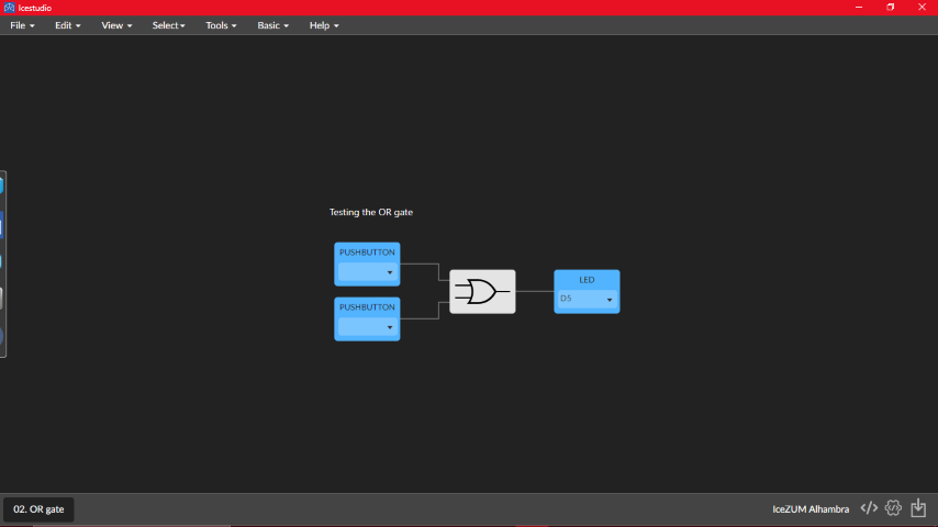
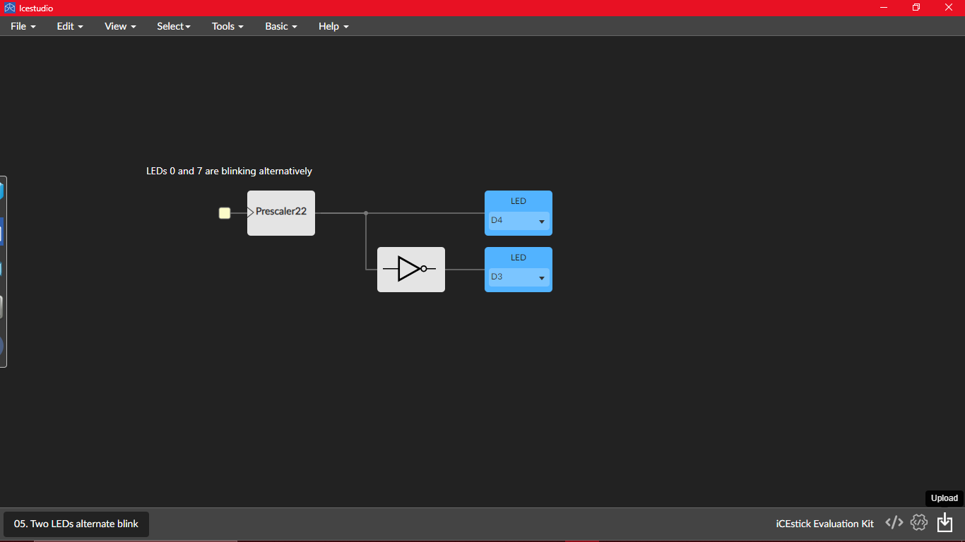
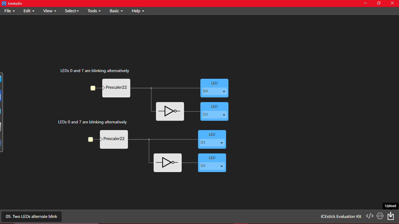
- Design FPGA Project: There are lot of options to explore and several examples to get started like this.
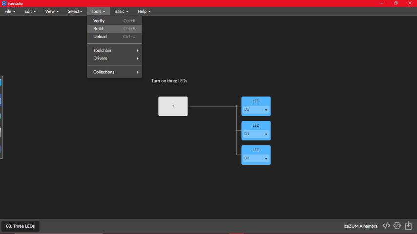
- Compile and Program the FPGA: Once we’ve designed your FPGA project in IceStudio, we can upload it onto our board using three steps. Verify. Build. Upload.
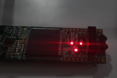
- Alternate Blink with 2 LED
- Alternate Blink with 3 LED
Performance
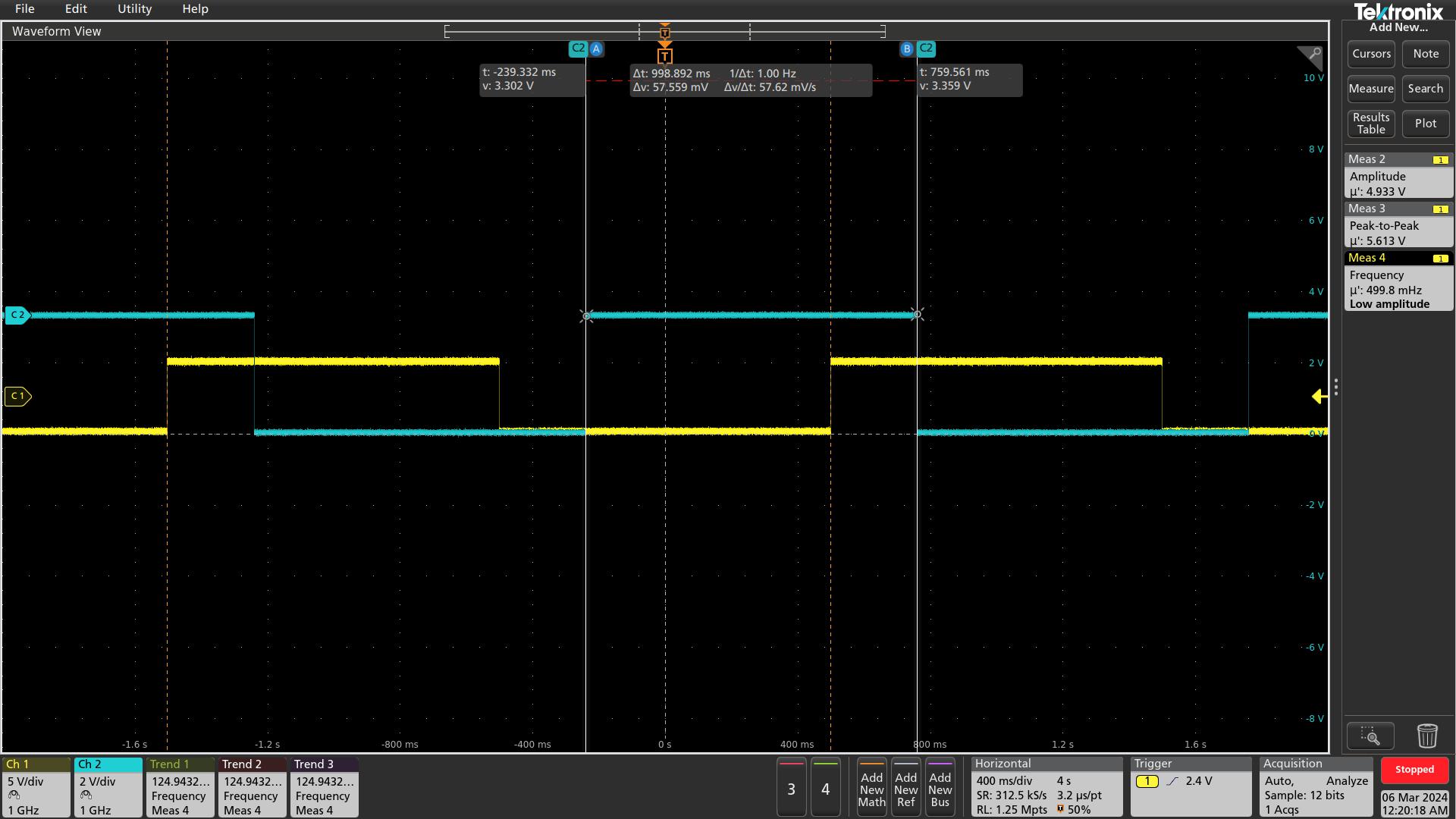
So now we will be comparing the performance for the two boards.
To compare the boards, we have uploaded the blinking of an LED to the three boards in different IDEs.
So first, we measured the performance of Seeed XIAO RP2040 in our DS0 and here is the graph we got:
t=998.892ms
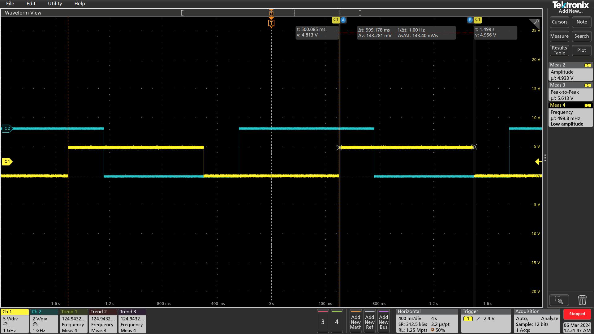
Next, we measured the performance of Arduino in our DS0 and here is the graph we got:
t=999.172ms
Comparison