Week 8: electronic designing☀
This week is going to be one of the more scary weeks. This is the week in which we will be making the very first version of my final project board! To get to the point this week is about elctronice designing. We would have to design our final project board and print it. This week is going to be really fun so lets get right into it!😀
Neil's lecture😋
After the random reviews were finished, we started with our lesson for the week. It was really fun while professor Neil talk about all that is needed for elctronic designing. He also talk on different editing softwares that we could use to design our boards.
Assignments
✓ Try designing a final project board and mill it.
✓ Scolder the components onto your boards
✓ Test and try programming your board
This is going to be a tiring week! We have to create a board and mind I say creating a circuit board is one of the most stressfull things that I have ever done!!!
Group Assignment
Here is the group assignment of the week! --> Here
For this weeks group assignment, we had to to use tools to observe the signals from a micro controller
We for the group assignment, we used multimeter and then the oscilloscopes to measure the signals of a micro controller and then used the oscilloscopes to visually witness the signals respectively.
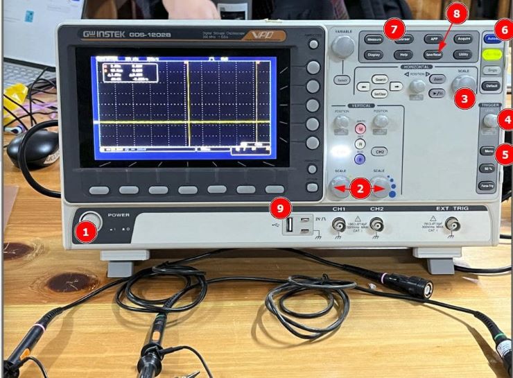
Details
- Power Button: Turns the oscilloscope on/off.
- Vertical Scale Knobs: Adjusts the vertical scale (volts per division) of the waveform.
- Horizontal Scale Knobs: Adjusts the horizontal scale (time per division) of the waveform
- Trigger Level Knob: Sets the trigger level for synchronization.
- Trigger Source Button: Selects the input channel for triggering.
- Auto Setup Button: Automatically adjusts the oscilloscope settings for optimal waveform display.
- Cursor Measurement Buttons: Enables measurement of various parameters such as voltage, time, frequency, etc., using on-screen cursors.
- Save/Recall Buttons: Allows saving and recalling of waveform settings and data.
- USB Port: Facilitates data transfer and storage via USB connection.

A multimeter is a handheld device that combines several measurement functions into a single unit. A multimeter usually consists of a digital or analog display, a selection knob, and input slots for connection probes. Multimeters can measure DC and AC voltage, DC and AC current, resistance, continuity, capacitance, frequency, and sometimes even temperature 🔥.
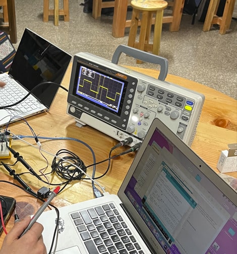
This is us using the oscilloscope to measure the pwm values form the a micro controller board.
Reflection of this group assignment
This week we could see into what actually happens while a micro controller does it tasks. How it send signals and then also I got a better understanding of how electronics work! I got to work with the oscilloscope and it was so cool handling it! It was a bit nerving the first time I tried using the oscilloscope but after a while I got used to using it. I learned a lot and also found a new way to debug.
During the Week of Electronics Design in the Fab Academy program, the group assignment focuses on utilizing the skills and knowledge acquired in electronics design to collaboratively create functional circuit boards. Students are tasked with working together to design and fabricate their final project circuits or systems. Through the use of tools like multimeters and oscilloscopes, the group is required to thoroughly check their circuit boards for proper functionality.
Electronic designs🧐!
Now lets get into this weeks assignments and start this week up! To begin lets start off with designing our final project board in a schmatic editor😤.
The editor that I will be using is Kicad .
KiCad is an open-source Electronic Design Automation (EDA) suite that provides tools for schematic capture, PCB layout, circuit simulation, 3D rendering, and more. It is widely used by hobbyists, students, and professionals for designing electronic circuits and printed circuit boards.
Kicad Provides a lot different features that is really useful for electronic designing. But the main features I will be using is the schematic editor(To create circuits) and PCB editor (To design printed circuit boards)
This is a simple tutorial to install kicad on your device.
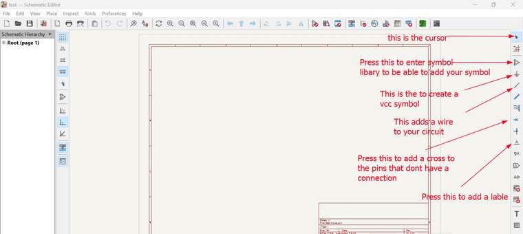
Now Lets start with the creation of our circuit with the schmatic editor! Though before we start using it we have to install the fab libary of both footprints and symbols. Lets get right into😜.
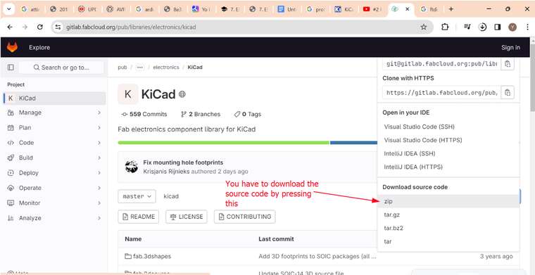
Firstly we have to install the fab libary. This is the documentation through which I was able to install the fab libary -->Here
I first had to download the source code of the git repository. After that I extrated it somewhere save for me to access it later.
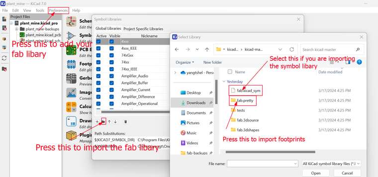
I now have to open up the symbol libary and the footprint libary in Kicad and then go to preferences and go to either Manage symbol or Manage footprints. After that you press the symbol that looks like a file and upload the file that you downlaoded.
After that you can just open up your schmatic designing and enjoy your full fab libary☕.
Designing🤠!
Now lets get into designing our final project board! Though lets first get into all the different features that kicad has to offer!
This is the tutorial through which I learned how to design in the kiacd schematic design.
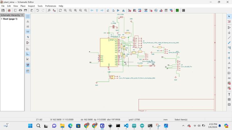
Now lets get into all the components that I need to create the my final project board😀! The components I added to my skematic for my circuit board were.
✓ a conn 01x06 pin
✓ a conn 01x04 pin
✓ a conn 01x03 pin
✓ a power led
✓ a programmable led
✓ some extra 0 ohm resistors.
Wow, that was a lot of extras 🥲. Still then each and every one of the extra components added are to do a specific task. Both the power and programmable led are for assurance for whether the board works or not. While the pin are mainly to control sensors! I made this board with my final project in mind, cause of that each of the conn pin header is relative to a sensor from my final project.
1x6 pin header - This is for the NPK sensor which requires 6! pins, (Thats a lot 🤯)
1x4 pin header - This is component is for the I2C LCD which has four pins.(Thats a bit easier🥲)
1x3 pin header - Lastly this is for the comparative soil moisture sensor(This is the easiest😋)
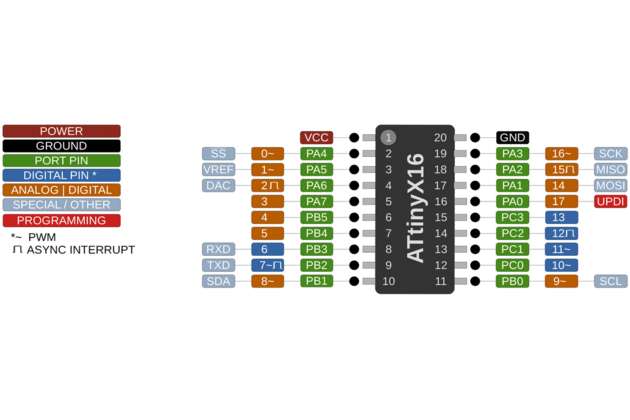
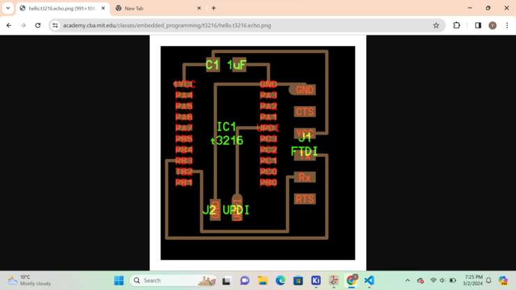
Ahh... almost frogot, the micro controller that I used for this week was the attiny 3216 micro controller. I used the fab academy; embedded programming page to find my self a bit of an idea on how the board should come out.
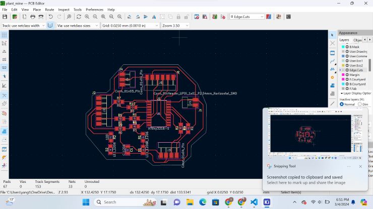
This is how my finished schmatic looks like.
Now lets start with the PCB editor!
PCB creation 💀
(Ohh lord, please have mercy on my soul).
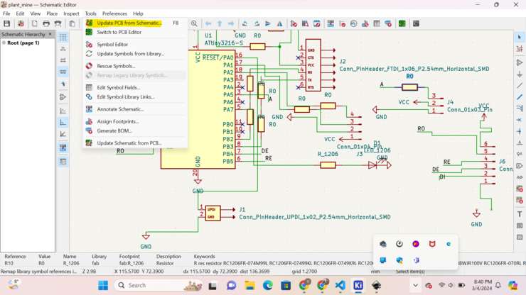
So before we get into editing our PCB, We have to convert our schematic design to our PCB editor. To do that we have to go to "tools" and then "Update PCB editor form schematic".
Now lets begin!!!
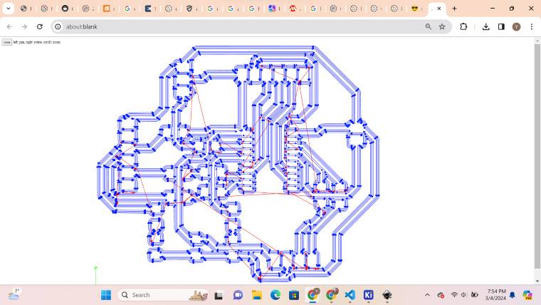
This is my very first attempt, and.... it did not work out the way i envisioned.
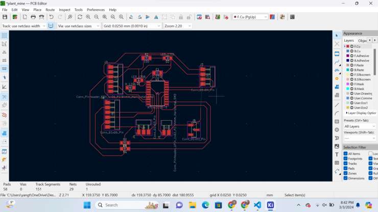
Ohh... When I realised I couldn't, in any way get the last wire out of its place. My heart just sunk and it felt as if I had aged a thousand years!😭.
I had to get this done so I didnt give and continued onwards! After what seemed like an eternity, I finally finished with the PCB editing. Thank lord!!
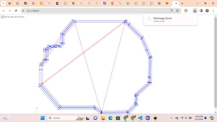
Converting to RML file!
With the hardships behind us, lets get into creating the RML file. This how the code looks!
This is how the RML file looks for both the edge and the traces
Traces
Interior
 .
.
Milling😰
OHH... Great Buddha, Great God and Great Monks. Please have mercy on this little boys soul as he ventures far beyound his comfort zone!
This is always the scary part for anyone creating a PCB. The countless ways in which things could get messed up and you ending up with a broken mill bit!
With all the necessary steps taken into place and more a half of my life wasted on this. This is how the milling went.
After close inspection of the board I noticed that the milling machine didnt cut the board properly as not all of the copper plate was milled by the machine. I almost fainted when I noticed that and was scared for my life😰!!
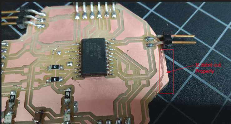
Later when my instructor,Anith Sir arrived. He suspected that the copper plate and the scarificial bed werent stuck properly which cause the problem. Additionally he also mentioned that the board might still work as the point of the board that didnt cut properly wasn't colliding and interupting with the rest of the board. Sir suggested that I would have to make sure that isn't interupting with the rest of the design by the use of the multimeter💀!
using the multimeter, I set it measure continuity. What this mode of the multimeter it checks wether the to points you connect to the to wires of the multimeter are connected or not. With the mode set I connect the to point of the micro controller. I connected one point to the mis-connected ground and then connected the other to all points of my board.
After a scary process of checking using the multimeter, IT WORKED!
Programming😃!
Now lets get into the world of programming! I wont be programming anything too complex. I just want to add the blink code so that to if my board is functional or not. Before I begin with the programming, I have to follow the necessary step to be able to program my board.
Firstly I have to install the arduino ide through which I will be programming my board. To install arduino IDE go to this link right here --> Here
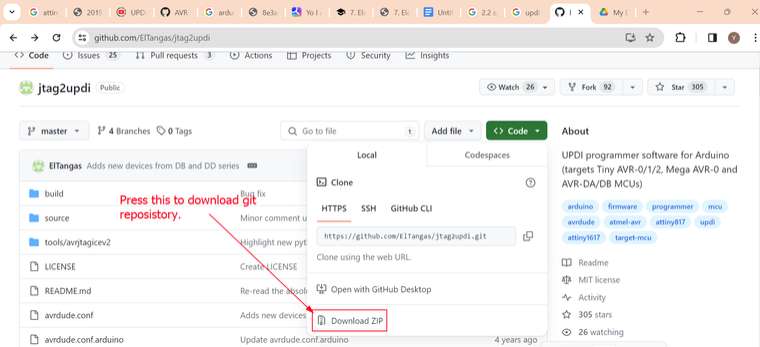
Now to program my attiny 3216 micro controller I have to use a updi (Unified Programming and Debugging Interface) prgrammer. To make the programmer I used the documentation by the user name of ElTangas. This documnetation included the program code to turn an arduino uno board into an updi programmer and all the steps needed to take to turn an arduino into an updi programmer!
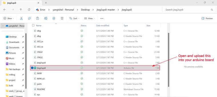
Firstly I had to install the git repository of ElTangas and then after installing the repo, inside the source folder there is an empty arduino ide file which you have to open and upload into your arduino. This will turn your arduino board into an updi programmer🥰!
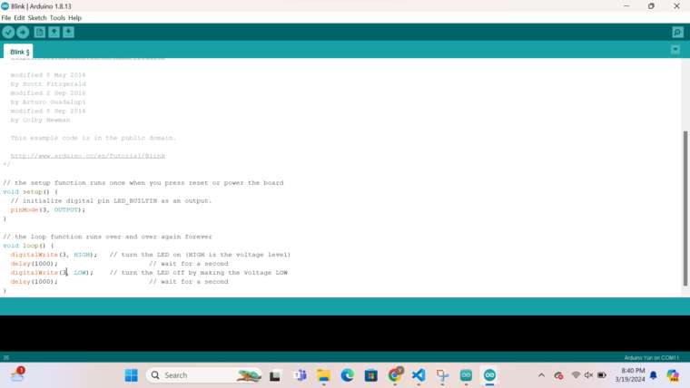
Now with the programmer being made, all I had to do was go to the example file and select the blink code. Then I changed the pins to match the pins for my board. (My LED pin is the 3rd pin.)
But there is one last step before you are able to upload your code. You now have to select the correct board for programming. The board I chose is the attiny 3216. To get my board I first inserted the libary url to my perferences.
[http://drazzy.com/package_drazzy.com_index.json]
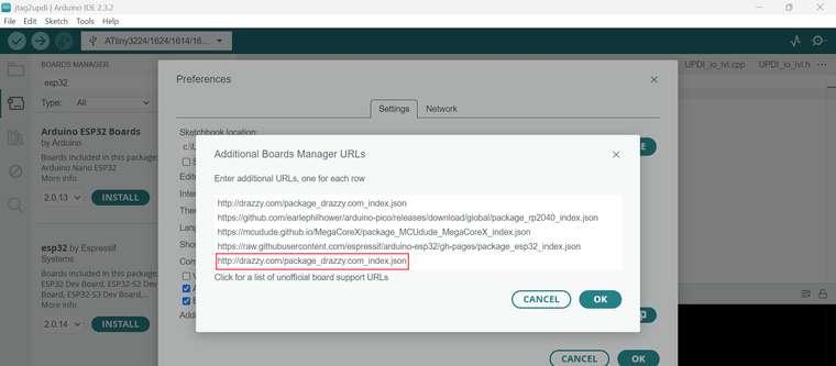
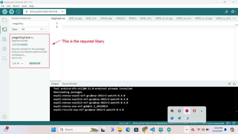
After that I had to go to board manager and then I had to install the megatiny core board libary.
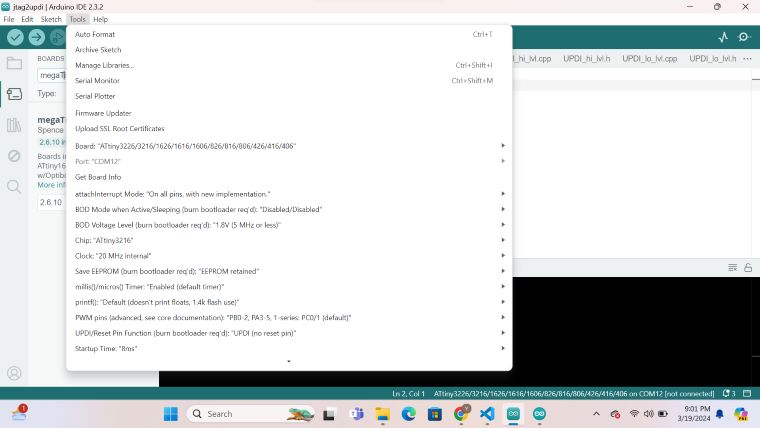
Then after that I had to select the correct tools such as the boards, chip and programmer.
Now you can finally start uploading and programming your board.
This is the code I used in the above video
  // the setup function runs once when you press reset or power the board
  void setup() {
    // initialize digital pin LED_BUILTIN as an output.
    pinMode(3, OUTPUT);
  }

  // the loop function runs over and over again forever
  void loop() {
    digitalWrite(3, HIGH);   // turn the LED on (HIGH is the voltage level)
    delay(1000);                       // wait for a second
    digitalWrite(3, LOW);    // turn the LED off by making the voltage LOW
    delay(1000);                       // wait for a second
  }