Week 8: Electronics Design

Assignment of the week:

Group assignment:

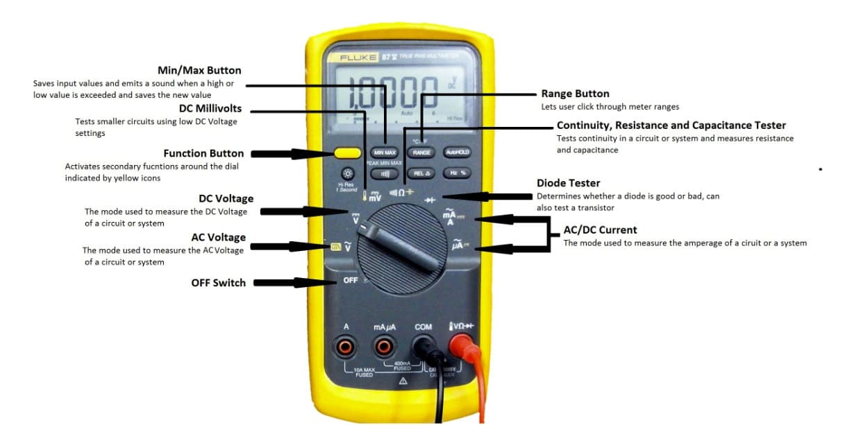
Use the test equipment in your lab to observe the operation of a microcontroller circuit board (as a minimum, you should demonstrate the use of a multimeter and oscilloscope)

Document your work on the group work page and reflect what you learned on your individual page

Individual assignments

Use an EDA tool to design a development board to interact and communicate with an embedded microcontroller

Learning outcomes:

Select and use software for circuit board design

Demonstrate workflows used in circuit board design

Requirements for the documentation:

Linked to the group assignment page

Documented what you have learned in electronics design

Checked your board can be fabricated

Explained problems and how you fixed them.

Included original design files (Eagle, KiCad, etc.)

Included a ‘hero shot’

Here comes another schedule for another week!!

alt text

Group Assignment

Summary of the group assignment

Oscilloscopes and Multimeters:

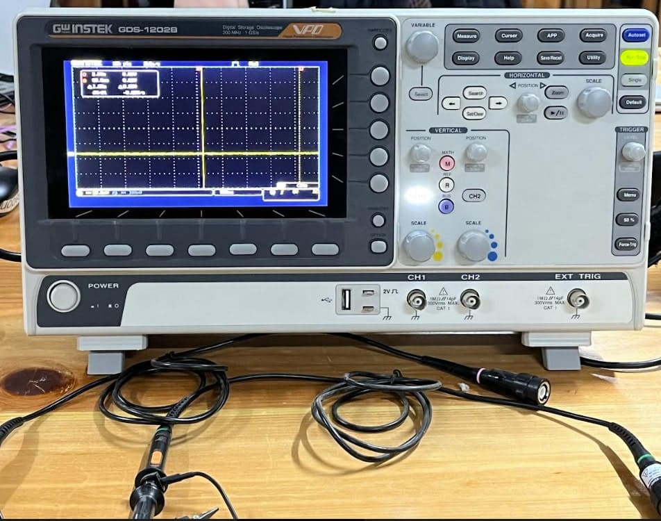
This week, we learned about oscilloscopes, which are tools used in electronics to see voltage changes over time. They work by converting electrical signals into visible waveforms on a screen. We explored the functions of a specific oscilloscope model and connected it to a microcontroller board to understand circuit behaviors better.

Additionally, we discussed multimeters, which measure voltage, current, resistance, and continuity in circuits. They work by applying known values and using Ohm's Law for calculations. We looked at the buttons and functions of a typical multimeter and learned how to connect it properly to circuits for accurate measurements.

Image Source.

Overall, the hands-on experience with these tools helped us understand circuit concepts better, refine troubleshooting skills, and improve collaboration and communication within our group.

Here is the complete group assignment.

KiCad

During our pre-fab time, our local instructor taught us to use KiCad. He introduced us to the basic tools and techniques for creating schematics and PCB, therefore I am more comfortable using this software than the other softwares.

KiCad is an open-source tool for designing electronic circuits and Printed Circuit Boards (PCBs). It allows users to create electrical schematics and seamlessly transition to designing the physical layout of PCBs, ensuring accurate component placement and trace routing.

Getting started with KiCad:

Step 1: Install KiCad

I downloaded and installed the latest KiCad version from the official KiCad website.

Step 2: Open KiCad

Then I launched KiCad after a successful installation.

Step 3: Create a New Project

  1. Select "File" -> "New Project" -> "New Project."

  2. Set the project name and location.

Adding libraries in KiCad

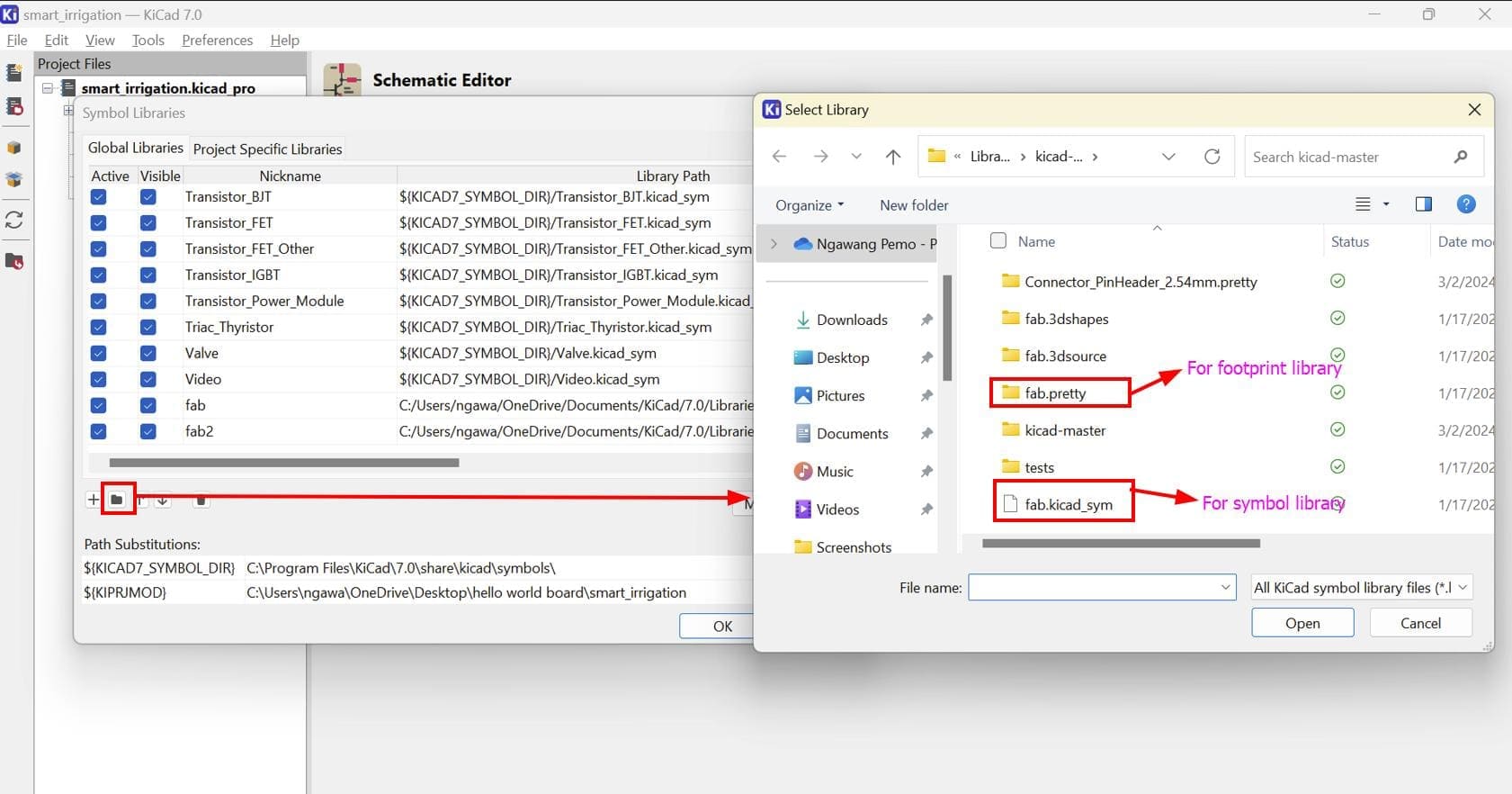
To add libraries in KiCad, first download your desired library. For my board I downloaded the library from here.

Then in the project window tap on preferences and choose either symbol library for components and footprint library for components' footprint.

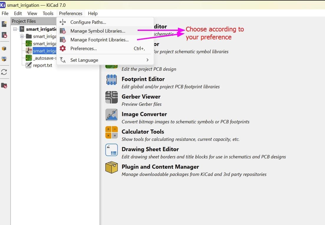
After that a square will pop up where you can select the folder icon and add the downloaded library.

Creating schematic design:

In the project window:

  1. Right-click on the project name.
  2. Select "Add New" -> "Schematic."

There are many features of KiCad which we use to create a schematic design. To know each of their functionalities, we can move our cursor on the components and wait till their functions show up.

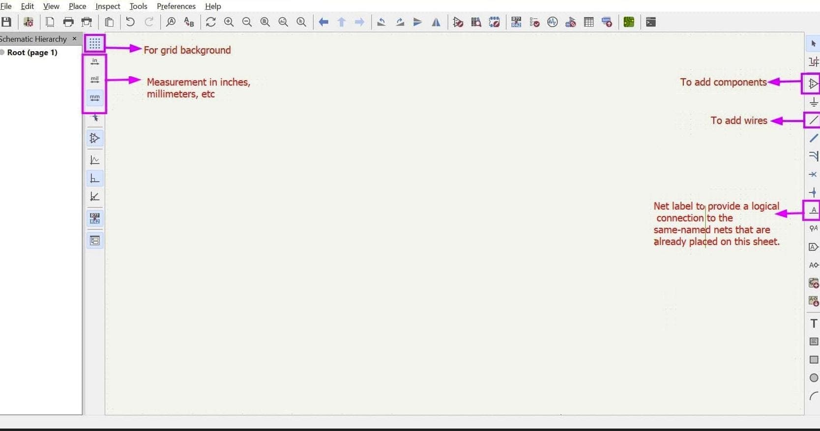
Here are some basic tools you have to use for a schematic circuit:

ATtinyX14

So, for this week, I am planning to program the ATtiny1614. Here is the pinout of the mcu.

Image Source.

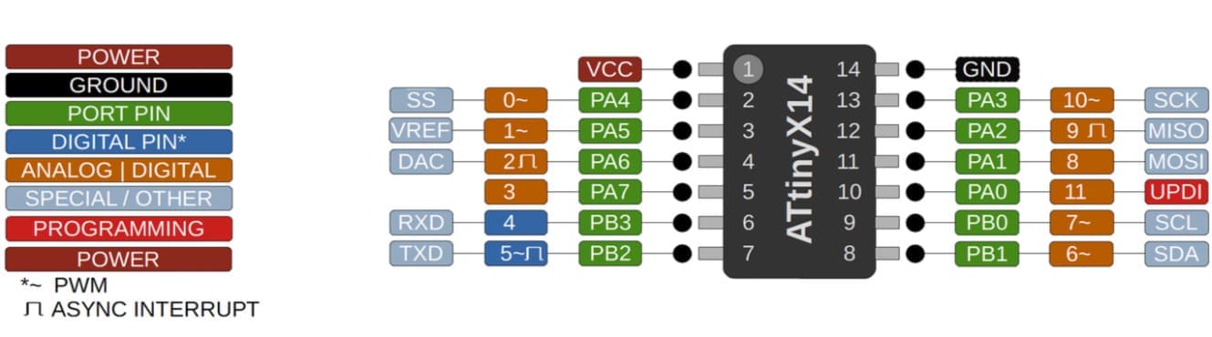
Then I went to the Fab Academy embedded programming site and found the ATtiny1614 board connection. .

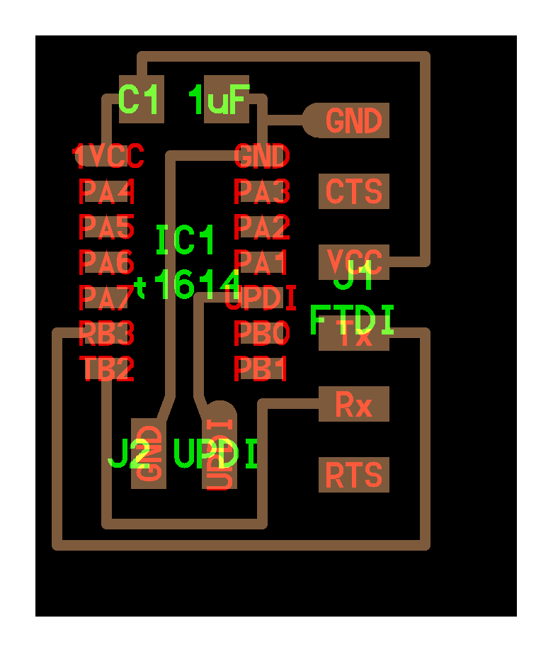
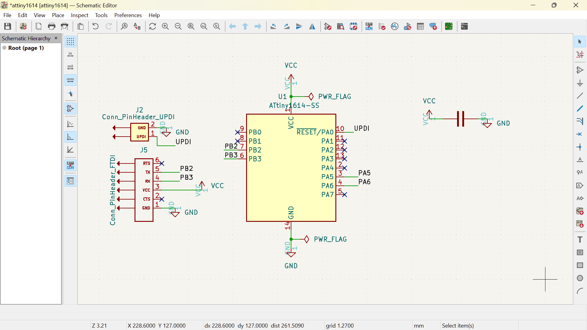
For my own board, I added a power LED, a programmable LED, a switch, and resistors.

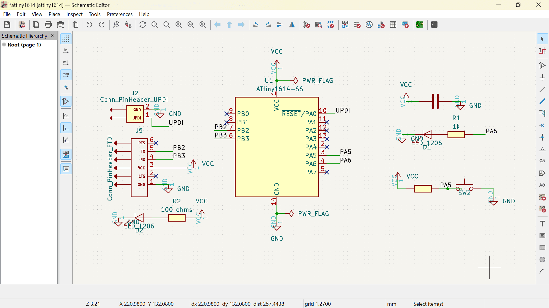
I added labels to make the circuit easy to interpret and to keep it clean.
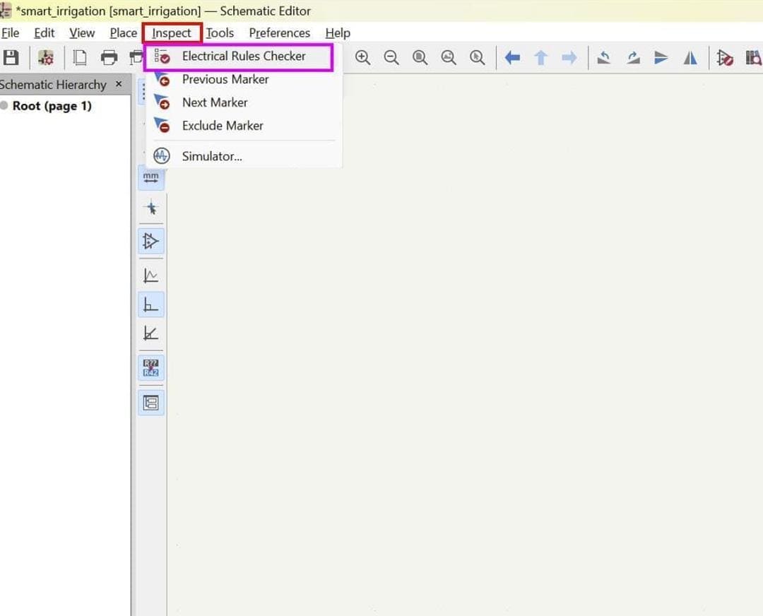
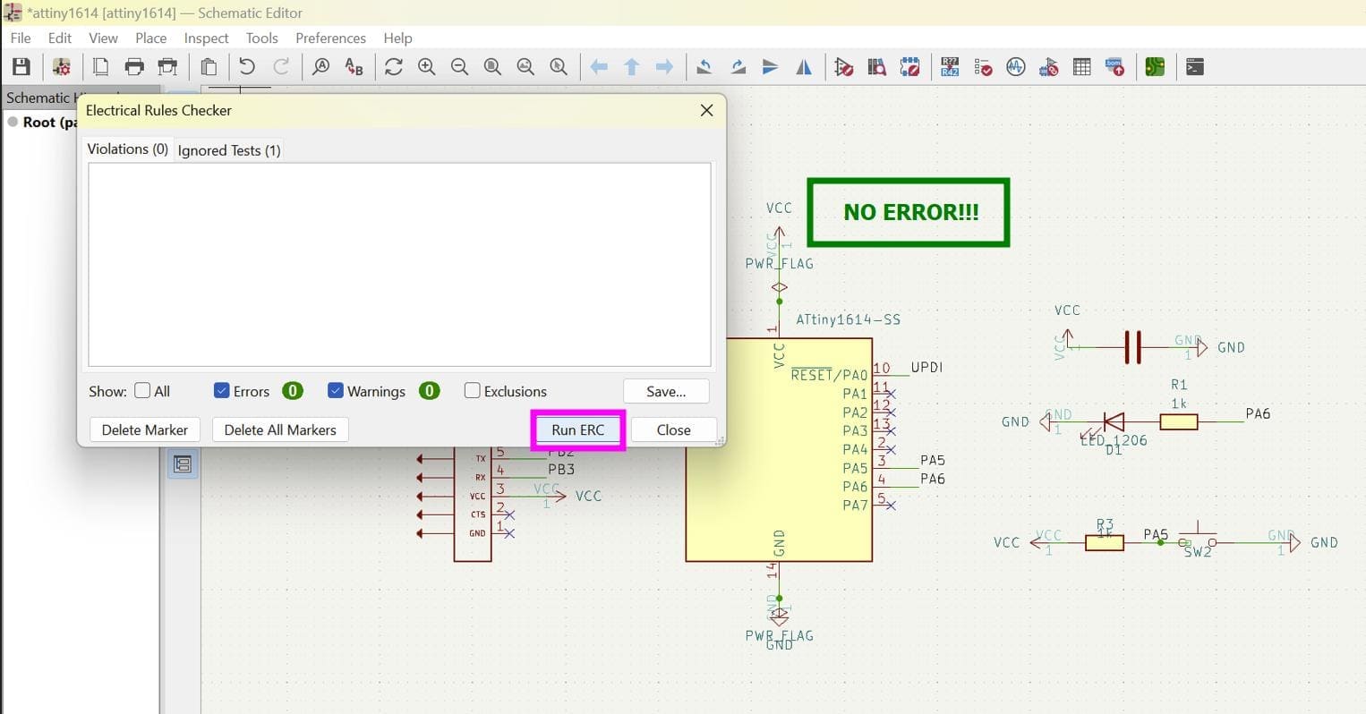
Run ERC

While designing your schematic board, don't forget to run the electrical rules checker to find errors or incomplete connections in your design.

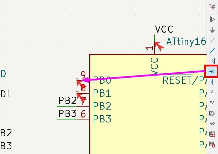
If some of the pins are not connected anywhere, attach no-connection flags to those to avoid errors while running the erc.

After running the ERC, NO ERROR!!

Here is the final look of my schematic circuit:

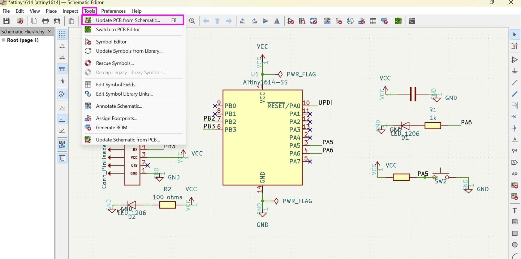
Now to update the schematic to PCB format, first click on tools and then select update PBC from schematic option.

PCB Design

To start with the PCB designing, we have to first specify the Design Rules and Constraints. Let's do this:

Design Rules and Constraints

In PCB design, it is crucial to begin by specifying the "Design Rules & Constraints." These rules ensure that the PCB can be manufactured and functions as intended. One key aspect is the definition of net classes, but this is just a part of the overall process. Here are some critical points to consider:

1. Minimum Distance Between Trace Lines

The minimum distance between trace lines is determined by the capabilities of the manufacturing process, specifically the diameter of the endmills used. Smaller endmills allow for tighter spacing, but it's essential to set this minimum distance correctly to avoid short circuits and ensure signal integrity.

2. Minimum Gap Between Pads

Similarly, the gap between pads must be set based on the endmill size. This ensures there is enough clearance to avoid solder bridging during the assembly process. Proper gap settings are critical to prevent manufacturing defects.

3. Design for Manufacturability (DFM) Rules

These rules encompass various aspects such as:

4. Electrical Constraints

These constraints ensure that the board meets the electrical performance requirements:

5. 3D Design Rules and Constraints

With modern PCB design tools, 3D checking capabilities allow designers to visualize and verify the board layout against mechanical constraints and other system components. This includes:

6. Setting Up Rules in CAD Systems

Using tools like Cadence Allegro PCB Editor’s Constraint Manager, designers can set up and manage these rules effectively. This includes:

Summary

Setting up comprehensive design rules and constraints is essential for successful PCB layout and manufacturing. These rules need to be defined and tailored to the specific manufacturing capabilities and electrical requirements of the design. This process begins in the schematic phase and continues through the layout, ensuring that all aspects of the PCB design are accounted for and that potential issues are identified and resolved early in the design process.

Here's my settings:

More to note:

While creating routes, we should also keep in mind to avoid right angle connections because according to Altium, "high-frequency signals emit Radio Frequency radiation at every 90 degree turn of the copper track." (Altium, 2018, para.3)

Mr. Rico suggested us to keep the width of the signal pin routes 0.4 mm and power pin routes 0.8 mm so that the power can flow smoothly and to help us differentiate the signal and power routes.

To adjust the routes, I went to Track: use netclass width > Edit Pre-defined Sizes and here are the sizes that I added

These are the basic tools that I used for the PCB designing!

Run DRC

Like you ran ERC for schematic, it is also important for us to run the design rules checker for PCB design to ensure there is no design error in your board and guide you to improvise your board.

Here is the final look of my PCB design

And here is the printed board!!!

Time to solder!

These are the components :)

After soldering!!!

Programming microcontroller development board:

To program the board, I first downloaded the jtag2updi from this link This is a firmware designed for ATmega328P and similar AVR microcontrollers. It allows these microcontrollers to communicate with avrdude using the jtagice Mk2 protocol over a serial link.

Purpose of jtag2updi:

- It enables an ATmega328P or similar AVR MCU to interface with avrdude using the jtagice Mk2 protocol via a serial link. - Specifically useful for programming the attiny817 family of MCUs that use the UPDI interface. After extracting the file, I went to the source folder and opened the `ino` file.

After opening the file, a folder named `jtag2updi` appeared. Then I copied all the files included in `source` and pasted them in in the new folder.

Now when I open the jtagupdi ino file, it appears like this:

To program the ATtiny1614 I followed this tutorial and I also referred to Adrian's Documentation

After I made all the connections, I connected my board to the breadboard and the Arduino to my laptop with USB 2.0 Cable Type A/B.

Now, open your Arduino IDE and go to files > preferences. Then paste the link in the Additional Boards Manager Urls

Now, go to tools > board > boards manager

Search for megaTinyCore and install the file

After the installation, go to tools > board > megaTinyCore > select the section which has the ATtiny1614

Now, hover your cursor to chip and specify it as ATtiny 1614

I am programming my board with Arduino, so I have to select the `jtag2_updi option` as the programmer

Here is the picture of the labelled connection I made for the board.

Lastly, I uploaded the blink program after setting the pin number to 2 and the LED blinked!!!

Communication

For the communication part of the assignment I will try to send data through my board saying "button pressed," when the button on my board is pressed.

SoftwareSerial Library

For this assignment I will need to use the SoftwareSerial Library because the SoftwareSerial library allows serial communication on other digital pins of an Arduino board, using software to replicate the functionality (hence the name "SoftwareSerial"). It is possible to have multiple software serial ports with speeds up to 115200 bps. A parameter enables inverted signaling for devices which require that protocol.

Here is the code I used for the communication:

Highlighted Code
    #include 

        const int buttonPin = 1;
        const int ledPin = 2;
        
        SoftwareSerial mySerial(4, 5); // RX, TX
        
        void setup() {
        
          pinMode(buttonPin, INPUT);
          pinMode(ledPin, OUTPUT);
        
          Serial.begin(9600);
          mySerial.begin(9600);
        
          digitalWrite(ledPin, LOW);
        }
        
        void loop() {
          
          if (digitalRead(buttonPin) == HIGH) {
            
            digitalWrite(ledPin, HIGH);
        
            mySerial.println("Button pressed!");
        
            delay(100);
          } else {
            digitalWrite(ledPin, LOW);
          }
        }


Note: Don't forget to define the TX and RX pins as we will be using the ftdi cable for the communication.

I first uploaded the above code using the jtagupdi and then connected the ftdi cable for the communication part.

Here is the video!

Zipped Code files:

Blink LED Code

Communication Code

Thank You Message

Thank you for visiting!!!