Group Assignment:
Group Assignment Link:
____________
Oscilloscope Tool
(As Described by ChatGPT v.4o, 18th June, 2024)
An oscilloscope is a crucial electronic test instrument that provides a visual representation of electrical signals. It primarily plots voltage against time on a graph displayed on its screen, where the horizontal axis (X-axis) represents time and the vertical axis (Y-axis) represents voltage. This allows users to observe and analyze the waveform of the signal in real-time.Key functions and uses of an oscilloscope include:
1. Visualizing Waveforms: It helps in displaying the shape of electrical signals, which can be periodic, transient, or static. This is vital for understanding the behavior of the signal over time.
2. Measuring Signal Parameters: Oscilloscopes measure various properties of the signal such as amplitude (peak voltage), frequency, period, rise time, and fall time. These measurements are essential for designing and troubleshooting electronic circuits.
3. Diagnosing Circuit Issues: By comparing the actual signal with the expected waveform, engineers can identify and diagnose issues like noise, distortion, or unexpected fluctuations in electronic circuits.
4. Capturing Transient Events: Oscilloscopes can capture and display transient events, which are short-duration signals or anomalies that are often difficult to detect with other instruments.
5. Phase Comparison: By using multiple channels, oscilloscopes can compare the phase relationship between two or more signals. This is useful in applications like signal synchronization and timing analysis.
6. Triggering: Oscilloscopes have triggering capabilities that allow them to stabilize repetitive waveforms and capture specific events of interest. This feature ensures that the waveform is displayed consistently and can be analyzed accurately.
Overall, oscilloscopes are indispensable tools in various fields such as electronics, telecommunications, medical device manufacturing, automotive testing, and physics research, providing deep insights into the behavior and characteristics of electrical signals.
Oscilloscope Wavelength Signal Results:
Using Channel 1 on the Handheld Multicomp Oscilloscope, and set to DC Coupling Mode, I was able to examine the Wavelengths of a Servo Motor and Hall Effect Sensor while they were Inactive & Active.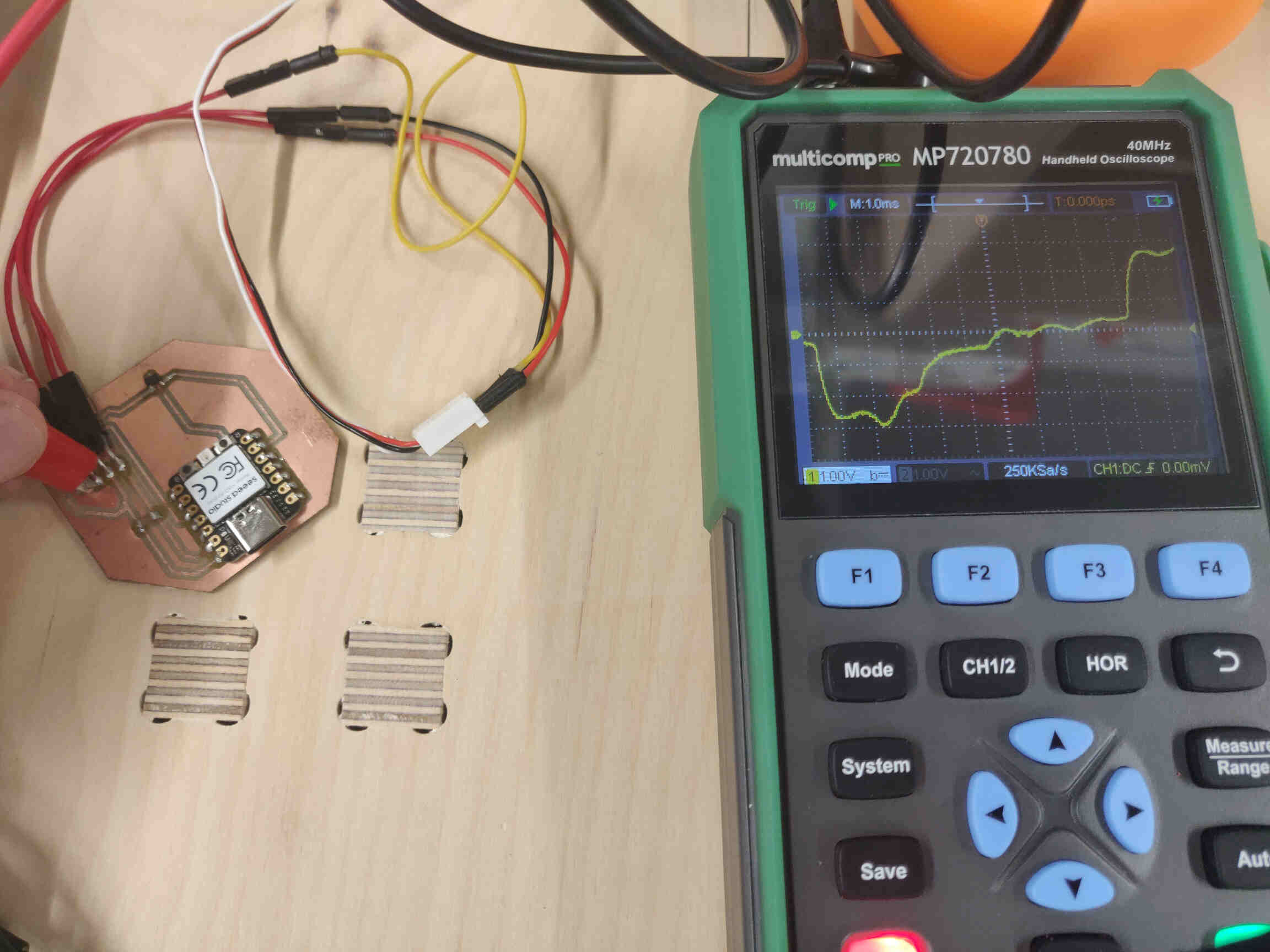
Oscilloscope: Servo Connection while inactive:
Wavelength stabilised at Verticle Scale 1.00Volts, Vertical Position 0.00div
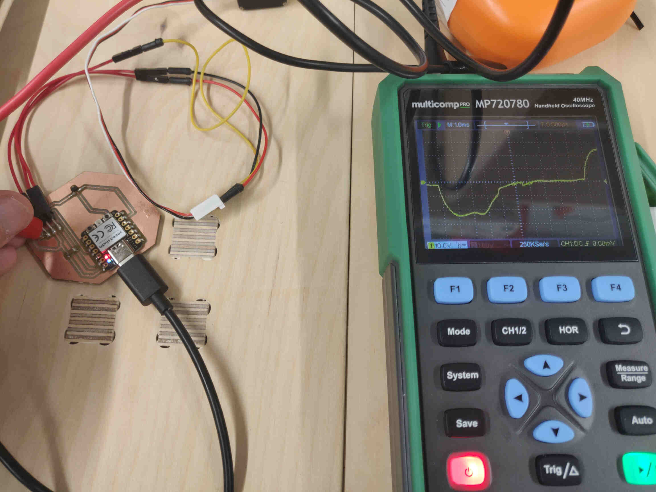
Oscilloscope: Servo Connection while active:
Wavelength stabilised at Verticle Scale 10.0volts, Vertical Position 0.00div
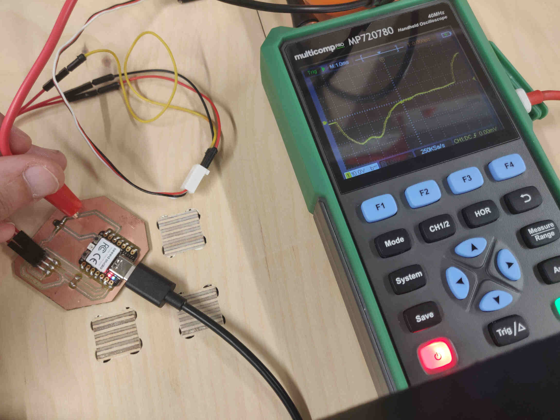
Oscilloscope: Hall Effect Signal Connection while inactive:
Wavelength stabilised at Verticle Scale 1.00Volts, Vertical Position 0.00div
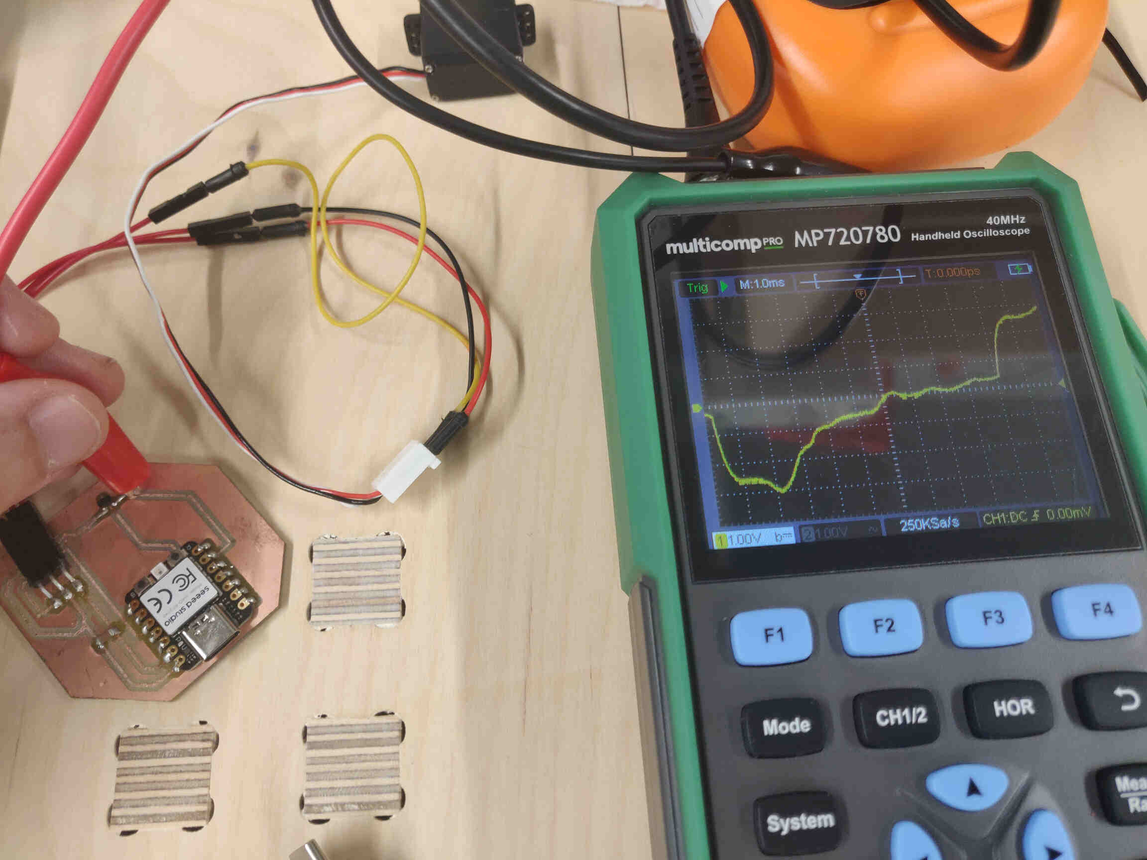
Oscilloscope: Hall Effect Signal Connection while active:
Wavelength stabilised at Verticle Scale 10.0volts, Vertical Position 0.00div
Multicomp Pro Guide by Element14
____________
Multimeter Tool
(As Described by ChatGPT v.4o, 18th June, 2024)
A multimeter is a versatile and essential electronic measuring instrument used to diagnose and troubleshoot electrical circuits. It can measure several electrical properties, most commonly voltage, current, and resistance. Multimeters come in two main types: analog, which uses a moving needle to display readings, and digital, which shows readings on an LCD or LED screen.Key functions and uses of a multimeter include:
1. Measuring Voltage: A multimeter can measure both direct current (DC) and alternating current (AC) voltages. This function is crucial for checking the voltage levels across components and ensuring they are operating within specified ranges.
2. Measuring Current: It can measure the flow of electric current through a circuit, either in DC or AC. This helps in determining whether the circuit is drawing the appropriate amount of current and diagnosing issues like overcurrent or short circuits.
3. Measuring Resistance: A multimeter measures the resistance of electrical components and circuits. This is useful for checking the continuity of wires and connections, as well as identifying faults in resistive components.
4. Testing Continuity: The continuity test feature checks if there is a complete path for current flow in a circuit. A beep sound typically indicates a good connection, which is helpful for quickly verifying connections and detecting breaks in wires.
5. Diode Testing: Many multimeters have a diode test function that checks the health of diodes by measuring the forward and reverse bias voltages, ensuring they are functioning correctly.
6. Capacitance Measurement: Some advanced multimeters can measure the capacitance of capacitors, which is important for assessing the condition of capacitive components in a circuit.
7. Frequency Measurement: Certain multimeters also have the capability to measure the frequency of AC signals, which is valuable in applications involving oscillators and signal generators.
8. Temperature Measurement: With the appropriate probe, some multimeters can measure temperature, making them useful for a variety of applications including HVAC systems and electronics cooling.
Multimeters are widely used in various fields, including electronics, electrical engineering, automotive repair, and HVAC systems. They provide critical insights into the electrical properties of circuits, helping professionals and hobbyists alike to design, test, and repair electrical and electronic devices effectively.
Servo / Hall Effect Power Consumption Results:
Note: (Readings may vary due to Faulty Lab / Testing / PCB Tools & Equipment)Voltage (V) x Amps (A) = Watts (W)
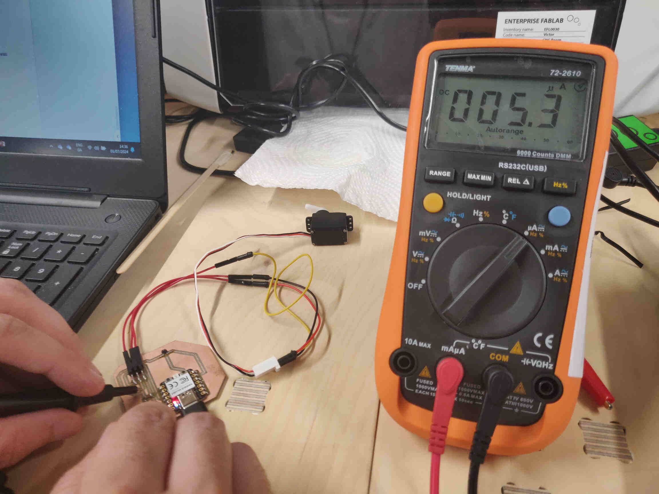
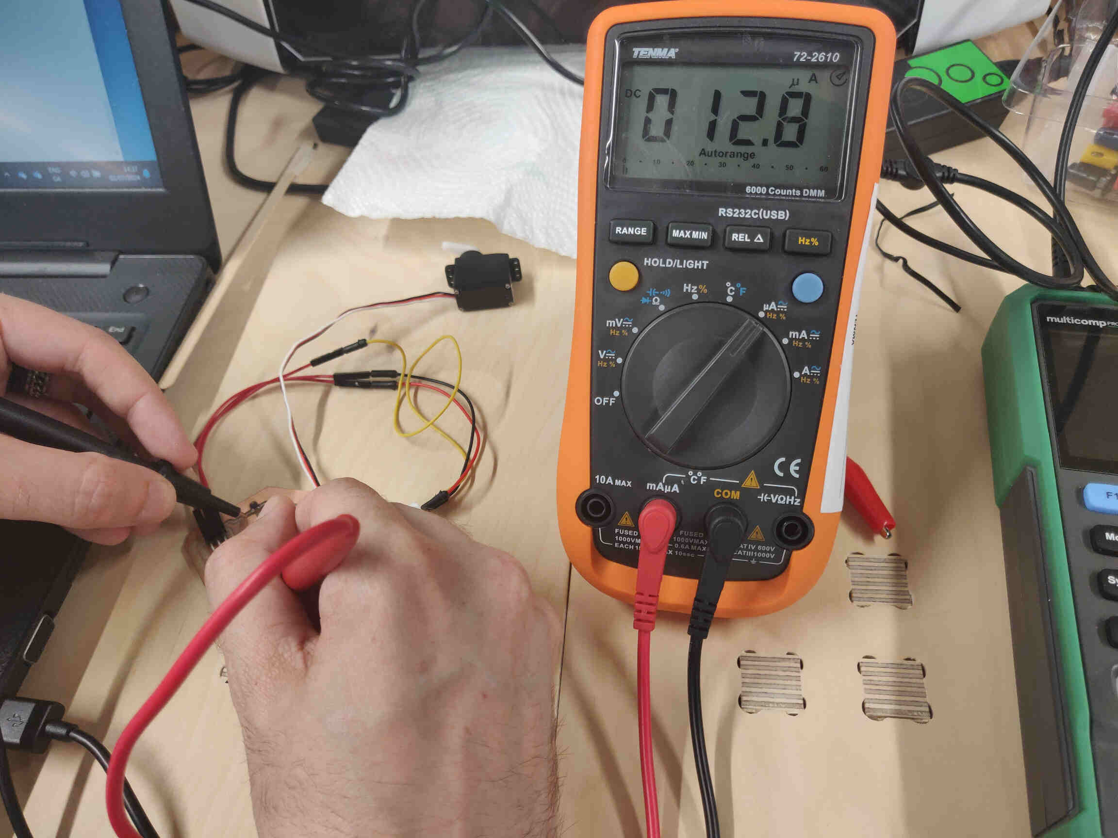
Multimeter: Servo Connection while inactive: 4.6 (V) - 5.6 (A)
Multimeter: Servo Connection while active: 1.8 (V) - 5.7(A)
Multimeter: Hall Effect Connection while inactive: 0.4 (V) - 7.6 (A)
Multimeter: Hall Effect Connection while active: 2.2 (V) - 12.5(A)
*(V) = Voltage
*(A) = Amps
How to Measure Watts with a Multimeter Tenma 72-2610 Multimeter Manual
____________
Individual Assignment:
____________
Wednesday Meeting Reflection
Research into EDA Tools
Design your own microcontroller board - We used electronics, now we need to design it. Check component boards - ribbon cables, IDC connector, Buttons, Slide switch, etc. For microcontrollers it’s all about pins and pinouts.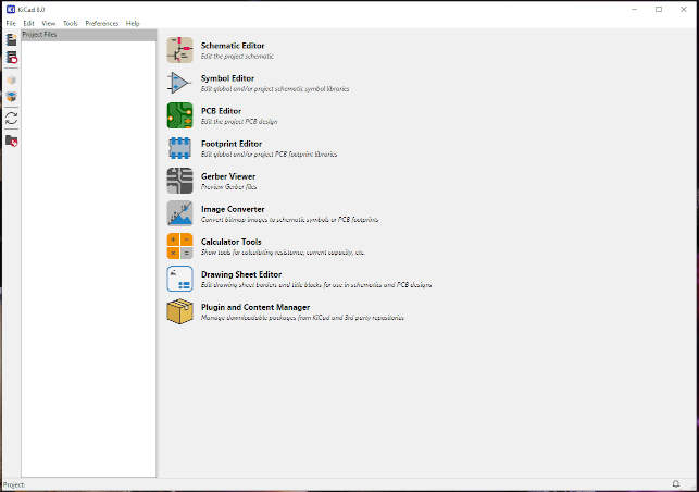

Where should I start? -> ‘Art of Electronics’ - the bible for electronics. Check Tinkercad, KiCad & Virtual Breadboard + Circuit Playground on YouTube. Export your Circuit Designs as an SVG to bring into Modsproject. Schematics and Diagrams. Diagrams are what you download/export and bring into modsproject. Libraries in gitlab - KiCad libraries being the most accurate. SVG-PCB gives examples of the types of PCB designs you may need.

Extra Notes:
Currents (A),Voltage (V)
EDA (Electronic Design Automation)
DRC (Design Rule Check)
Eagle is a powerful EDA tool found in Fusion 360. KiCad is also a powerful EDA Tool.
Simulation - “Digital Simulation isn’t physics, it’s just logic”.


Assignment Progress:
To understand this process of designing electronics, I needed to break down the assignment into all the separate parts and decide which software I would be using to design the concept of my PCB. I would need to pick a software to design the board and circuits such as TinkerCAD, KiCAD or Eagle through Autodesk Fusion 360. After I have all the components lined up and connected, I need to design my board and the layout into something unique and interesting. It doesn’t need to be optimized - in fact, it can be counterintuitive - as long as it works.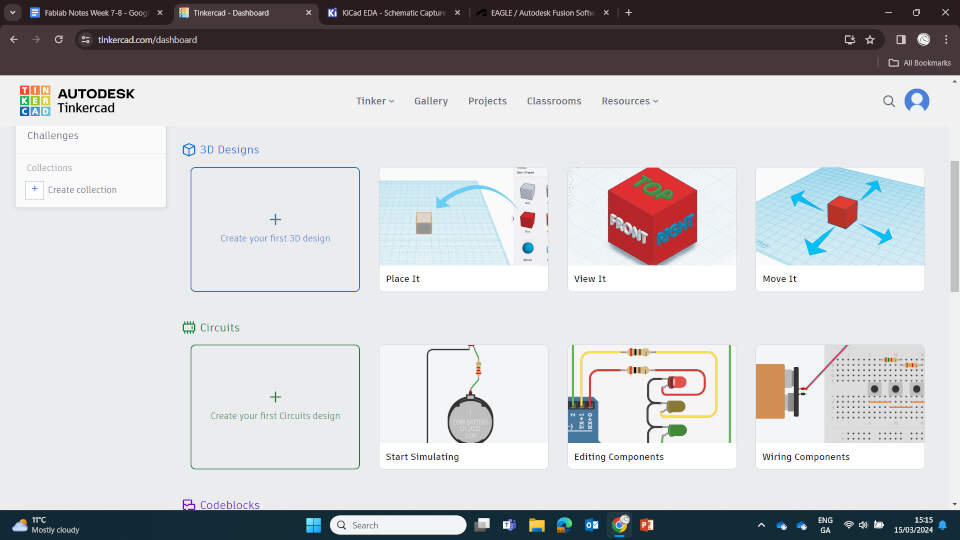
Once the design is done, I would need to download it as an SVG file (a vector file) and bring it into Modsproject.org to setup and begin the milling process onto copper using a Roland DGShape Milling machine. I would also need to create an SVG outline file at the correct measurements to cut out the board. After being milled, I need to assemble all my components and begin the soldering process. After soldering, I will test the traces with a multimeter then connect it to my computer and embed code within Arduino IDE or C+ software. Then if I run a serial communication with another PCB like an Arduino UNO or AtTiny and it works, then that’s the assignment done.
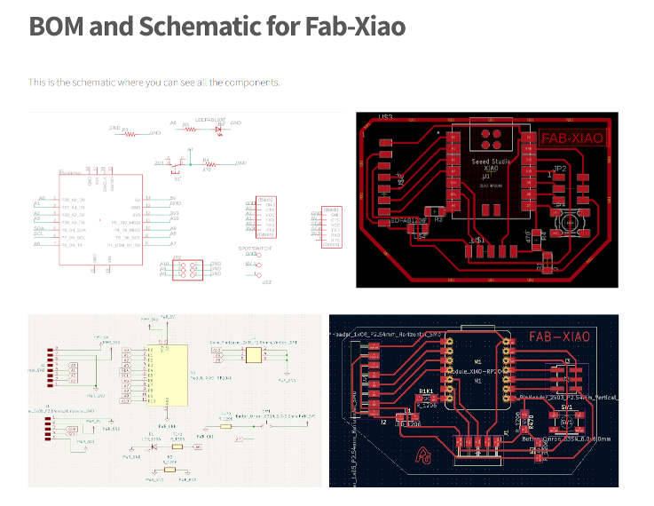
Components Required
Looking back on Week 4 (Electronics Production), if I am to design a PCB with the same functionality of the Quentorres, I will need these types of components: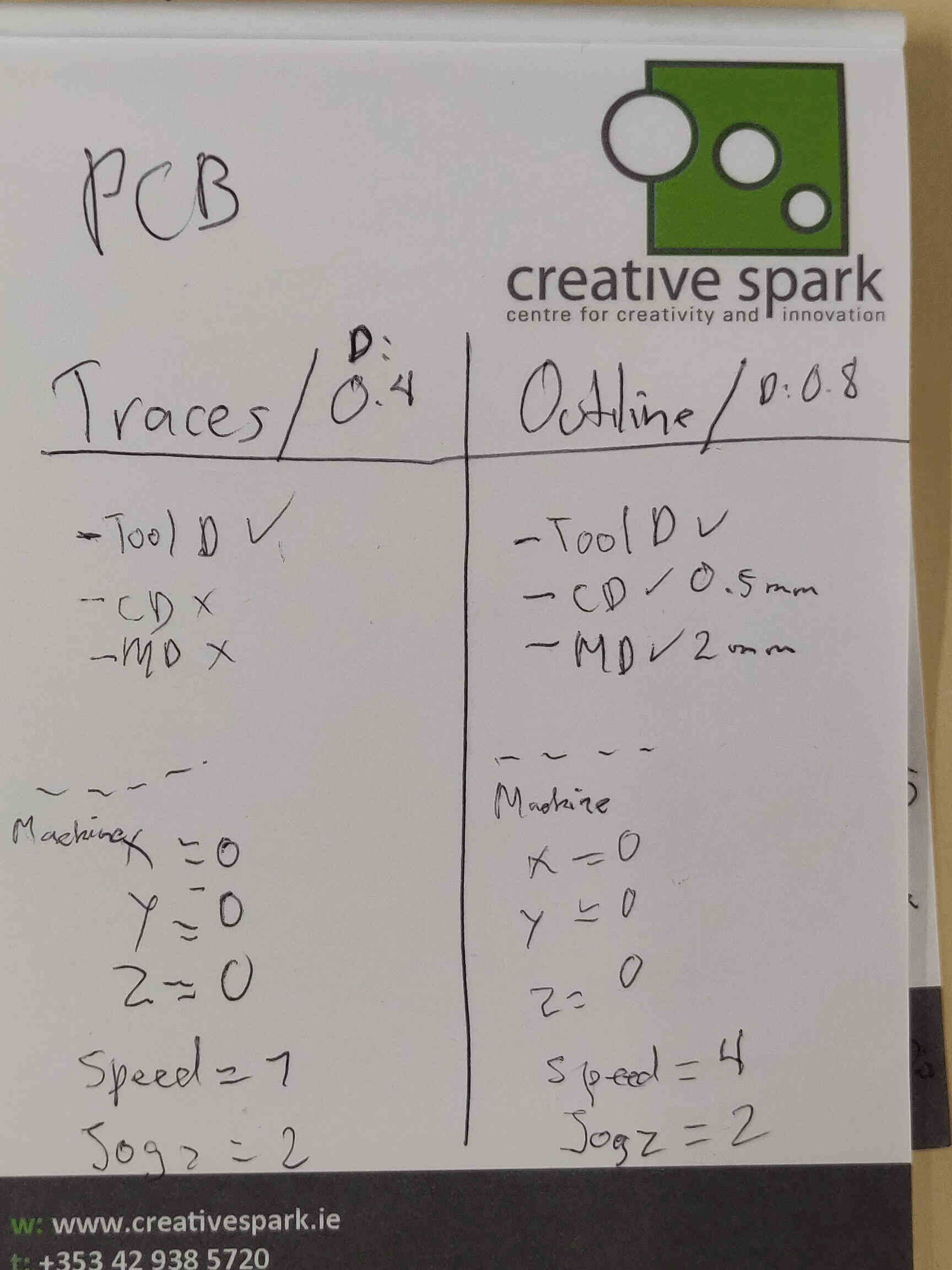
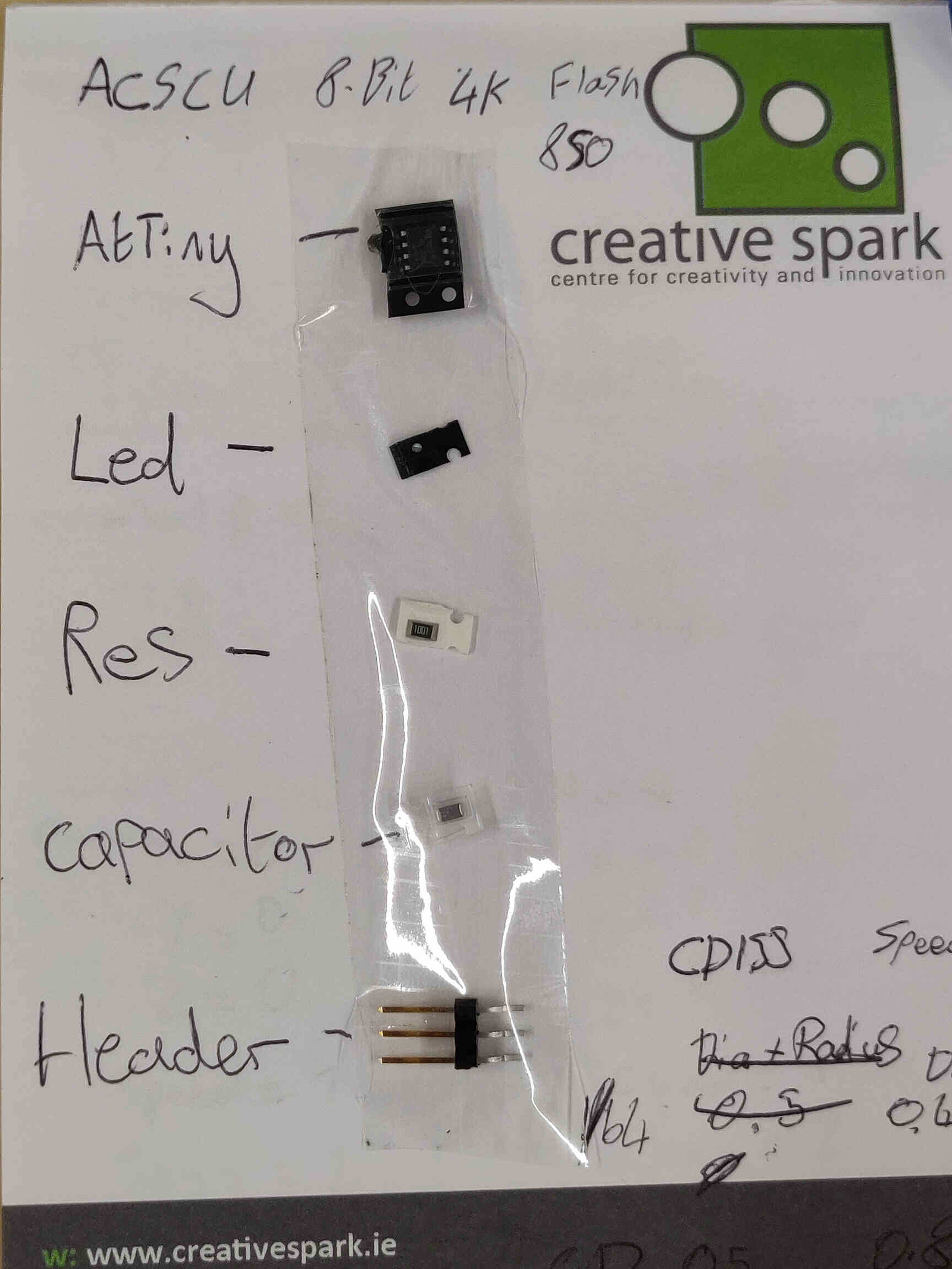
SEEED Studio XIAO RP2040
3x Pin Headers:
CONN HEADER SMD 10POS 1.27mm
CONN HEADER SMD R/A 6POS 2.54mm
CONN HEADER 7POS 0.1 TIN SMD
1x Button:
Tactile Switch SPST-NO Top Actuated Surface Mount
3x LEDs:
LED BLUE CLEAR 1206 SMD (x3)
5x Resistors:
RES 1K OHM 1% 1/4W 1206 (x4)
RES 499 OHM 1% 1/4W 1206
Q. What is an OHM?
Answer: OHM is the unit of electrical resistance in the International System of Units.
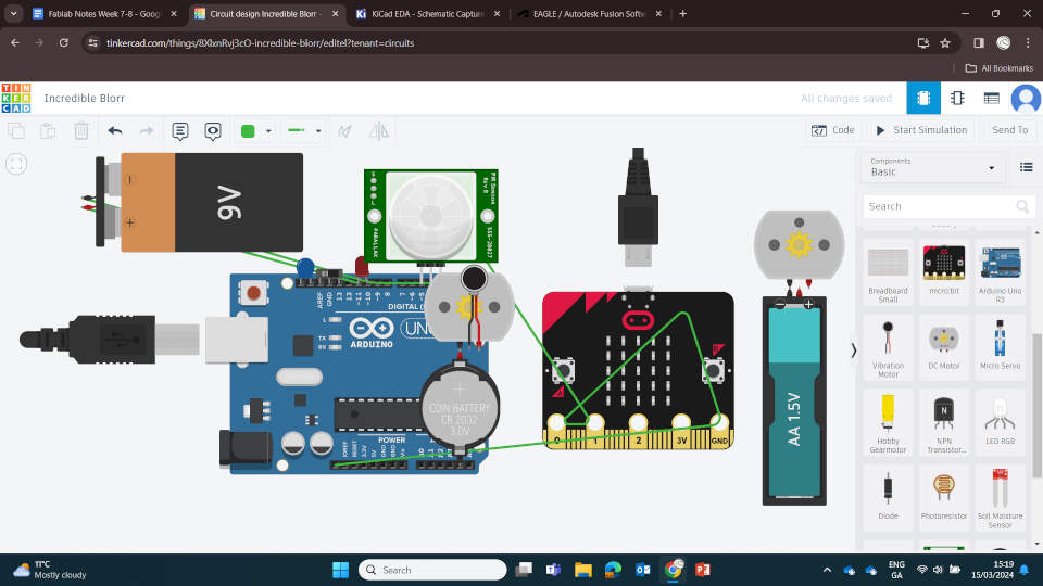
To start off, I played around with TinkerCAD which seems like a fantastic introduction to circuit board design - however it didn’t seem to have the tools I needed to design my own board in the way I’m expected to for this assignment. Either that, or I couldn’t find what I needed.
Moving on to KiCAD, this seemed to be going in the direction I was looking for, showing me a visual representation of what I am making and guides on how to achieve it - even giving me example templates of different types of PCB layouts for different actions or jobs.
You can download KiCAD from HERE.
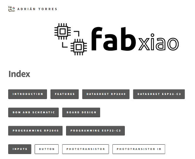
For research into this project, I reviewed the Week 6 Electronics Design Fab Academy websites belonging to Adrain Torres, Ani Liu and Kai Zheng. Adrian’s notes were very detailed and had essentially everything you need - though it was all a bit too technical for my non-electrical savvy brain. This is where Ani’s website came in great use. It was not too descriptive, but straight and to the point, she showed me the whole process laid out in simple steps.
In terms of what unique design to use, I am still unsure. I’d like to use something cool or funny as a background but not sure if I want to delve into meme territory. I really like Ani’s concept of using a vectorised face silhouette as a PCB board and would like to try something along those lines. I had first thought of using a phoenix design as a cybernetic bird might look interesting, but may be too complex or awkward. If I can’t think of a design to use, then I’ll resort to using the Little Buddy logo created during Week 3 as a fall back. Kai’s was very interesting to look at and see his process, however it isn’t a process I intend on using.
This DEMO Featured HERE on this week's Fab Academy assignment page was a great way to show the simplicity of the process without using narration.
First step is to open up KiCAD after it is installed on your computer, and go to File -> New Project, then Save project. Once that’s done, you should now be able to see your new files in KiCAD, a kicad.pcb file and a kicad.sch file. Double click on your ‘kicad.sch’ file to open up the Schematic Editor.
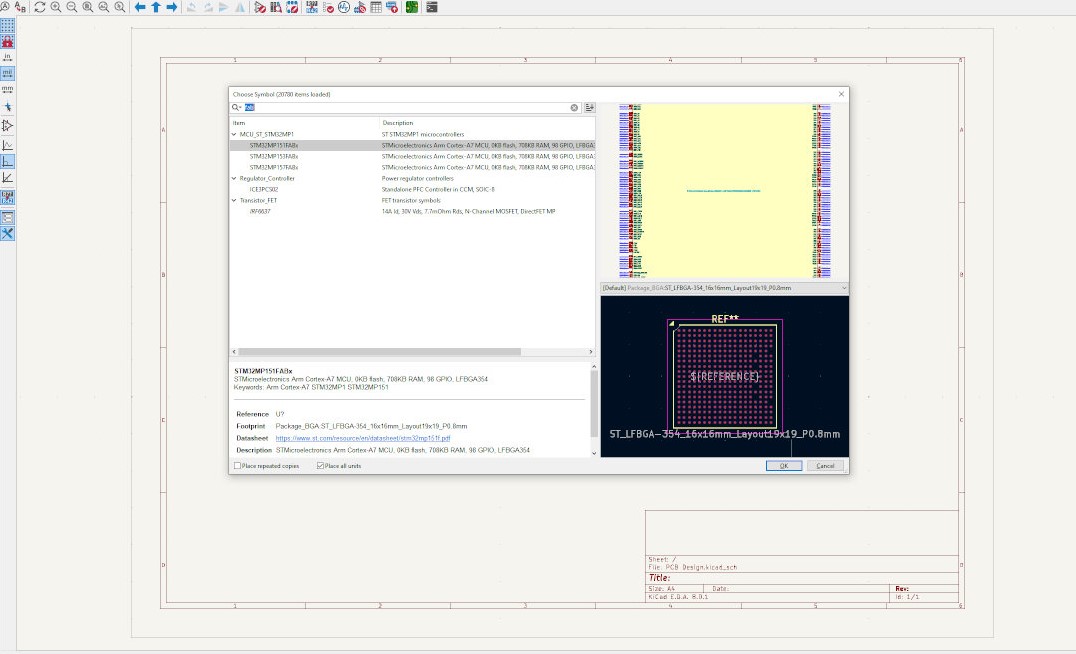
This is the Schematic Editor where we design the schematics for our PCB board. On the right hand side, you can see different types of components set as design tools. To see the names of these tools, hover your mouse over them. Click on the one that’s called ‘Add Symbol (A)’ and then it will start to download the necessary libraries. A menu will pop up - this is your inventory, which is updated with new schematics from other users.
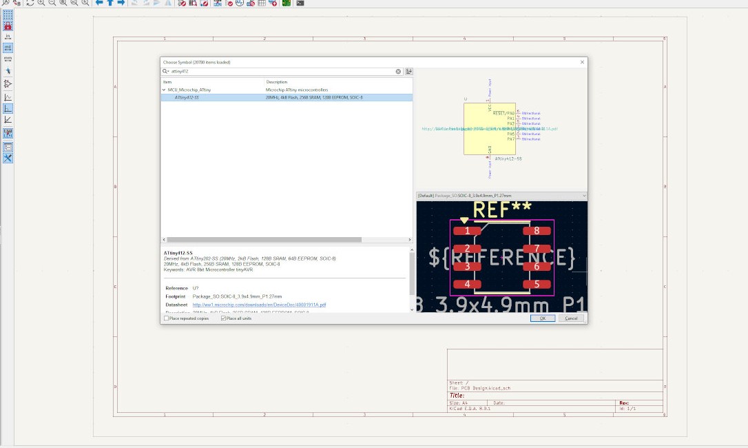
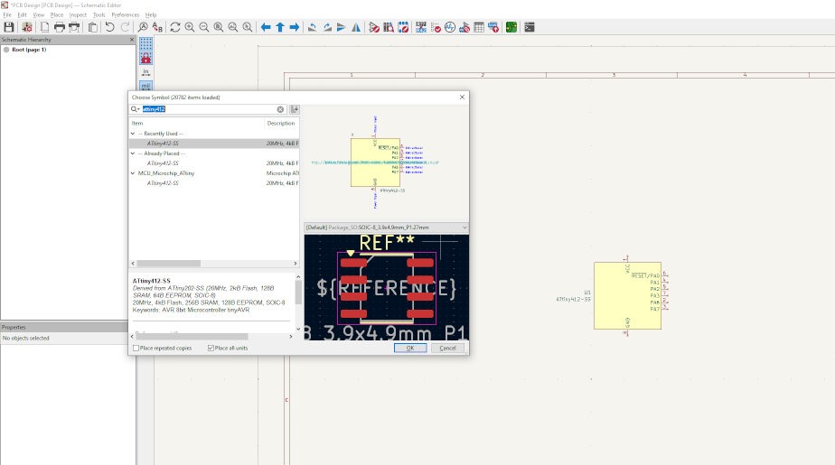
In Adrian’s video he searched ‘fab’ in the Library inventory and got plenty of results for component schematics, however these options did not appear for me when I did the same. He later chose to use the AtTiny schemetics, so I did the same. In your inventory search menu, type ‘attiny412’ and select the one called ‘ATtiny412-SS’. Select OK to add to your schematic board, then drop it somewhere in the middle. NOTE: KiCAD crashed on my first attempt doing this, so you may or may not experience the same.
Next we need to add the POWER and GROUND schematics. To do this, you need the fab library which I don’t have access to yet. To get access follow this link HERE.
This link has the necessary libraries for this project. Download the directory as a zip file and save it. Extract and Rename the folder to ‘fab’ for ease of use.
Now go back to KiCAD and go to Preferences -> Manage Symbol Libraries. Then select the folder near the bottom of the pop-up menu and ‘Add Existing Library’. Then select the file ‘fab.kicad_sym’ found in your new fab folder. Afterwards I went to Tools -> Assign Footprints -> Click Icon above that says ‘Manage footprint libraries’ -> select and add ‘fab.pretty’ folder as footprint library.
NOTE: The gitlab notes say you need to go to Preferences -> ‘Manage Footprint Libraries’ and add ‘fab.pretty’ as footprint library BUT that no longer seems to be an option in KiCAD 8.0 as it’s been moved.
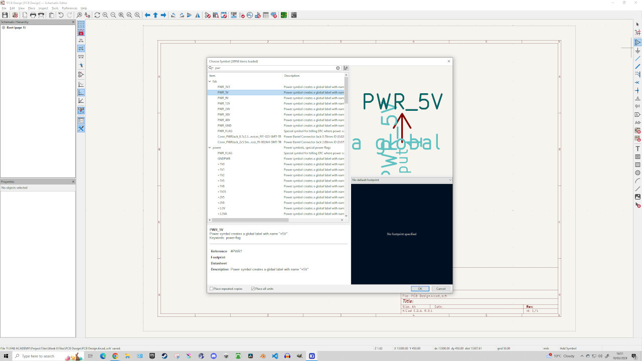
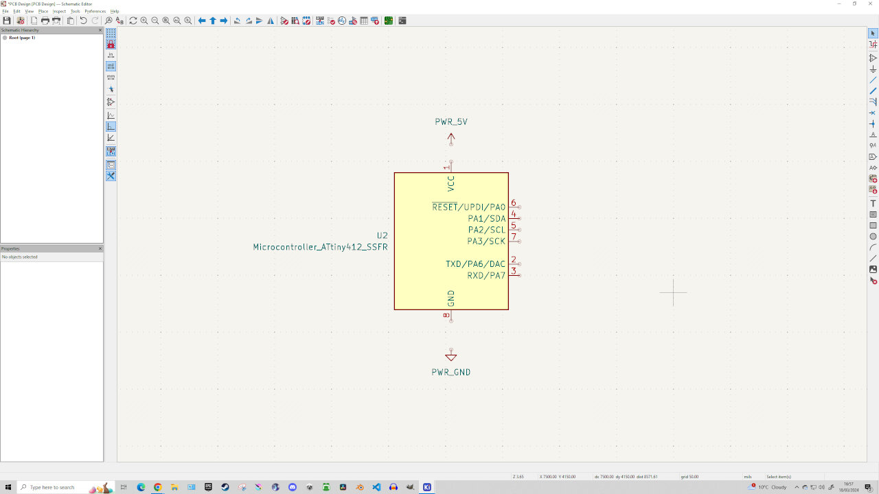
With that done, we now have access to the fab libraries and can now place our POWER component. Simply open up the Library inventory menu (by clicking on the Add Symbol tool) and type in ‘pwr’ and select ‘PWR_5V’ in the fab library. Place it ABOVE your AtTiny schematic and do the same for ‘PWR_GND’ except placing it BELOW the AtTiny. NOTE: Now that we have the fab libraries, it may be worth deleting the original AtTiny we placed and replacing it with the AtTiny412 microcontroller found in the fab libraries.
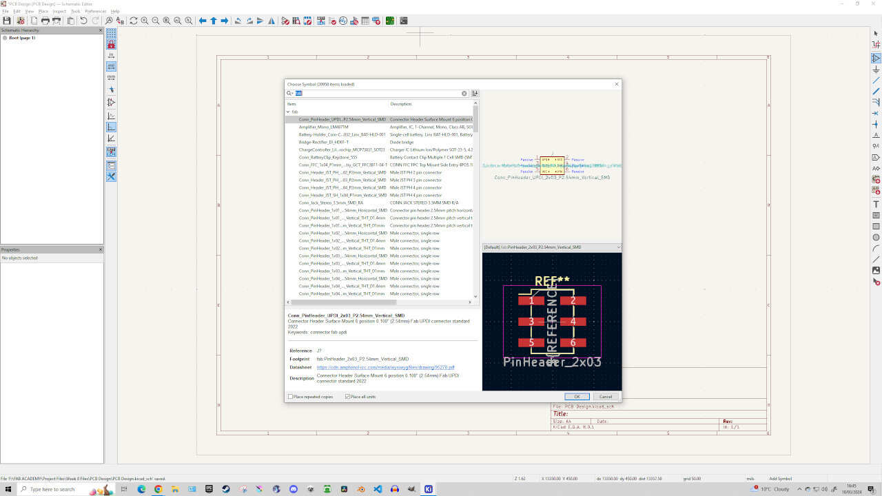
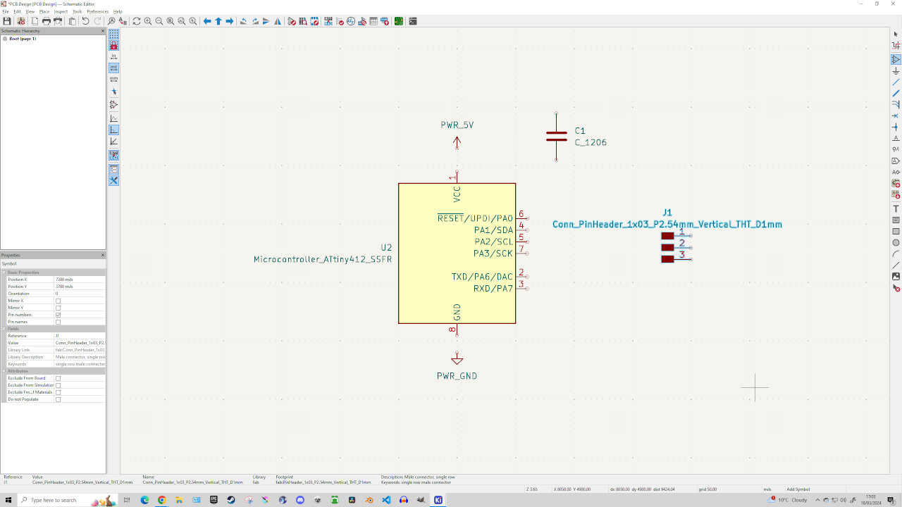
Now we need to add a Capacitor. Under the fab libraries, select ‘C_1206’ and add it to the top-right of your AtTiny board. For the Connector, search in the fab libraries and select the one labelled ‘PinHeader_1x03_P2.54mm_Vertical_THT_D1mm’ and add it to the right of your microcontroller.
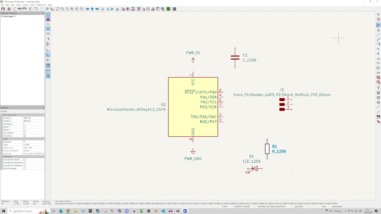
Now we need to add LEDs and a Resistor. First off, under the fab libraries look for the resistor labeled ‘R_1206’ and add it to the bottom right of the microcontroller. LED is labeled ‘LED_1206’, add that one just below your Resistor. With our components placed, we now go through the ‘wiring’ process of connecting them all together.
On the right side of KiCAD select the tool called ‘Add Wire’. This will give you a drawing tool that you can use to connect your components correctly. Simply start drawing the connection at the top of your microcontroller (where it’s labeled ‘VCC’) and connect it to your PWR_5V. Then draw the connection between the GND and PWR_GND.
NOTE: You can create your own path corners by clicking on the workspace while drawing wires.
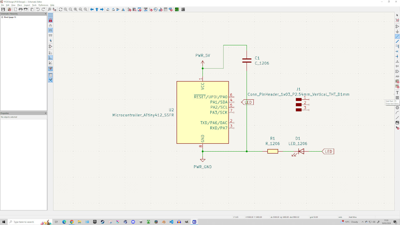
Now draw a wire connecting the PWR_5V to the C_1206 Connector, as well as PWR_GND to the C_1206 Connector. You can click anywhere on the pre-existing wires to create another wired connection. You can select the Resistor and press ‘R’ to rotate it horizontally, making it far easier to create wiring paths and keep your schematics nice and tidy. Now we need to make Labels.
Select the tool called ‘Add Global Labels’, call it ‘LED’ and select OK. Position it next to the microcontroller pin labeled ‘4’. Then copy and paste it (using Ctrl+C and Ctrl+V) and drag the second LED to the right side of your LED component. Try to position your resistor, LED and label in a straight line as seen below, then add wires starting from the PWR_GND to connect all three. In the Resistor properties, you can rename the Values section to ‘1K’.
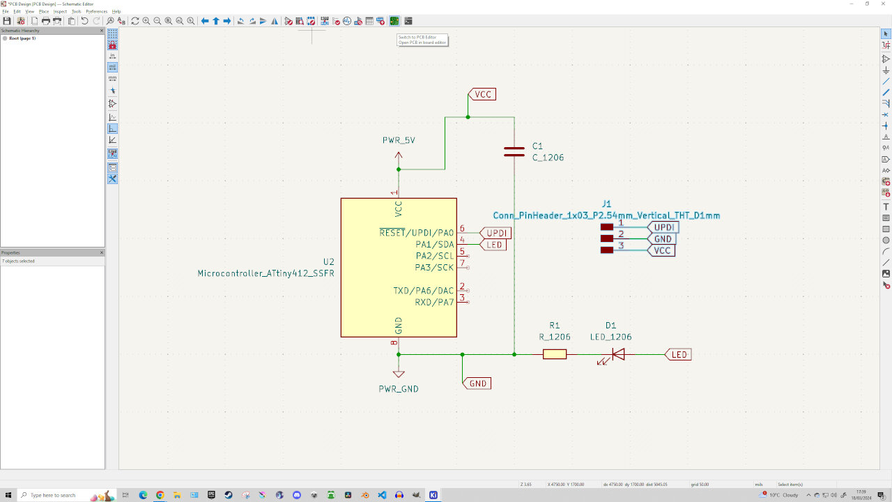
Now we need to add several new labels. Add labels called ‘UPDI’, ‘VCC’ and ‘GND’ and place them to the right of your CONN HEADER (Pin Header) - then make a duplicate of each. It will be difficult to describe where to position all these new labels and components, so try to use the screenshots as examples for positioning. Once positioned, wire them all up as seen in the screenshot and that is essentially your schematic done! Congrats!
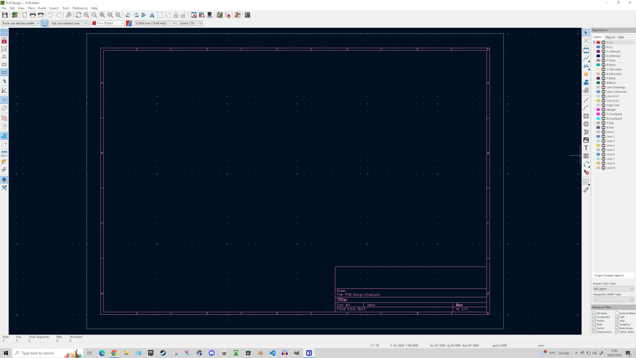
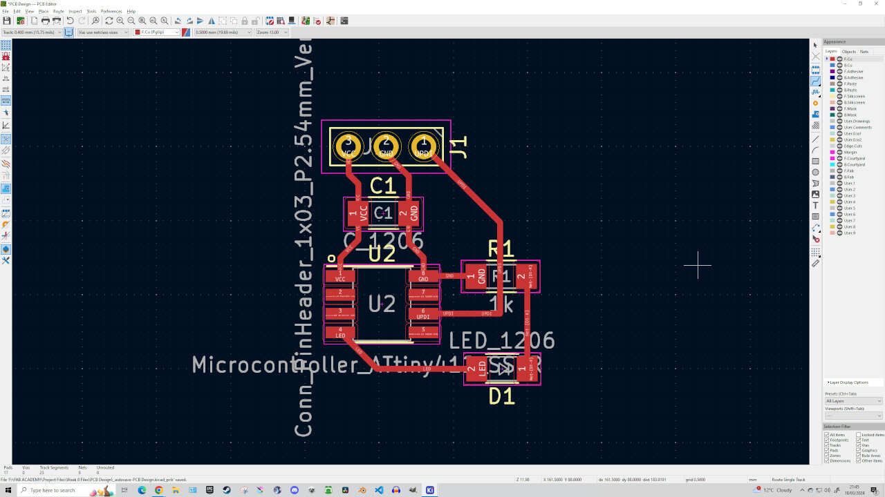
Once you’re ready to move on, click the green icon above your workspace to open the PCB Editor. In the PCB Editor there will be a brown & green icon called ‘Update PCB from Schematic’ - click on this to have your newly made schematic be brought into the PCB Editor. You’ll most likely have to rearrange your board in the PCB Editor as your schematic seems all jumbled up with wires crossed upon updating. Try to follow the positioning through screenshots below. If you think it looks confusing and jumbled - I totally agree.
NOTE: Around this time in Adrian’s tutorial, he ran into trouble as his AtTiny board seemed to be recognized as a Studio Xiao RP2040 board which totally conflicted with his design, so he returned to the schematic editor and replaced his microcontroller with a different AtTiny board. However, when I updated my PCB Editor, there was no issue and it seemed to recognize my board. Because of this, I didn’t feel the need to return to the schematic editor but this may be an issue for some.
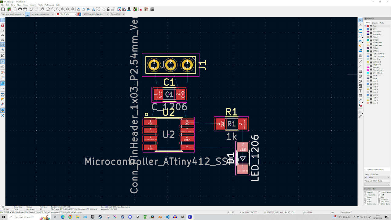
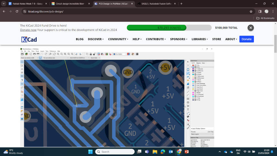
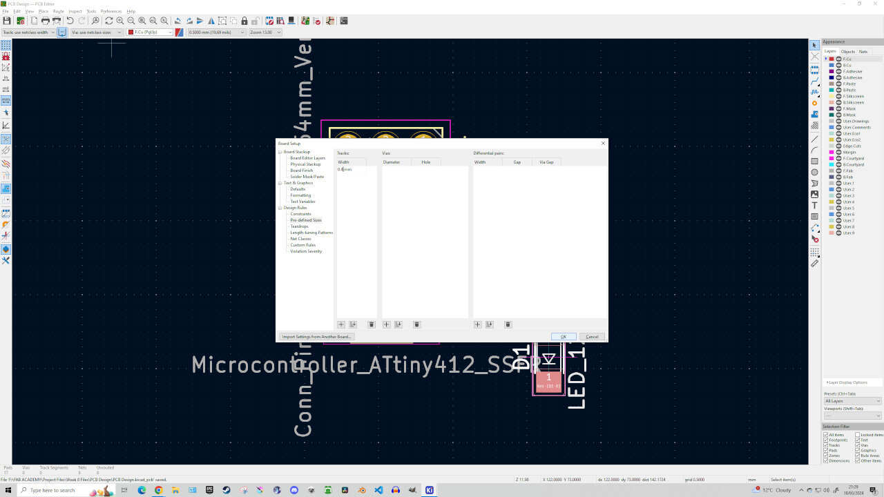
On the top left corner of the workspace, click the drop-down menu that says ‘Track: use netclass width’ then click on ‘Edit: pre-defined Sizes’ to open the Board Setup menu. Hit the ‘+’ button below the Tracks tab, then enter ‘0.4mm’ then hit OK. Now click the drop-down menu that says ‘Track: use netclass width’ then click on ‘0.4mm’. This will increase the width of our tracks. Now press the X key or click the KiCAD tool ‘Route Tracks’ (on the right sidebar) and draw along the thin blue lines along your PCB. Make sure they are not overlapping! However you can pass a trace through a component such as the LED or Resistor, as long as it’s not touching the other paths.
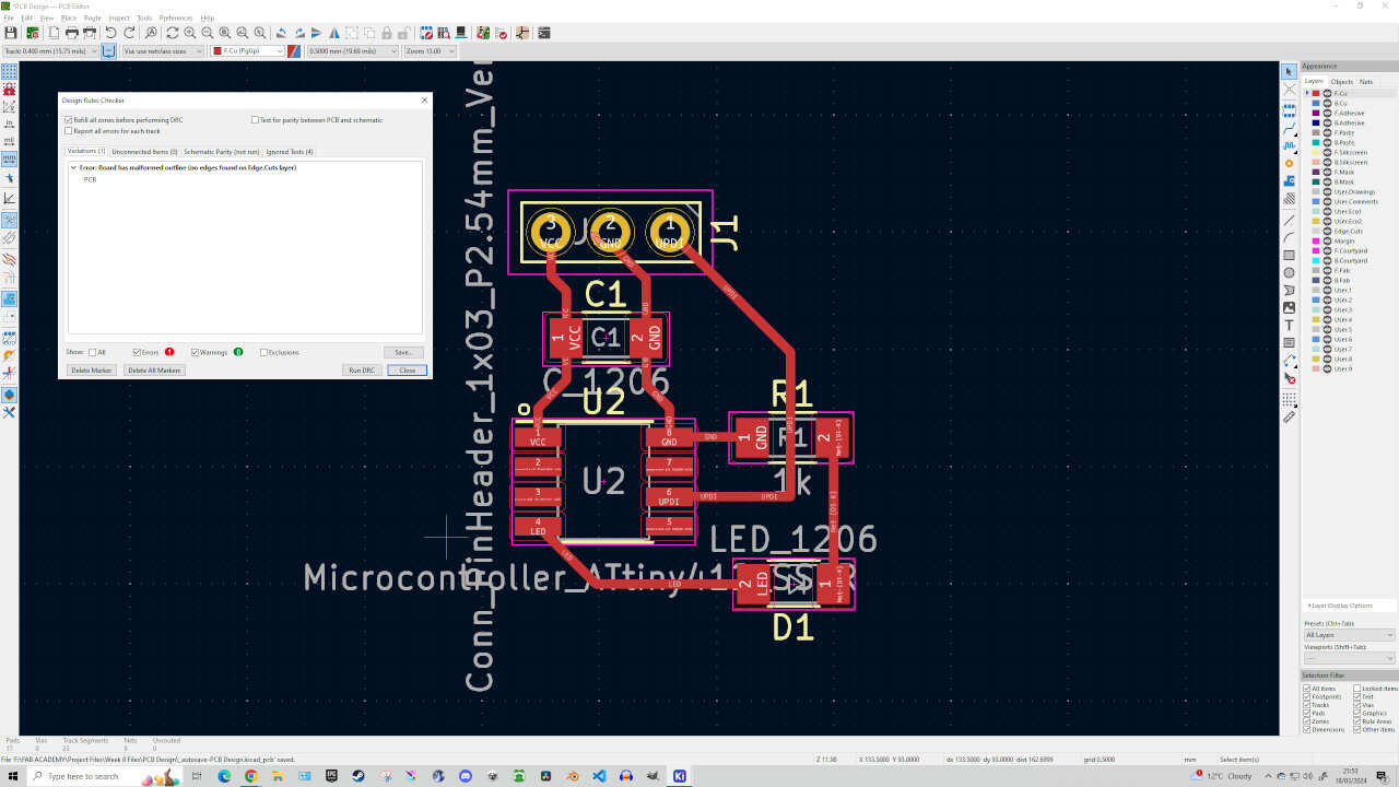
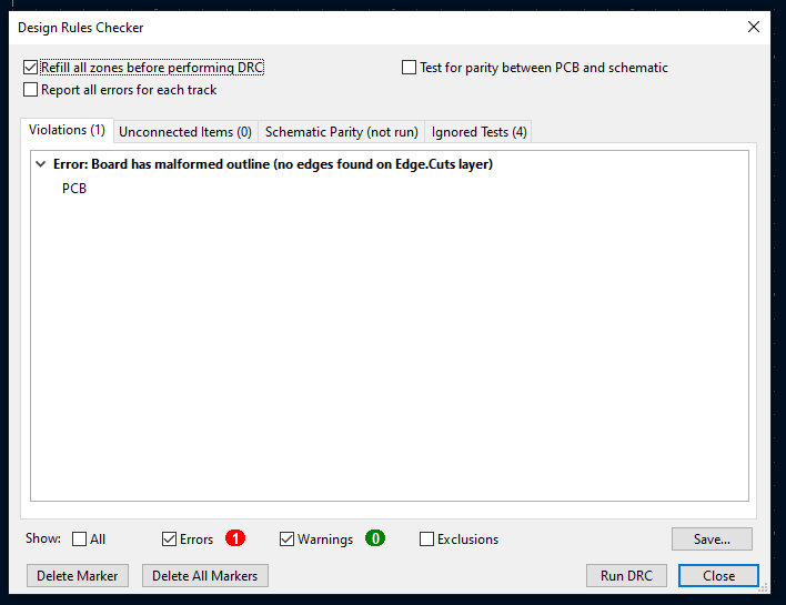
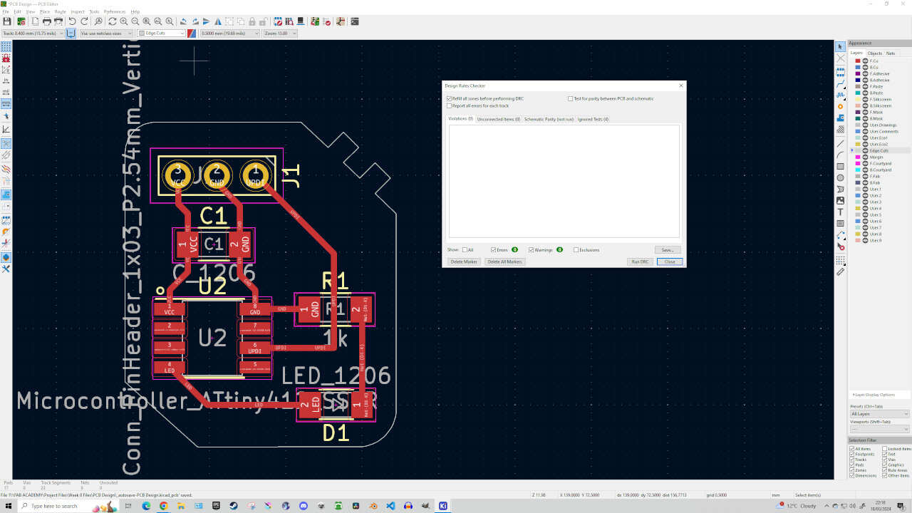
Once you finish making your traces, look at the top of KiCAD and go to ‘Inspect’ -> ‘Design Rules Checker’ -> ‘Run DRC’. This will let you know if you’ve broken any design rules which may lead to an unsuccessful milling. If you run it at this point, you should have 1 error - ‘no edges found on Edge.Cuts layer’. Meaning, it’s now time to cut the other layer of our PCB, allowing the mill to cut the board out.
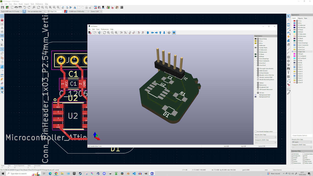
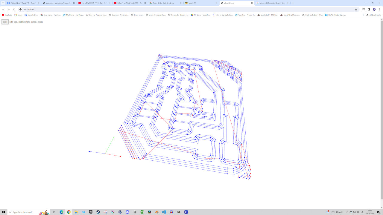
Select the Edge.Cuts layer on the right hand side, then draw the cutout of your board using the Draw Line tool or Draw Arc tool. Once you’ve finished cutting your outline, run the test again. Go to ‘Inspect’ -> ‘Design Rules Checker’ -> ‘Run DRC’. If everything has been cut cleanly then it should come up with no errors. If you go to ‘View’ -> ‘3D Viewer’, you should be able to see a 3D model of what your PCB will look like!
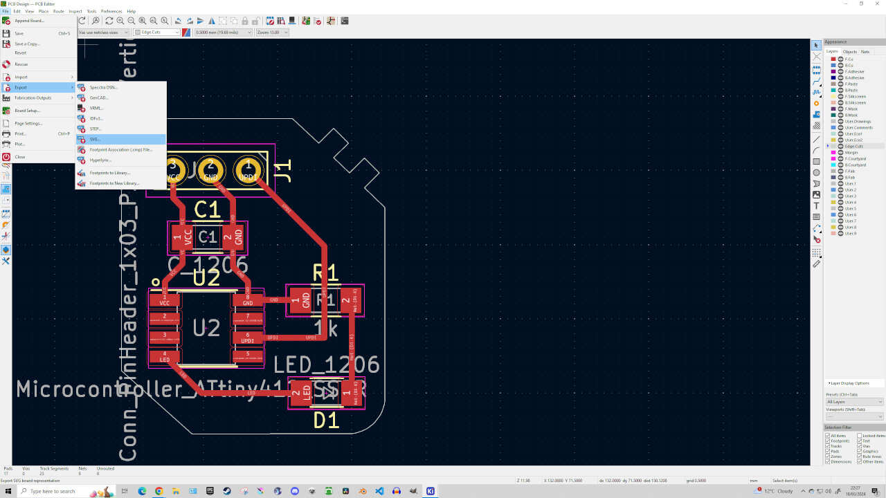
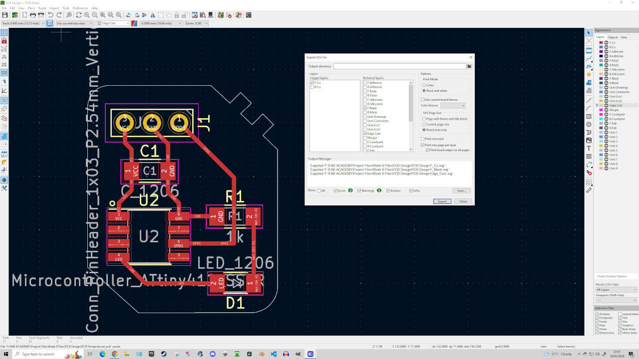
Finally, you are ready to export! In the PCB Editor go to File -> Export -> Export as SVG. In the Copper layer only tick the box that says ‘F.Cu’ and in Technical layers tick the boxes for ‘F.Mask’ and ‘Edge.Cuts’. ALSO make sure you tick ‘Black and White’, ‘Board Area Only’, ‘Print one page per layer’ & ‘Print Board Edges on all pages’, then hit Export.
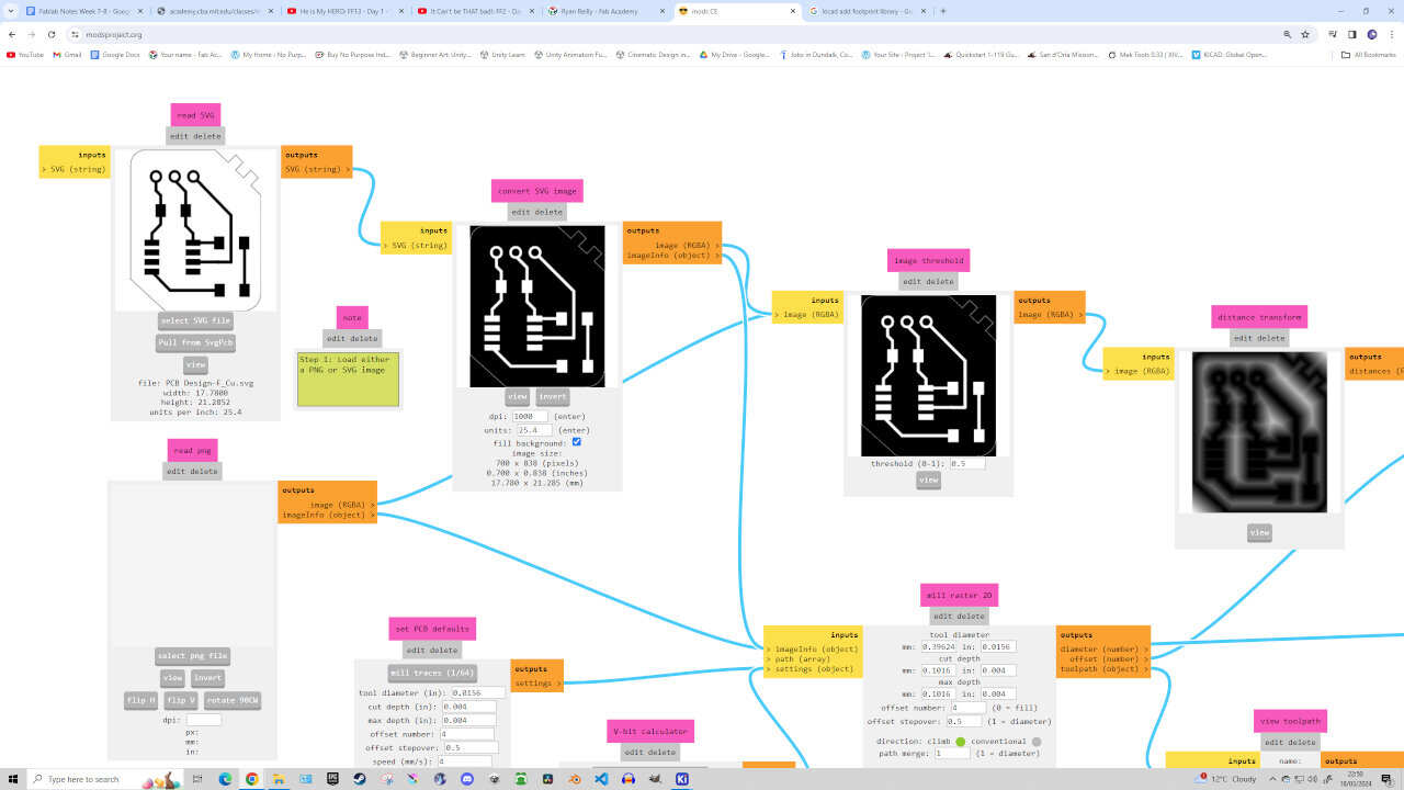
Go to Select SVG file and open your ‘F.Cu’ SVG file. In the second box to the right showing your image, click on ‘Invert’ to swap the blacks and whites. In the ‘Set PCB defaults’ box, click ‘mill traces (1/64)’ if you're using a 1/64 End Mill, then in the ‘mill raster 2D’ box, click ‘Calculate’ to see your toolpath. On the further right you should see two On/Off buttons currently set to ‘Off’. Turn them both on so that you can retrieve the download once hitting ‘Calculate’. NOTE: After selecting my SVG file I noticed the design was too small. This was because it included the size of the component names. To remedy this, go back into PCB Editor and delete the names that are stretching out the image. Re-Export it and try selecting your file in modsproject again.
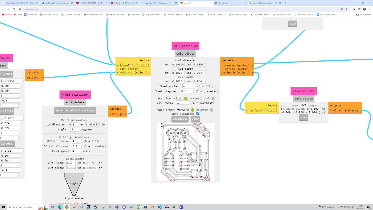
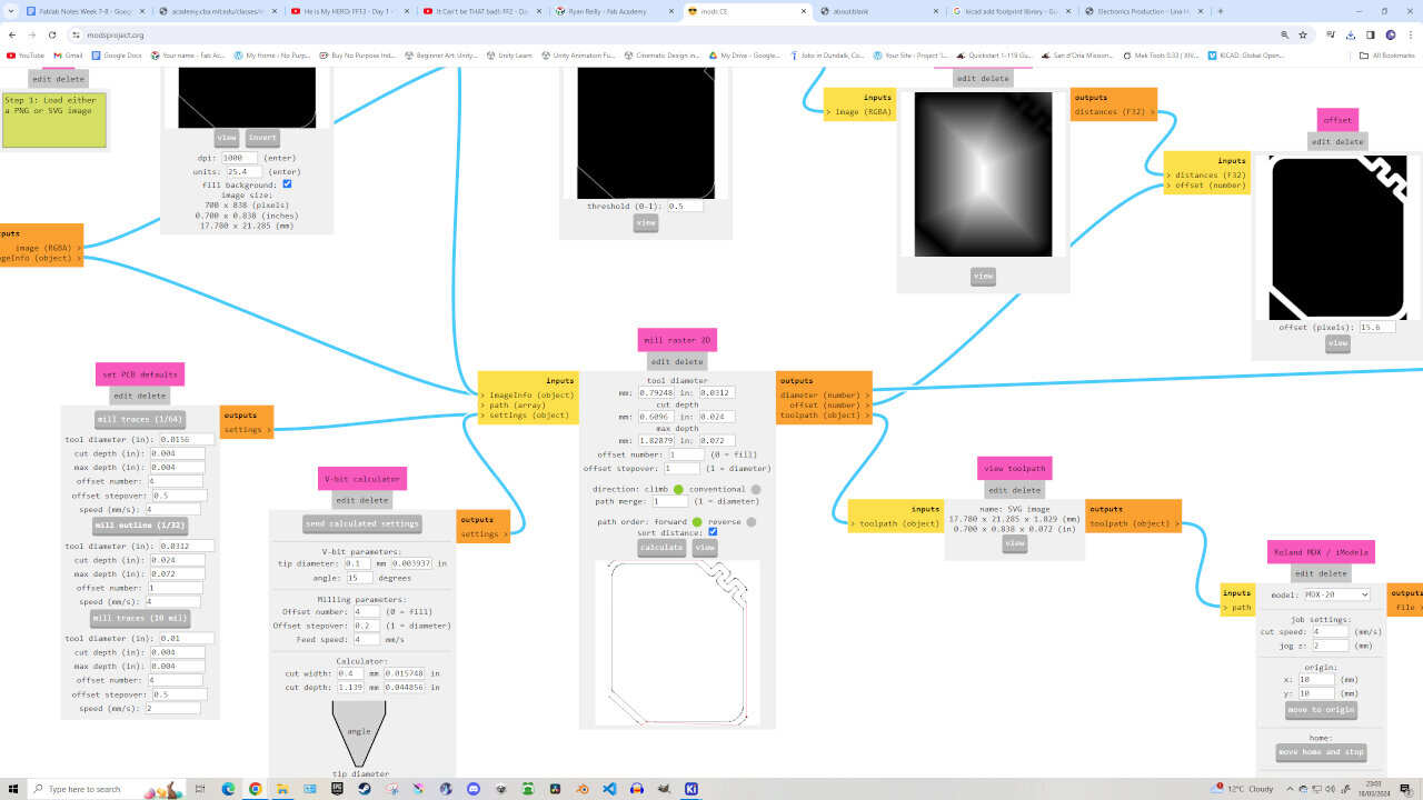
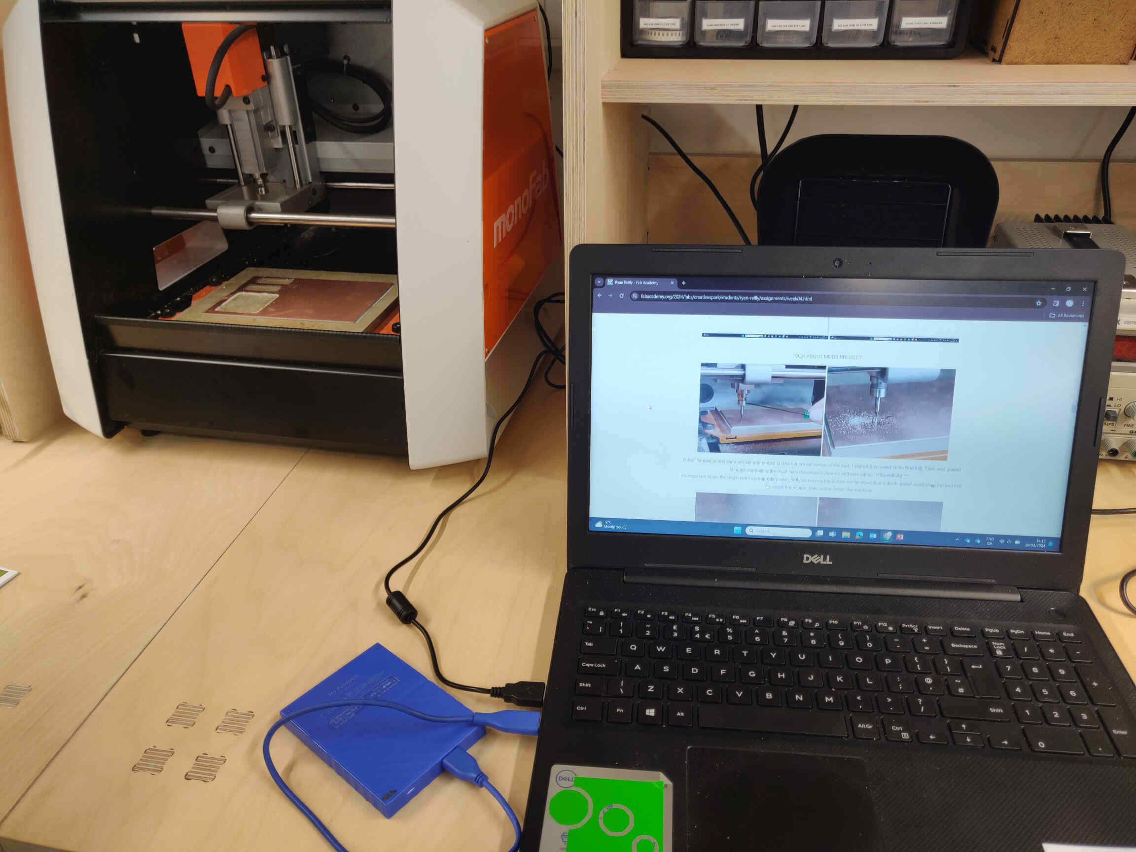
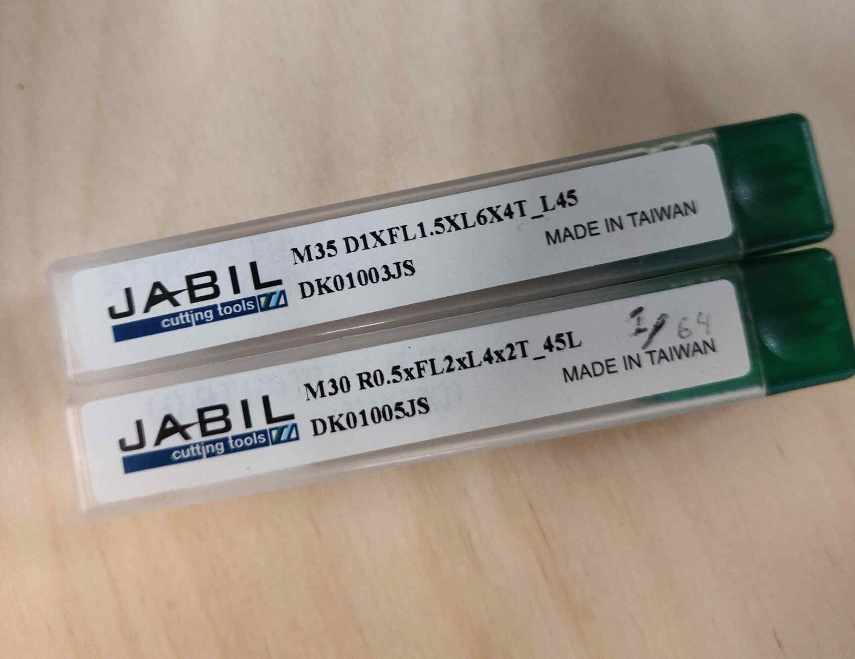
Repeat this process for the ‘Edge.Cuts’ file, except click ‘mill traces (1/32)’ instead of 64 and set up for 1/32 End Mill Outline Cuts. For a more detailed look at the specifics of milling,
go back to my Week 4 Documentation.
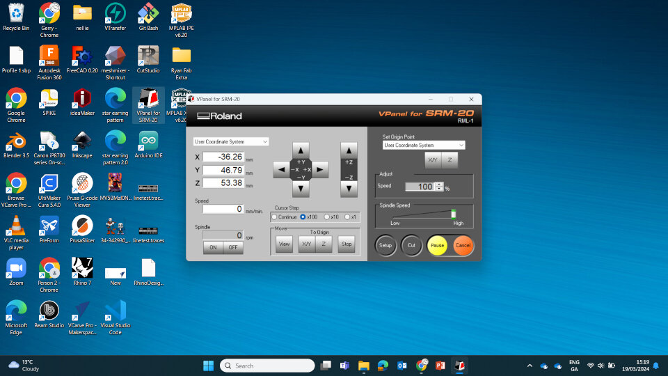
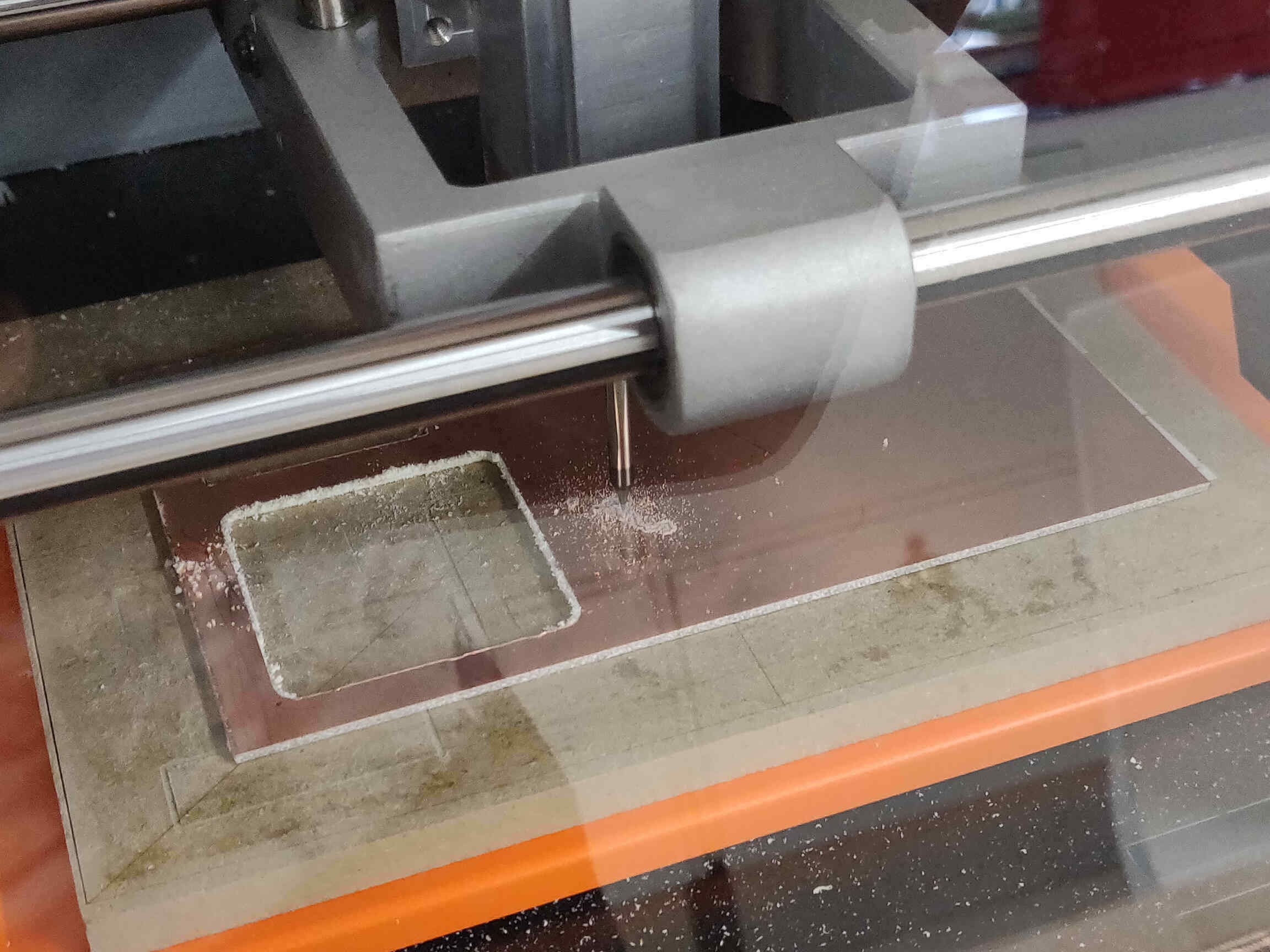
Once the Milling is done using the Roland SRM-20 and VPanel Software, the components are ready to be soldered onto the board, then tested with a Multimeter.
Here are several examples of those PCB's in action after being tested:
Modsproject is a very helpful tool that made the Design->Production process very easy. But it's worth noting that the site is 'finicky' and awkward to navigate. Overall it's well organized but for a new user it can be slightly confusing. Many times the toolpath would be improperly calculated due to wrong numbers, forgetting to invert images, clicking the wrong 'on/off' button, etc.
Milling using VPanel is also very user friendly but went something goes wrong, (such as my previous issues with improperly zeroing the Z-axis), no feedback is given, leaving it up to you to solve what the issue is. I love the milling process and would like to return to it - not to create functional circuit boards, but to use EDA tools and milling to create designs & artwork milled into copper using the PCB aesthetic.
Soldering components also became a favourite process of mine as it can be intense with promising results and a lot of finessing. I hope I get to solder some more stuff in the future - it gives me that primal urge to burn / melt things. :D
Activating PCB's / Burning Bootloaders caused a lot of issues for me and stalled a lot of my assignment this week. Thankfully we were given the go-ahead to use Seeed Studio Xiao RP2040 microcontrollers which come pre-activated. At first I believed the assignment asking us to 'Get your board to communicate with a microcontroller' wasn't very clear. After going across the provided material & descriptions, I wasn't sure 'how' that should communicate, whether it was wirelessly across networks, communicate to inputs/outputs, through the serial monitor, etc. It was only later I realised I was overcomplicating what was being asked - making sure the board you designed & produced was fully functional.
![]()
Answer: OHM is the unit of electrical resistance in the International System of Units.
To start off, I played around with TinkerCAD which seems like a fantastic introduction to circuit board design - however it didn’t seem to have the tools I needed to design my own board in the way I’m expected to for this assignment. Either that, or I couldn’t find what I needed.
Moving on to KiCAD, this seemed to be going in the direction I was looking for, showing me a visual representation of what I am making and guides on how to achieve it - even giving me example templates of different types of PCB layouts for different actions or jobs.
You can download KiCAD from HERE.
For research into this project, I reviewed the Week 6 Electronics Design Fab Academy websites belonging to Adrain Torres, Ani Liu and Kai Zheng. Adrian’s notes were very detailed and had essentially everything you need - though it was all a bit too technical for my non-electrical savvy brain. This is where Ani’s website came in great use. It was not too descriptive, but straight and to the point, she showed me the whole process laid out in simple steps.
In terms of what unique design to use, I am still unsure. I’d like to use something cool or funny as a background but not sure if I want to delve into meme territory. I really like Ani’s concept of using a vectorised face silhouette as a PCB board and would like to try something along those lines. I had first thought of using a phoenix design as a cybernetic bird might look interesting, but may be too complex or awkward. If I can’t think of a design to use, then I’ll resort to using the Little Buddy logo created during Week 3 as a fall back. Kai’s was very interesting to look at and see his process, however it isn’t a process I intend on using.
PCB Design Process
When creating my own PCB design on KiCAD, I followed Adrian Torres’s guide for using KiCAD to create a PCB design, which can be seen HERE.This DEMO Featured HERE on this week's Fab Academy assignment page was a great way to show the simplicity of the process without using narration.
First step is to open up KiCAD after it is installed on your computer, and go to File -> New Project, then Save project. Once that’s done, you should now be able to see your new files in KiCAD, a kicad.pcb file and a kicad.sch file. Double click on your ‘kicad.sch’ file to open up the Schematic Editor.
This is the Schematic Editor where we design the schematics for our PCB board. On the right hand side, you can see different types of components set as design tools. To see the names of these tools, hover your mouse over them. Click on the one that’s called ‘Add Symbol (A)’ and then it will start to download the necessary libraries. A menu will pop up - this is your inventory, which is updated with new schematics from other users.
In Adrian’s video he searched ‘fab’ in the Library inventory and got plenty of results for component schematics, however these options did not appear for me when I did the same. He later chose to use the AtTiny schemetics, so I did the same. In your inventory search menu, type ‘attiny412’ and select the one called ‘ATtiny412-SS’. Select OK to add to your schematic board, then drop it somewhere in the middle. NOTE: KiCAD crashed on my first attempt doing this, so you may or may not experience the same.
Next we need to add the POWER and GROUND schematics. To do this, you need the fab library which I don’t have access to yet. To get access follow this link HERE.
This link has the necessary libraries for this project. Download the directory as a zip file and save it. Extract and Rename the folder to ‘fab’ for ease of use.
Now go back to KiCAD and go to Preferences -> Manage Symbol Libraries. Then select the folder near the bottom of the pop-up menu and ‘Add Existing Library’. Then select the file ‘fab.kicad_sym’ found in your new fab folder. Afterwards I went to Tools -> Assign Footprints -> Click Icon above that says ‘Manage footprint libraries’ -> select and add ‘fab.pretty’ folder as footprint library.
NOTE: The gitlab notes say you need to go to Preferences -> ‘Manage Footprint Libraries’ and add ‘fab.pretty’ as footprint library BUT that no longer seems to be an option in KiCAD 8.0 as it’s been moved.
With that done, we now have access to the fab libraries and can now place our POWER component. Simply open up the Library inventory menu (by clicking on the Add Symbol tool) and type in ‘pwr’ and select ‘PWR_5V’ in the fab library. Place it ABOVE your AtTiny schematic and do the same for ‘PWR_GND’ except placing it BELOW the AtTiny. NOTE: Now that we have the fab libraries, it may be worth deleting the original AtTiny we placed and replacing it with the AtTiny412 microcontroller found in the fab libraries.
Now we need to add a Capacitor. Under the fab libraries, select ‘C_1206’ and add it to the top-right of your AtTiny board. For the Connector, search in the fab libraries and select the one labelled ‘PinHeader_1x03_P2.54mm_Vertical_THT_D1mm’ and add it to the right of your microcontroller.
Now we need to add LEDs and a Resistor. First off, under the fab libraries look for the resistor labeled ‘R_1206’ and add it to the bottom right of the microcontroller. LED is labeled ‘LED_1206’, add that one just below your Resistor. With our components placed, we now go through the ‘wiring’ process of connecting them all together.
On the right side of KiCAD select the tool called ‘Add Wire’. This will give you a drawing tool that you can use to connect your components correctly. Simply start drawing the connection at the top of your microcontroller (where it’s labeled ‘VCC’) and connect it to your PWR_5V. Then draw the connection between the GND and PWR_GND.
NOTE: You can create your own path corners by clicking on the workspace while drawing wires.
Now draw a wire connecting the PWR_5V to the C_1206 Connector, as well as PWR_GND to the C_1206 Connector. You can click anywhere on the pre-existing wires to create another wired connection. You can select the Resistor and press ‘R’ to rotate it horizontally, making it far easier to create wiring paths and keep your schematics nice and tidy. Now we need to make Labels.
Select the tool called ‘Add Global Labels’, call it ‘LED’ and select OK. Position it next to the microcontroller pin labeled ‘4’. Then copy and paste it (using Ctrl+C and Ctrl+V) and drag the second LED to the right side of your LED component. Try to position your resistor, LED and label in a straight line as seen below, then add wires starting from the PWR_GND to connect all three. In the Resistor properties, you can rename the Values section to ‘1K’.
Now we need to add several new labels. Add labels called ‘UPDI’, ‘VCC’ and ‘GND’ and place them to the right of your CONN HEADER (Pin Header) - then make a duplicate of each. It will be difficult to describe where to position all these new labels and components, so try to use the screenshots as examples for positioning. Once positioned, wire them all up as seen in the screenshot and that is essentially your schematic done! Congrats!
Once you’re ready to move on, click the green icon above your workspace to open the PCB Editor. In the PCB Editor there will be a brown & green icon called ‘Update PCB from Schematic’ - click on this to have your newly made schematic be brought into the PCB Editor. You’ll most likely have to rearrange your board in the PCB Editor as your schematic seems all jumbled up with wires crossed upon updating. Try to follow the positioning through screenshots below. If you think it looks confusing and jumbled - I totally agree.
NOTE: Around this time in Adrian’s tutorial, he ran into trouble as his AtTiny board seemed to be recognized as a Studio Xiao RP2040 board which totally conflicted with his design, so he returned to the schematic editor and replaced his microcontroller with a different AtTiny board. However, when I updated my PCB Editor, there was no issue and it seemed to recognize my board. Because of this, I didn’t feel the need to return to the schematic editor but this may be an issue for some.
On the top left corner of the workspace, click the drop-down menu that says ‘Track: use netclass width’ then click on ‘Edit: pre-defined Sizes’ to open the Board Setup menu. Hit the ‘+’ button below the Tracks tab, then enter ‘0.4mm’ then hit OK. Now click the drop-down menu that says ‘Track: use netclass width’ then click on ‘0.4mm’. This will increase the width of our tracks. Now press the X key or click the KiCAD tool ‘Route Tracks’ (on the right sidebar) and draw along the thin blue lines along your PCB. Make sure they are not overlapping! However you can pass a trace through a component such as the LED or Resistor, as long as it’s not touching the other paths.
Once you finish making your traces, look at the top of KiCAD and go to ‘Inspect’ -> ‘Design Rules Checker’ -> ‘Run DRC’. This will let you know if you’ve broken any design rules which may lead to an unsuccessful milling. If you run it at this point, you should have 1 error - ‘no edges found on Edge.Cuts layer’. Meaning, it’s now time to cut the other layer of our PCB, allowing the mill to cut the board out.
Select the Edge.Cuts layer on the right hand side, then draw the cutout of your board using the Draw Line tool or Draw Arc tool. Once you’ve finished cutting your outline, run the test again. Go to ‘Inspect’ -> ‘Design Rules Checker’ -> ‘Run DRC’. If everything has been cut cleanly then it should come up with no errors. If you go to ‘View’ -> ‘3D Viewer’, you should be able to see a 3D model of what your PCB will look like!
Finally, you are ready to export! In the PCB Editor go to File -> Export -> Export as SVG. In the Copper layer only tick the box that says ‘F.Cu’ and in Technical layers tick the boxes for ‘F.Mask’ and ‘Edge.Cuts’. ALSO make sure you tick ‘Black and White’, ‘Board Area Only’, ‘Print one page per layer’ & ‘Print Board Edges on all pages’, then hit Export.
Modsproject.org
Now we go to modsproject.org to get our files ready for milling. Right click anywhere on modsproject site and click on ‘Program’ -> ‘Open Programs’ -> then under ‘MDX mill’ click ‘PCB’ and this will open the setup we require.
Go to Select SVG file and open your ‘F.Cu’ SVG file. In the second box to the right showing your image, click on ‘Invert’ to swap the blacks and whites. In the ‘Set PCB defaults’ box, click ‘mill traces (1/64)’ if you're using a 1/64 End Mill, then in the ‘mill raster 2D’ box, click ‘Calculate’ to see your toolpath. On the further right you should see two On/Off buttons currently set to ‘Off’. Turn them both on so that you can retrieve the download once hitting ‘Calculate’. NOTE: After selecting my SVG file I noticed the design was too small. This was because it included the size of the component names. To remedy this, go back into PCB Editor and delete the names that are stretching out the image. Re-Export it and try selecting your file in modsproject again.
Repeat this process for the ‘Edge.Cuts’ file, except click ‘mill traces (1/32)’ instead of 64 and set up for 1/32 End Mill Outline Cuts. For a more detailed look at the specifics of milling,
go back to my Week 4 Documentation.
Once the Milling is done using the Roland SRM-20 and VPanel Software, the components are ready to be soldered onto the board, then tested with a Multimeter.
Revenge of the Mill...
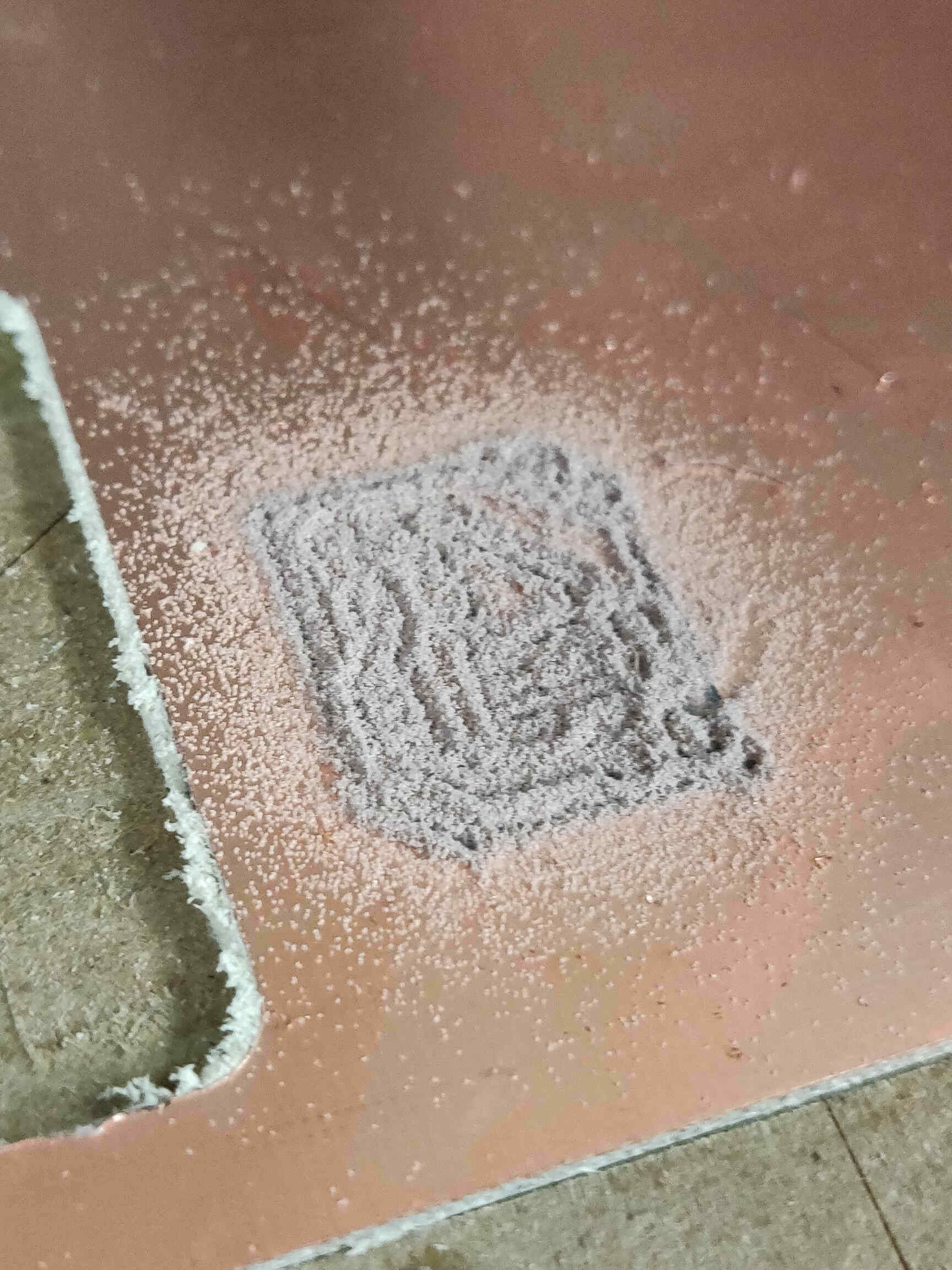
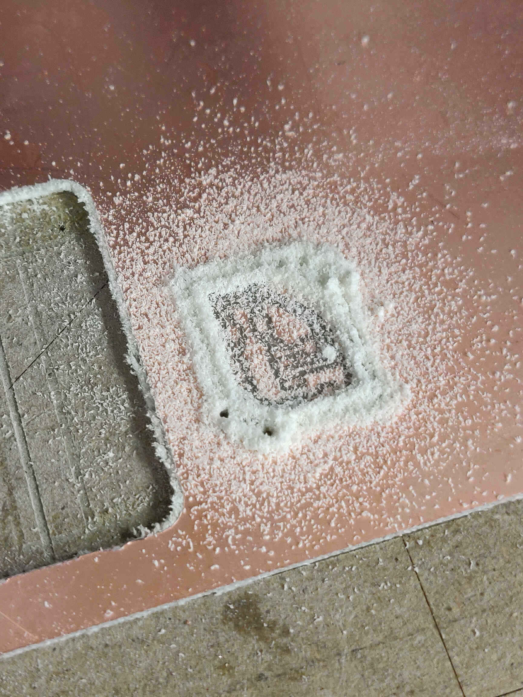
I had a Milling Issue that caused me to be late for my assignment completion. We did eventaully solve it - it was a Zeroing Z-Axis issue. I needed to set the 'home point' for the Z - axis higher (by about -4.50mm) to give the machine more breathing room.
Assignment Update - Attiny to Seeed Studio Xiao
After having a ton of trouble Burning the bootloader with the Attiny, I asked my Fab Academy instructors and co-ordinators for help. Their response was that I’m free to build a board with the Seeed Studio Xiao RP2040 as it comes out of the box pre-bootloaded. So I did the remainder of the assignment with another Quentorres board.____________
Finishing the Assignment
Later on I would produce several of my own PCBs with Seeed Studio Xiao MicroControllers (RP2040 / ESP32-C3) and fuctionality that included Hall Effect Sensors, Servo Motor control, VL53L1X Time of Flight sensing, Wireless communication, etc. These boards were designing using KiCAD, Converted into G-Code with modsproject.org, Milled with the Roland SRM-20 and embedded with code through Arduino IDE and Processing.Here are several examples of those PCB's in action after being tested:
VIDEO SECTION
Functioning Servo Motor
Functioning Hall Effect Sensor
Functioning PushButton/LED ESP32-C3 board
VL53L1X Time of Flight w/ Quentorres RP2040
Processing Data Read from RP2040 controlled Servo
References:
Adrian Torres | Ani Liu | Kai Zhang
Functioning Hall Effect Sensor
Functioning PushButton/LED ESP32-C3 board
VL53L1X Time of Flight w/ Quentorres RP2040
Processing Data Read from RP2040 controlled Servo
____________
References:
Adrian Torres | Ani Liu | Kai Zhang
____________
Conclusion / Reflection
Week 8 was my introduction to EDA tools and making Circuit Board designs entirely from scratch. For this I toyed around with Eagle & TinkerCad but landed on KiCAD as it's UX Design was easy to understand, was user-friendly and there were plenty of guides available. The tutorial to KiCAD that Adrain made during Global Open Time was very helpful. I had no issues when making the PCB through EDA Tools - though the traces were designed to be 0.4mm thick but that resulted in traces being very thin (still functional - just concerning). So I wasn't sure how big I could make the traces before it started to affect the other paths.Modsproject is a very helpful tool that made the Design->Production process very easy. But it's worth noting that the site is 'finicky' and awkward to navigate. Overall it's well organized but for a new user it can be slightly confusing. Many times the toolpath would be improperly calculated due to wrong numbers, forgetting to invert images, clicking the wrong 'on/off' button, etc.
Milling using VPanel is also very user friendly but went something goes wrong, (such as my previous issues with improperly zeroing the Z-axis), no feedback is given, leaving it up to you to solve what the issue is. I love the milling process and would like to return to it - not to create functional circuit boards, but to use EDA tools and milling to create designs & artwork milled into copper using the PCB aesthetic.
Soldering components also became a favourite process of mine as it can be intense with promising results and a lot of finessing. I hope I get to solder some more stuff in the future - it gives me that primal urge to burn / melt things. :D
Activating PCB's / Burning Bootloaders caused a lot of issues for me and stalled a lot of my assignment this week. Thankfully we were given the go-ahead to use Seeed Studio Xiao RP2040 microcontrollers which come pre-activated. At first I believed the assignment asking us to 'Get your board to communicate with a microcontroller' wasn't very clear. After going across the provided material & descriptions, I wasn't sure 'how' that should communicate, whether it was wirelessly across networks, communicate to inputs/outputs, through the serial monitor, etc. It was only later I realised I was overcomplicating what was being asked - making sure the board you designed & produced was fully functional.
____________