Electronics Design
Assignment 8 - Fab Academy Barcelona

This week I:
Design, Create, and Test a Development Board
Design Board (and fail)
In class we were introduced to electronics design, primarily using KiCad. I decided to design using the ATtiny 412 Microcontroller as it's the smallest controller in our libary. I want to produce a wearable and so understanding and testing a small controller was my goal.
I did the design in KiCad. I started with the following components:
- ATtiny412 microcontroller
- USB miniB for power and data input
- A Worldsemi Serial RGB LED
- A tactile switch plus plus 10k resistor
- A pinheader with 3 pins
SCHEMATIC
PCB
Iterate on Board
That board didn't work out. After designing the bulk of it, my classmate Lena discovered the ATtiny was not programmable with macs. I only have a Mac and travel frequently, so it didn't make much sense to build a dev board I couldn't program on my personal computer. After consulting with one of our teachers, Adai, I decided to switch and use a SAMD microcontroller. I went with the 14 pin option to keep things simple.
It still wasn't a straightforward design process. I laid out the whole board only to discover I needed a special pin header for initial programming.
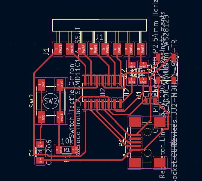
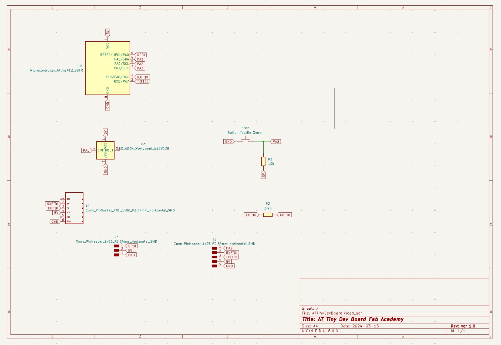
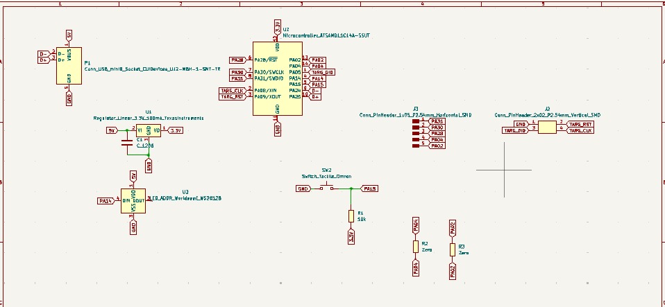
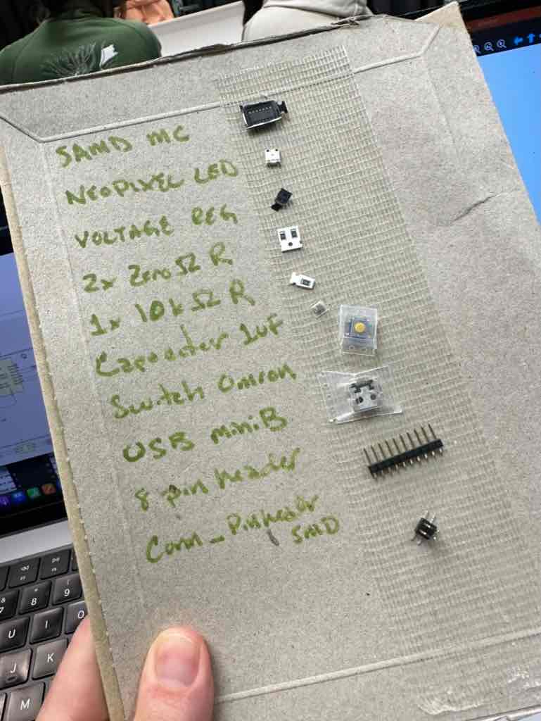
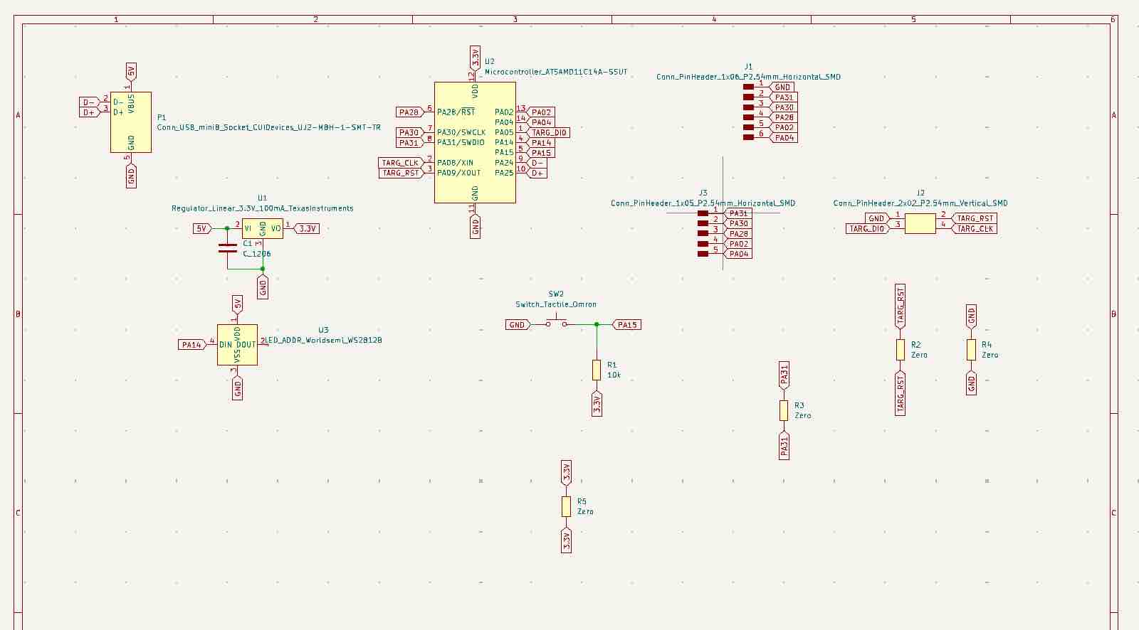
For the SAMD board, I used the following components:
- SAMD 11C - 14-pin microcontroller
- USB mini B for power and data input - Series UJ2-MBH-SMT
- A voltage regulator - this steps down voltage to the 3.3V required by the SAMD MC, whereas the USB input is 5V
- A Worldsemi Serial RGB LED
- A tactile switch (Omron) plus plus 10k resistor
- A pinheader with 5 pins to expose additional outputs
- At least 2 zero Ohm resistors for bridging copper traces
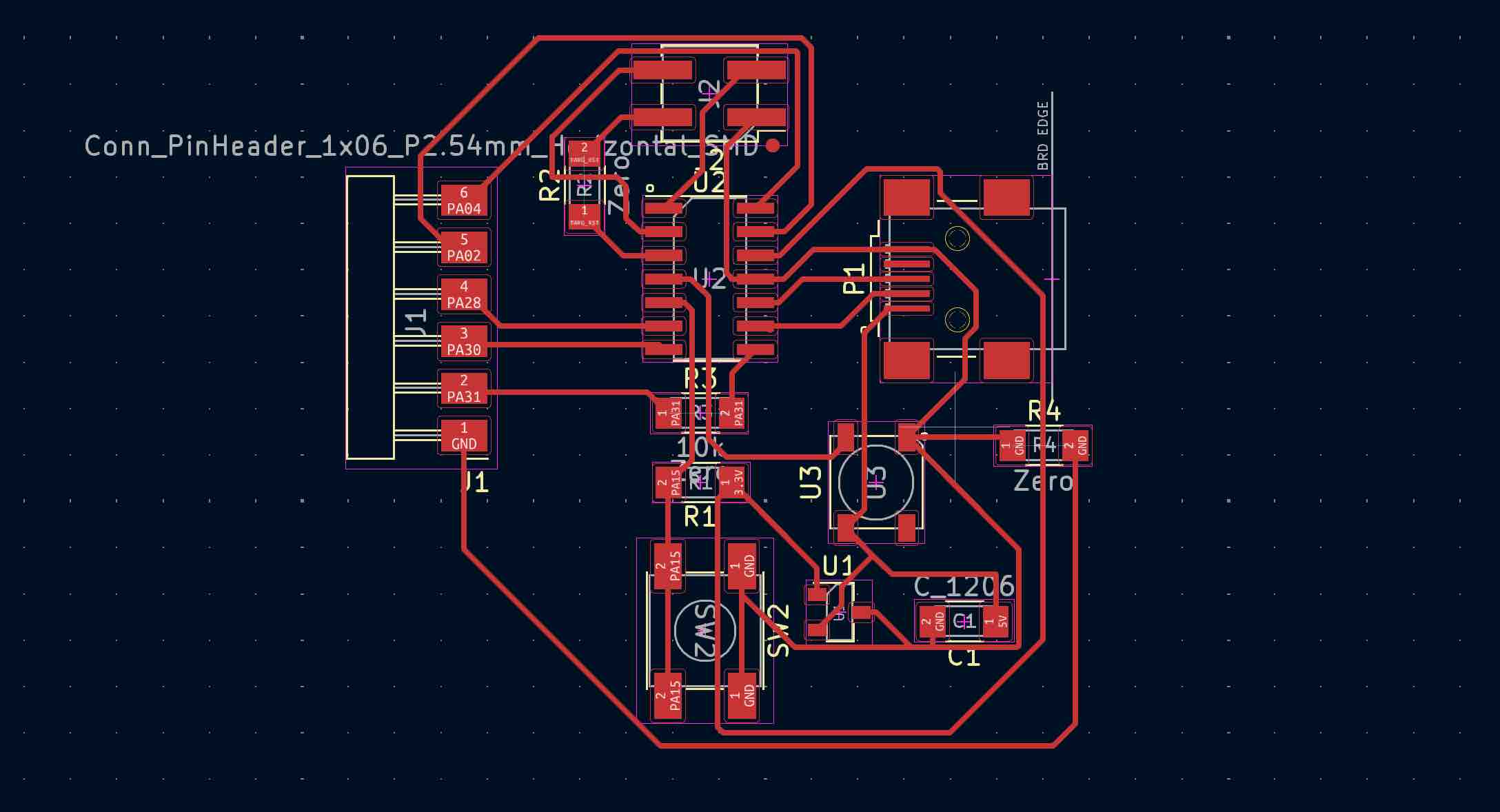
I created the design using Kicad, a program the allows you to select components for creating PCBs (such as those listed above), connect them using a schematic editor, and then draw the board layout including traces to be milled between the components.
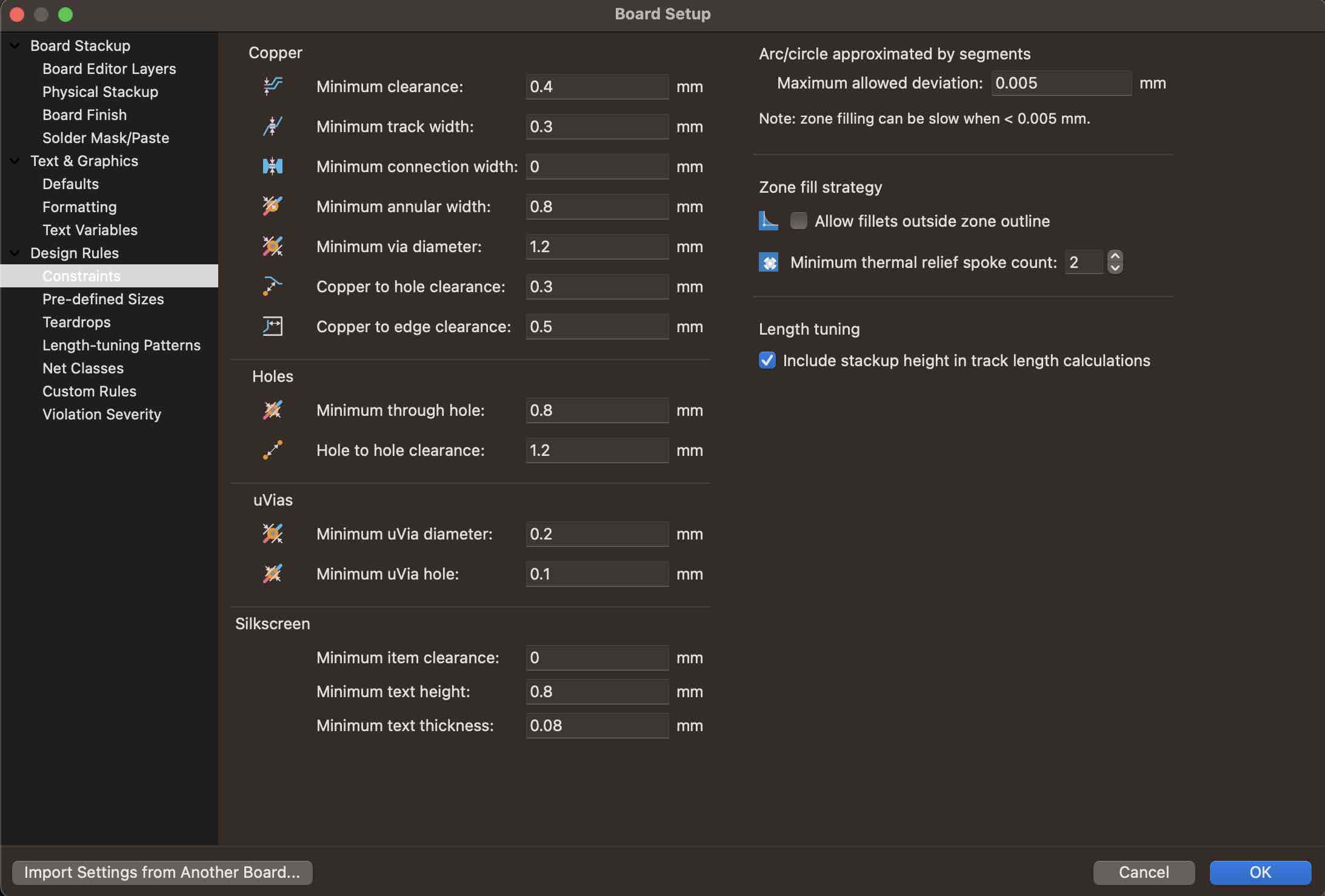
Before laying out the PCB we set design rules to ensure the appropriate clearance and sizing of components and traces. Most importantly we set the clearance to 0.4mm and track width to 0.3mm. Via size should be set to 1.2mm (this is the connectteion between layers - e.g. the copper left around holes) and the Via Hole to 0.8mm (diameter of drill hole).
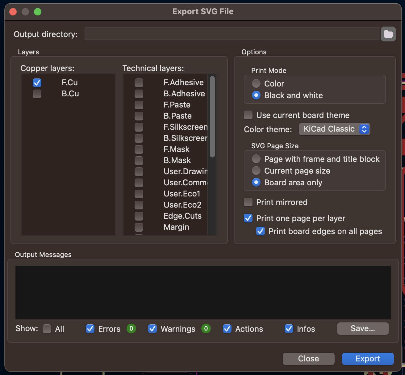
Once the PCB design is complete it needs to be exported and loaded as PNG files into mods to create the toolpath (just as we did in assignment 4). I exported from Kicad as an SVG (select "F.Cu" to export copper traces, make sure to select "print board edges on all pages" and print mode "black and white"). I then opened with Inkscape (you can use any vector image software) to create 3 PNG files: traces (copper paths and footprints on board), holes (drill holes on board), and outline (outline of board). To work correctly with mods, the traces need to be in white, with background in black. For holes png, the holes should be black with white or transparent background. For outline png, the outer area should be black and inner area (board area) white - the tool path will cut the border between the two. All settings used in mods and for the milling machine are the same as in assignment 4.
KICAD DESIGN RULES
KICAD EXPORT
SCHEMATIC
PCB
COMPONENTS
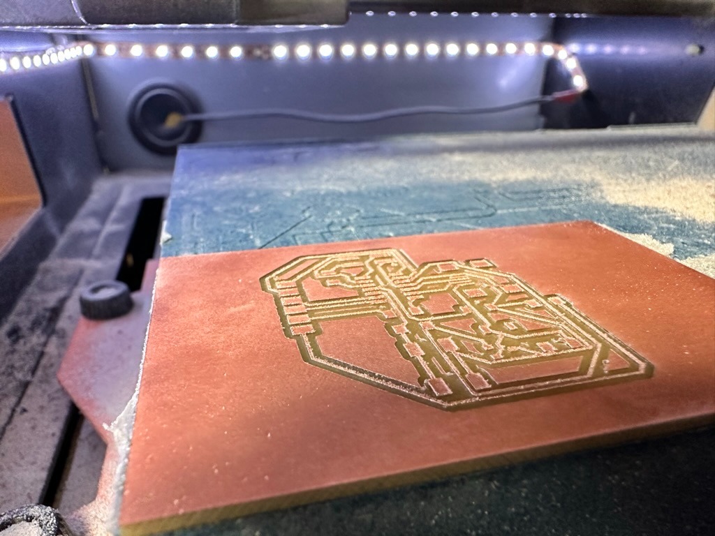
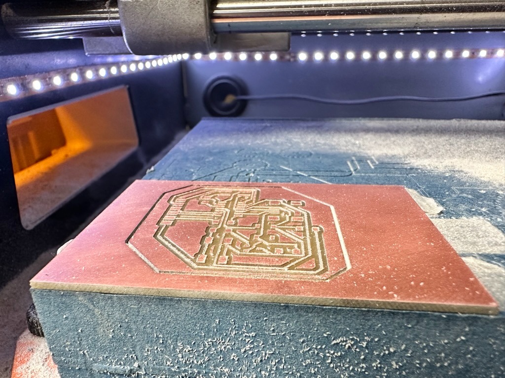
Final Board
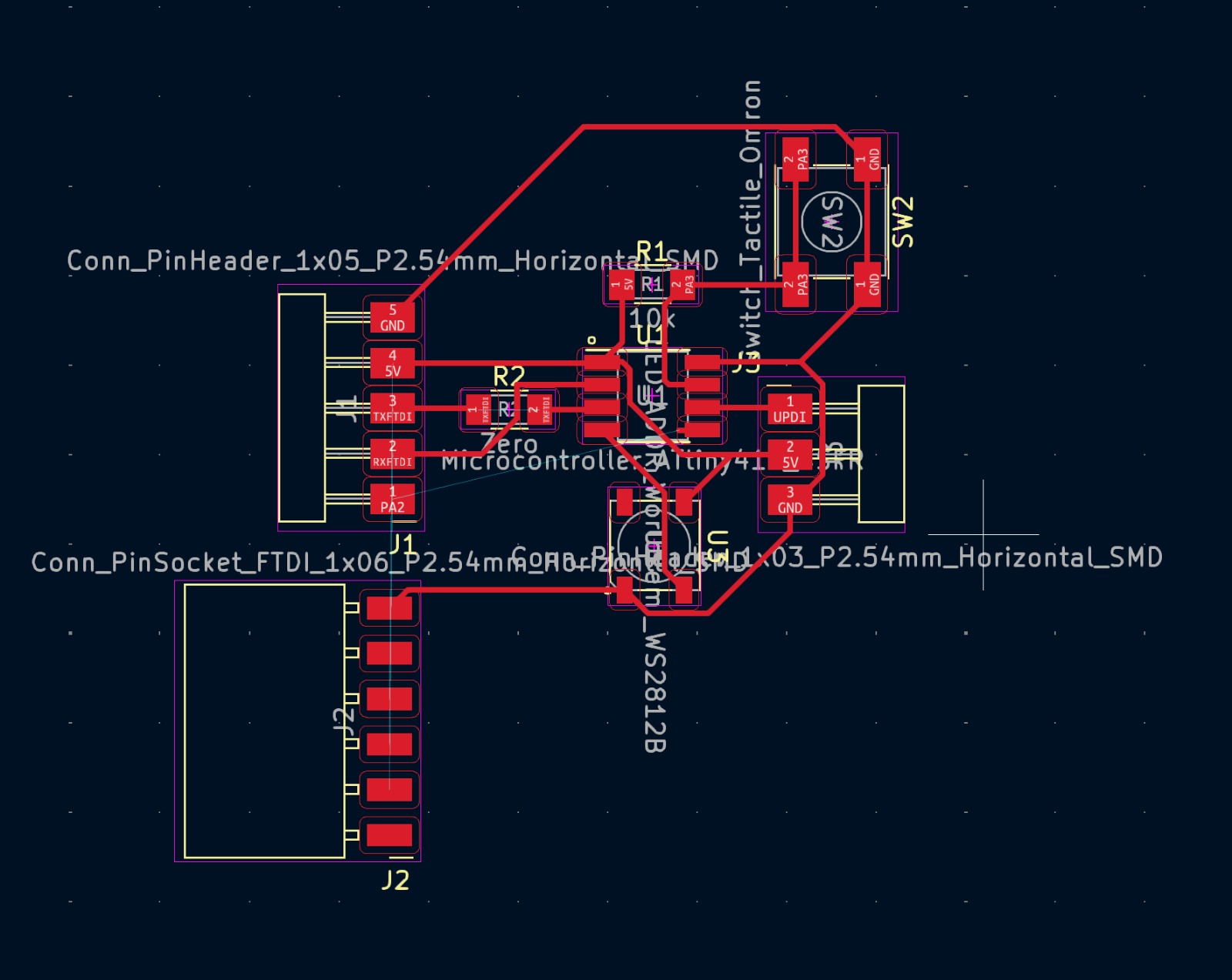
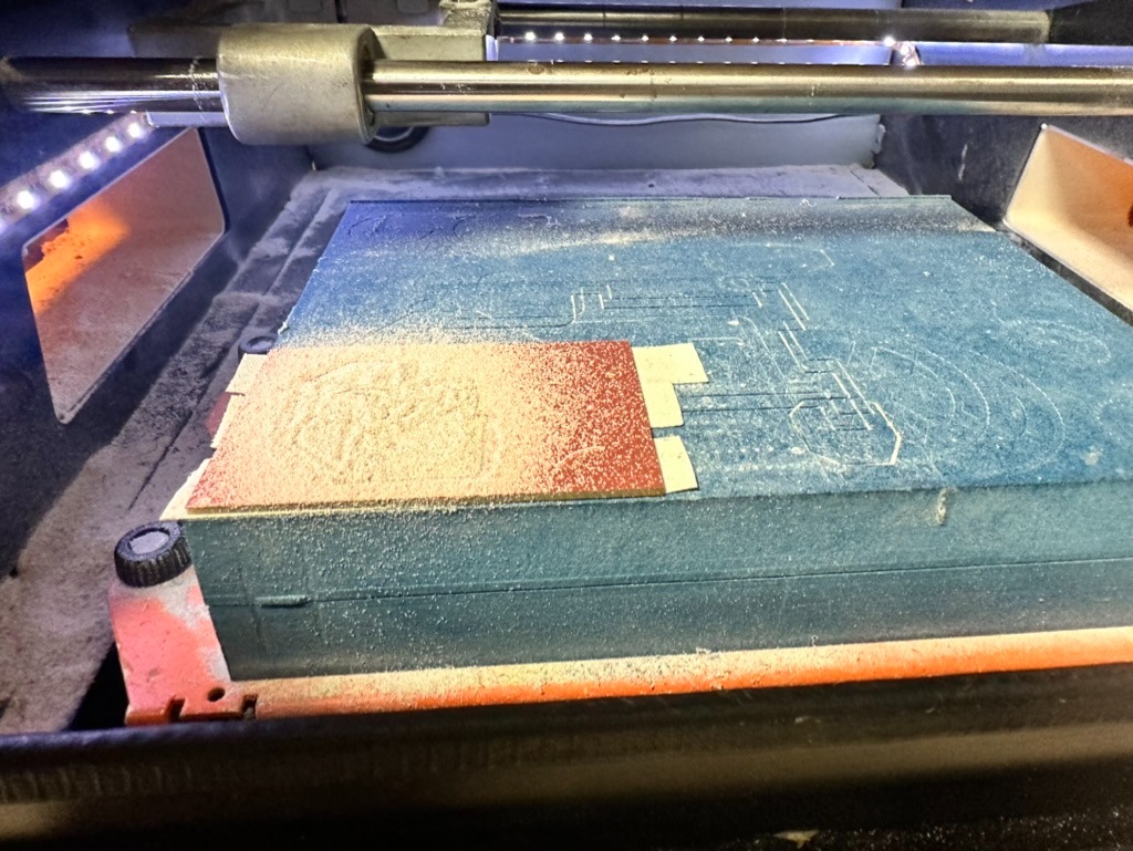
The board above was mostly correct, however the design above left out a ground pin. I therefore made a slight redesign to add this. I also had to cut the board 2x as some of the traces overlapped - e.g. the USB traces merged together. I stuffed and soldered the board.
RECUTTING BOARD
SCHEMATIC
PCB
Initializing and Testing my Dev Board
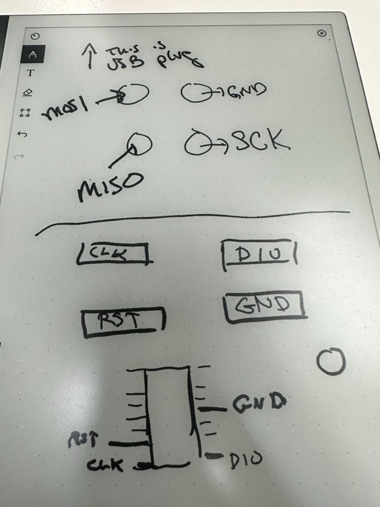
The first step was to get the bootloader onto the the SAMD11 using the Quentorres. This initializes the board; configuring pins and preparing it for programming. I plugged the SAMD board into the Quentorres and into a power source, and the Quentorres into my laptop. I mixed up the pin location so with the help of our teaching assistant Adai, I had to figure out which pins to connect between the Quentorres and my board: Ground, Reset, Digital I/O, and Clock.
I then downloaded the bootloader GET LINK and used the terminal to upload it. I had to play around with wires to get the connectivity right - especially with a Mac connectivity is very finnicky and sensitive (some cables work, some don't!). Finally I modified the button state program to work with my board.
BOOTLOADING FROM TERMINAL
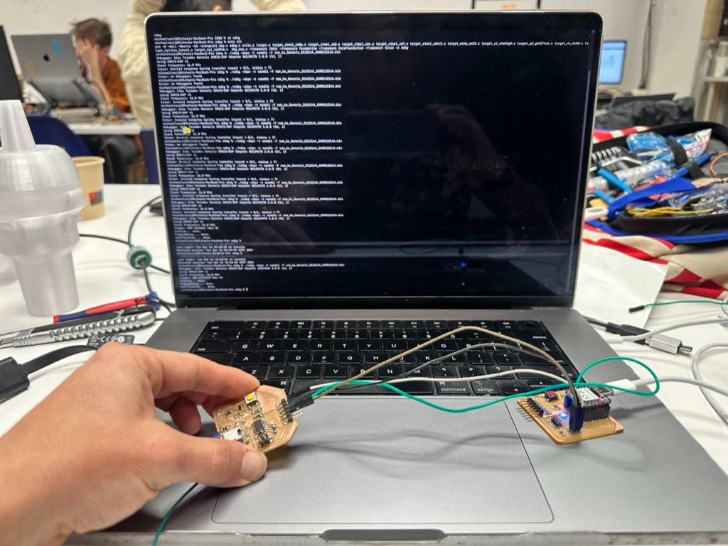
MATCHING PINS
BUTSTATE SOURCE CODE
int button = 15;

void setup() {
    // put your setup code here, to run once:
    //pinMode(D0, OUTPUT);
    pinMode(button, INPUT);
    Serial.begin(9600); //sets speed?
}

void loop() {
    // put your main code here, to run repeatedly:
    bool butState = digitalRead(button);
    Serial.println(butState);
    delay(500);
}
WORKING BOARD
Key Learnings
My main takeways from this week's work are:
- Think carefully upfront about what you need your board to do - it's more important that it can achieve its functional goals than having the smallest chip or the biggest chip or other meta or vanity requirements.
- Troubleshooting a board takes time - you should build a board that is going to last you a few test cycles if possible - e.g. ensure it has functionality beyond the minimum set required for your first tests.
- Design traces for easy soldering - no complex turns at soldering points, keep traces extra far if possible.
- There's nothing wrong with a larger board for a v1 - get smaller later.
Files
- SAMD Deb Board PCB
- SAMD Deb Board Schematic
- Final Board - RML Traces
- Final Board - RML Holes
- Final Board - RML Outline
Test Board - Group Work
The group work can be found here. We observed the operation of a microcontroller PCB using a multimeter and oscilliscope. The multimeter measures voltage changes across specific points whereas the oscilliscope can be used to visualize those voltage changes over time.