8. Electronics Design
This week we are working on developing a board that will connect the microcontroller to a ECS for a brushless motor, input slider/dial and a power source.
This is in preperation for the final project where I will have multiple motors for my electric spinner.
Design
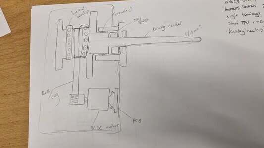
We mocked up an idea in the past to have the motors in the final machine be modular. Removable so you could just use one with an apropriate attachment. Possible applications:
Walking Wheel Spinning
This type of spinning seperates the the process of winding on and the twist of the fibers into two steps. This simplifies the process but involves the spinner walking forwards and back so it is more taxing.
The walking wheel has a large drive wheel which the spinner moves with their right hand clockwise whilst holding the roving in their left and walking backwards. This causes the fibers to be drawn out and a twist applied by having the created thread fall off the end of a needle.
The spinner then spin the wheel the other way to wind on the created thread.
First interation
For our first attempt at making a board for the final project we are making a cut down version using a stepper driver. We are likly to move to a brushless motor but the rpm needed for spinning is proving hard to find out. Our current estimate is 600-2000rpm range where a stepper motor is probably too slow.
PCB Design
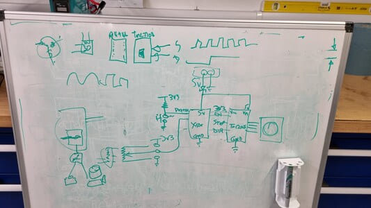
I have made some project in KiCAD previously, using the software seems relativly streight forward, however the electronic design side of it is daunting as there is a lot to consider.
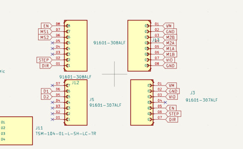
For the stepper driver we are going to use a TMC2208 SilentStepStick. This driver utalised the stealthchop mode for basically silent running of two phase stepper motors by automatically controlling the motos phase currents. This driver also features microstepping.
Looking at the TMC Pinout depending on how you want the device the function you can wire certain points to high (power) or low (ground).
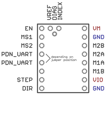
MS1 and MS2 set the step configuration. We are going to hard wire them so it turns in half steps. Therefore we need to wire MS1 to VIO (Logic Supply Voltage (3.3-5V)) and MS2 to GND. Stepper motors come in various step angles, with common values being 1.8 degrees per full step (200 steps per revolution) and 0.9 degrees per full step (400 steps per revolution) and give us a rough rpm of 125.
M1A, M1B, M2A, M2B are the motor coil inputs for the stepper motor. We will need to connect these to pinheaders.
STEP carries the signal from the microcontrolled to the driver that tells it how many steps to make.
DIR will give the signal to change the direction of the motor.
EN enables the motor output, GND=on, VIO=off. This could have been hardwired but we have connected this to a microcontroller pin so it can be controlled digitally.
Finally we have two power inputs. VM Motor Supply Voltage (5.5-35V) and VIO Logic Supply Voltage (3.3-5V) which need to be wired appropriatly.
Now for the XIAO pins.
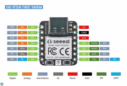
Following research last week we know the pins D0 - D3 on the XIAO are able to be used as interupts and wake the board. We will wire two inputs then using the D1 for a analogue input from a foot pedal and D2 for a push button. WE will need a pullup resistor for this button to stabalised the input signal. The botton will be soldered on, the analogue will use a 3pin header.
We will use D7, D8 and D9 for the EN, STEP and DIR outputs to the motor driver.
THe XIAO will take the input from the power source, through a diode, for the 5v. It will also produce the 3v3 for the driver pin VIO using its built in converter.
KiCAD
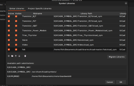
You can download KiCAD from here. I then installed the fabacademy footprint and symbol libraries. You do this my downloading the files and unzipping them within a folder where you can to put all your libraries.
Then in KiCAD to to preferences > Manage footprint libraries/Manage symbol libraries and create a new library for fab. The .pretty is the footprint file, the _sym is the symbol file.
There are many useful shortcuts in KiCAD, the bare minimum is 'M' to move, 'G' to drag and 'R' to rotate.
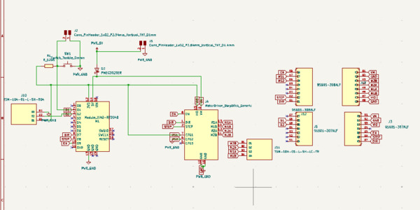
I started by using the component menu and finding all the components we decided to use in our design.
The only main issue was that the exact motor driver was not in the libraries but the 'Motor Driver StepStick Generic' was a good standin.
I used the wire tool to connect the pins together. For the grounds I just used multiple ground compnents. I could have also used global labels instead of wires for a cleaner layout but slightly harder to follow.
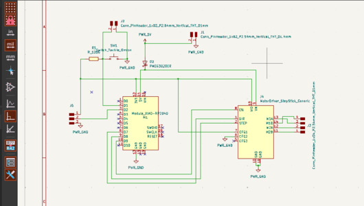
I used the 'Fill in schematic symbol reference designators' to make sure everything was labelled, more important when you have multiple of the same component.
Then we use the 'Run footprint assignment tool'. In my case the comonents had footprints assigned to the symbol, however you may need to choose what package any resistors or diodes are.
We can now go to the PCB editor.
PCB Editing
We first start by using 'Update PCB with changes from schematic'. This will import all the footprints all tangled in a rats nest.
Need to seperate the components so that the preview connections can reach their destinations.
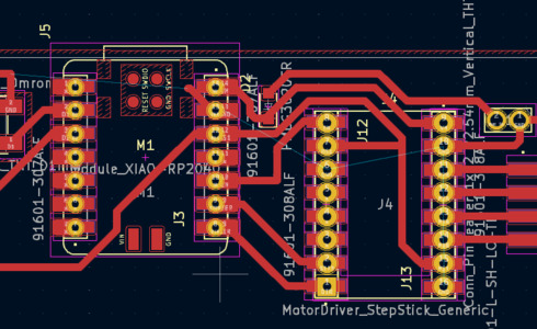
I also set a new track width of 0.8mm which I have found is a decently bulky trace which allows for some leeway when milling, but still not too large.
Layed out the components to that outputs were on one side, microcontroller in the center then outputs on the other.
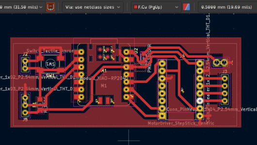
I then used the wire tool to connect the pads together. The groud pads should not need connecting as we will use a area fill for the ground plane.
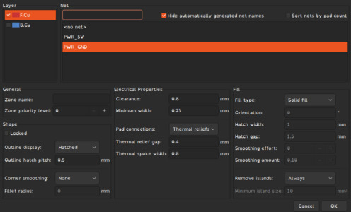
Use the fill tool to roughly draw around the board. Need to set it to be a PWR_GND fill and make sure its on the F_CU layer. You can edit the thermal relef spoke widths. I tend to increase their size to match the track width.
Issues
One of the problems which I had not come across before was the GND pads not automatically murgeing with the GND area. This may have been a issue with lack of space for the spokes but there seems to be enough space. To overcome this I just used a track that went into the GND area to bridge the gap.
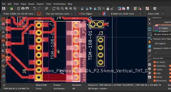
We printed off the PNG of the F_CU layer to test fit components. The revealed another issue. If we planned to use through-hole pin headders the tracks would not line up to the pins as the components will end up flipped to the other side of the board. We could solve this by flipping the components in the PCB editor and rerouting, however we decided to try out the SMD pin headers instead.
I did accidently add pin headers instead of pin sockets the first time round. I then connected this in version 3.
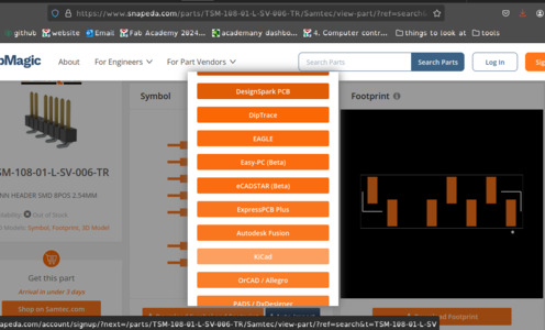
I found some components on RS which fit the requirements and were in stock. They also had footprints available on snapeda.
You download the zip file, unzip it in in your libraries folder then go through the process of adding the symbol and footprint though the kicads respective managers.
I edited the schematic to include the new sockets. I used global labels this time to help connect everything.
I imported into the PCB editor, overlayed the headers on the XIAO and motor driver then made sure the traces were connected.
I drew a outline on the edgecuts layer.
I used the 'Design rules checker' to double check the board. There were quite a few false alarms from where the unused pads overalapped or the silkscreen being covered. It did help me spot some of the ground pads not connecting like last time.
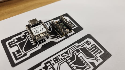
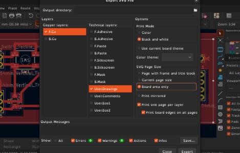
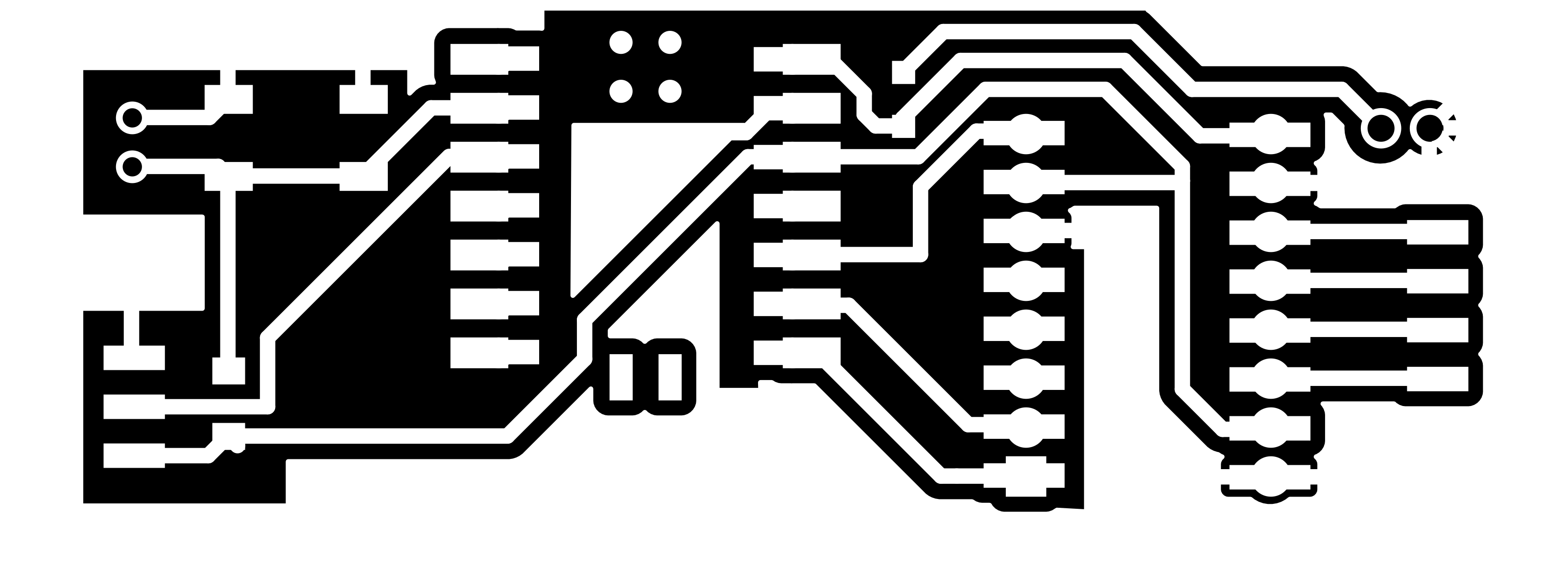
I then exported the F_CU and edge cut layers as SVGs.
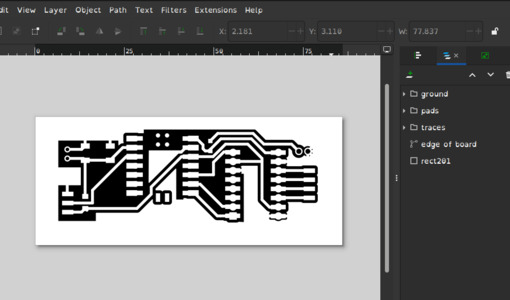
Inkscape
I opened the files in Inkscape. Looking in the objects you can see all the paths of the imported items, I went through and grouped together the pads, traces and ground objects.
I then resized the page to be about 6mm larger than the PCB then centered the design.
Depending on the object you either used a fill or just the outline to recolour the objects.
White is copper and will be preserved.
You can recolour the background of the page or/and use just a rectangle to fill in the background.
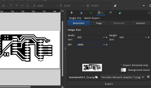
I then exported the PNGs at 1000 dpi.

Mods project
Using the Mods Project site we can generate a tool path for the milling. During Week 4 Electronics Production we explored the design settings for PCB milling and I used similar settings again. The main changes was that the offset overlap could be increased to 1 full diameter.
Traces
Cut/Holes
The milling took about 40 minutes to finish in total. The traces ended up quite deep, this is a common issue, I will need to run some tests in the future to determin the best height.
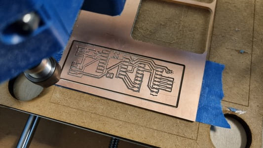
I did some deburring and then removed some of the extra copper islands that were left behind.
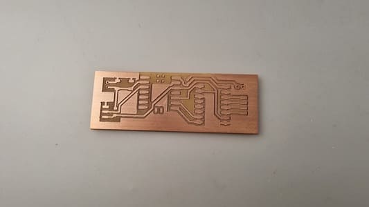
There was one issue that we will need to fix. The GND pin on the XIAO is not connected to the GND of the rest of the board. I will either bridge it using a 0 ohm resistor or drill holes and use a wire behind the board to join them together.
Soldering the Components
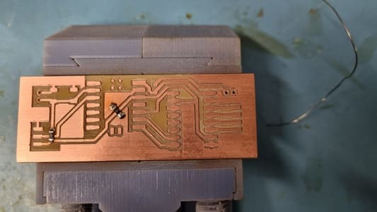
The first task was to bridge the two ground layers together using a 0 Ohm resistor. It is always a bit difficult to solder to the flat copper but it worked out decently this time.
I then soldered the other small components, the diode and the button, to the board.
I then soldered one of the 7 pin sockets to their pads. In order to get the correct distance i used the XIAO to hold the other socket in place whilst i tacked it down. I then removed the XIAO to minimise how much heat it experienced.
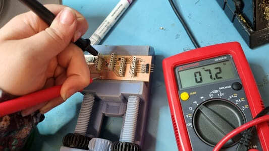
I then went round with the multimeter to check for any shorts.
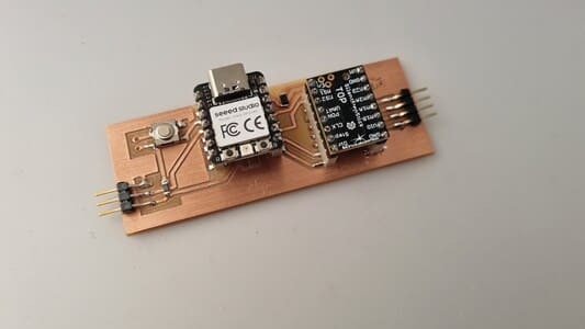
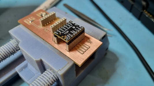
Here is the final board which we will code next week.
Here is a video of it working see week 9 for more details.