   group assignment:
      characterize the design rules for your in-house PCB production process
      extra credit: send a PCB out to a board house
   individual assignment:
      make and test the development board that you designed
         to interact and communicate with an embedded microcontroller
      extra credit: make it with another process
Group work
This week was our college's spring break. As a faculty member on sabbatical, I spent the week working (mostly on week 7 stuff), but most of the students were out of town, so I wrote up the group work individually below.Our lab has a Roland SRM-20 and a Sainsmart Genmitsu 3018-PROVer. I'll be producing my board on the Sainsmart, but we focused on the Roland in the lab activity. They use the same cutting bits, and their capabilities and design rules are very similar.
The Roland has the following major design limitations:
- Our standard bit for cutting traces is 1/64" (0.4 mm) in diameter. This means it can't cut inside or between features less than 0.4 mm apart. We do have some smaller bits (including a 1/100" bit), but these are not recommended for beginners.
- We will be cutting 1-ounce single-sided FR-1 PCB board. The copper layer on this is about 1/1000 inch (0.03 mm) thick. Traces need to be wider than they are thick to avoid peeling off the substrate, so traces smaller than a few thousandths thick are likely to be problematic.
- The Roland has a horizontal workspace of 203 x 152 mm, so we can't make a board bigger than that.
- The FR-1 board we have in the shop is 6 x 4 in. (152.4 x 101.6 mm), which is the real limit on the size of PCB board we can make.
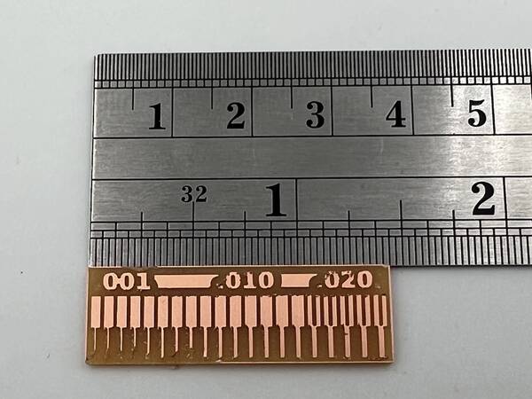
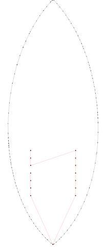
The first picture below is a test file we were provided, intended to demonstrate the limits of our machine. The second picture shows the actual board milled by the Roland.

How these limits informed my design process
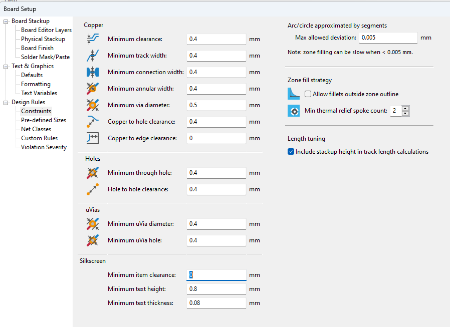
For my board, in KiCAD I made all traces at least 0.4 mm wide, doubling that to 0.8 mm when practical. I set all clearances between anything and everything else to 0.4 mm.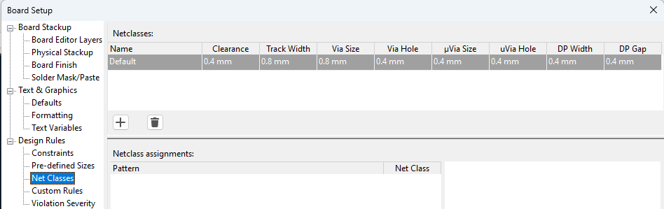
Design Work
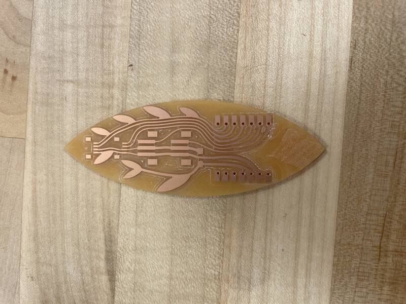
As mentioned in Week 6, my plan is to create a development board based on the Seeed Studio Xiao boards, that interfaces with sensors and I/O devices using the STEMMA and Qwiic plug-and-play microcontroller systems offered by Adafruit and Sparkfun. Since it's a Qwiic Stemma that starts from a Seeed, I call it "Beansprout".
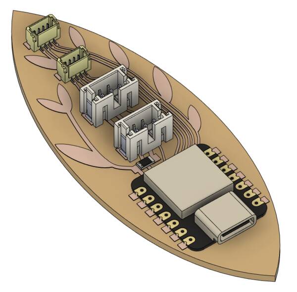
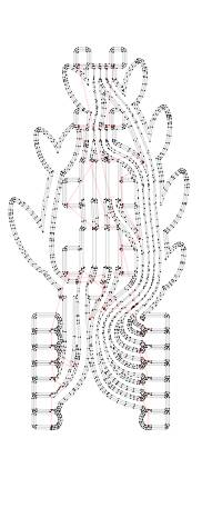
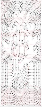
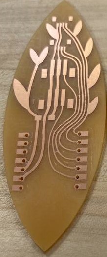
I wanted to lean in to the "beansprout" idea with some plantlike aesthetics for this, so I took my finished KiCAD design and imported it as an SVG into Adobe Illustrator. I deleted the angular traces KiCAD creates and replaced them with organic tendril shapes, and added decorative "leaves". I also designed the board outline to have a lenticular "leaf" or "pod" shape. Boards I create in later weeks will have the same shape, and will connect to the dev board with cables in daisy-chain fashion to create a leafy vine. Here's my final design: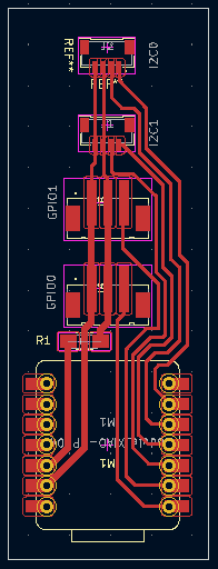


The leaves are cosmetic, but they can serve a purpose. One could clip a multimeter or oscilloscope to the leaves on the left side to get a +3.3V or GND reference, or touch a probe to the right-hand leaves to get the SCL0 signal, which I guess isn't so useful.
And it was at this stage, going from KiCAD to Illustrator, that I made a critical error that I only discovered while writing the previous sentence. Can you spot it in the images above? I'll get back to it.
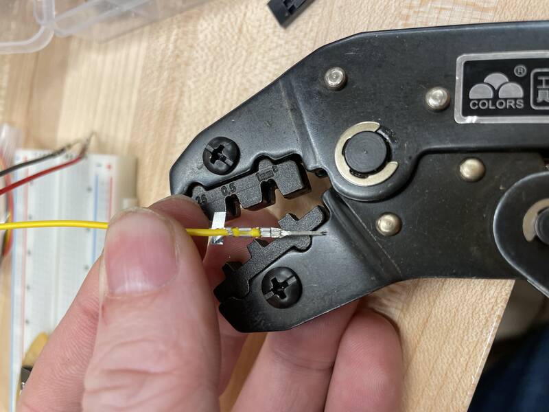
To get ready for this week, I also asked my instructor to order the JST-PH and JST-SH connectors I would need for this board, plus a bunch of Qwiic and Stemma cables, and a JST connector crimping kit so I can make my own if I need to.
3-D visualization
Since the aesthetics of this design are pretty important, I wanted to get a good look at a 3-d model of the finished board. KiCAD can help you do this, but since the board was designed with both KiCAD and Illustrator, I used Fusion 360 to get a final image. My steps were as follows:
- In KiCAD's PCB Editor, I chose View / 3D Viewer. The view was disappointing, because KiCAD doesn't have 3D models for any of my components.
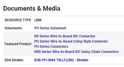
- I found each part on Digi-Key's website. On the part page, there's a Documents and Media section with a link to the "EDA Model" for the part. Usually this will take you to a page with links to a site like SnapEDA to download a STEP model for the part. Sometimes you might have to search these sites manually. I downloaded:
- BM04B-SRSS-TB(LF)(SN) from SnapEDA
- B3B-PH-SM4-TB(LF)(SN) from SnapEDA
- Seeeduino Xiao from GrabCAD
- I put these files in the fab.3dshapes folder in the Fab Academy KiCAD library.
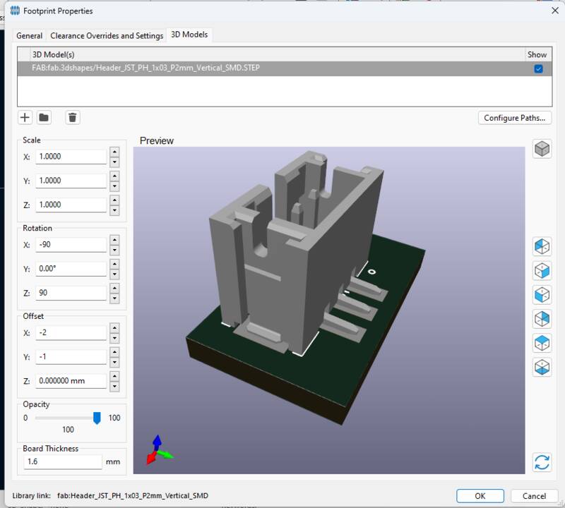
- In the KiCAD footprint editor, I right-clicked on each footprint, chose "Properties" and selected the "3D Models" tab.
- I added the 3d file in the top panel, then adjusted the rotation and position of the model so it was aligned with the pads in the 3D image.
- Once this was done for all components that don't have 3D models, I chose File / Export / Export as STEP file.
- Next, I opened the STEP file in Fusion 360. It doesn't have the pretty traces and board outline I made in Illustrator.
- I created a new sketch and imported the SVG files I created in Illustrator. As I found in Week 07, Fusion makes these the wrong size (I think Illustrator uses a different units-per-inch convention for its SVGs than other design tools.) Resize and move them to align with the parts in the STEP file.
- I extruded the board outline and the traces.
- Finally, I used Fusion's "Appearance" panel to make the board tan and the traces copper colored.
Preparations
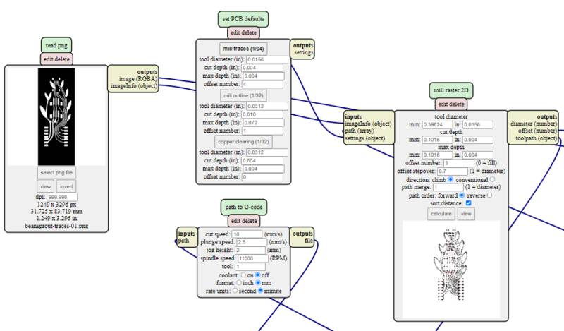
I prepared my file for machining in MIT MODS. I'll be using the Sainsmart mill for this, which does require a few steps of extra setup. I followed the steps in Wheaton's SainSmart Mill documentation, with a few changes.- Save your SVG files as PNG files at a resolution of 1000 DPI. I tried cutting from SVG files directly and had lots of problems, PNG worked better.
- In your web browser, go to https://mods.cba.mit.edu.
- First, we need to tweak MODS to support the Sainsmart mill. This only needs to be done once, and will create a new "local program" for Sainsmart PCB milling on your computer. If you've done this before, skip to Step 3.
- Right-click and choose "programs", "open server program", then choose "G-code: mill 2D PCB png".
- Click the “edit” button on the “Path to G-code” module.
- Delete the line
str += "T"+tool+"M06\n" // tool selection, tool change - Change the line
str += "G04 P1000\n" // give spindle 1 second to spin up
tostr += "G04 P1\n" // give spindle 1 second to spin up
The Sainsmart mill's delay times are in seconds, not milliseconds, and you don't want to wait 1000 seconds for it to start up! - Click "Update and close".
- Right-click and choose "programs", "save local program". A text box will appear in the upper left of the screen by the MODS icon: choose a good filename, like "sainsmart_2d_pcb_svg.txt". Hit Enter, and the MODS program will be downloaded to your computer.
- Next, right-click and load the local program you created above into mods.
- Select "Load PNG file" on the right panel, and choose your traces file.
- If your image is black-on-white, hit "Invert" to make it white-on-black. Black means "cut", white means "keep".
- Select "mill traces 1/64". I changed "offset number" to 3, and "offset stepover" to 0.7. This will make the cutting around the traces slightly wider in spacing, with fewer cuts, which should speed things up a bit. I also set "speed" to 10 mm/s, which was maybe a bit too fast.
- Click "Calculate" in "mill raster 2d". I inspected the 3-d view of the traces to make sure they were cutting the right thing. This downloads a .nc file that will be used to control the mill.
- I want a pretty board with all the copper removed except for the traces and leaves, so I repeated this process, choosing "copper clearing 1/32" as the cut profile.
- Finally, I repeated the process with the "outline" file that describes the board edges and through holes. This file also needs to be inverted to work.
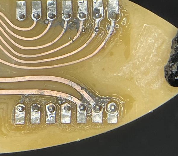
- I ran into a problem with the board outline: the fab library's Seeed Xiao footprint specifies 0.8 mm through holes. But since my cutting bit is also 0.8 mm, MODS can't create a toolpath for them, and refuses to drill the holes. So I went back in Illustrator and made the holes just sliiightly larger. I also changed the footprint file in KiCAD to have 0.81 mm holes, so I won't have this problem next time.
At the end of this process, I had created three files: beansprout-traces.png.nc, my machining file for isolating the traces; beansprout-traces-clear.png.nc, the file to clear the rest of the coppper from the board; and beansprout-outline-holes.png.nc, which cuts out the holes and the outline of the board.
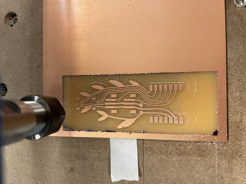
Machining
Once the .nc files are created, it's time to machine the board. The process is as follows:- Copy the traces, clear, and outline .nc files onto the computer that controls the Sainsmart.
- Attach a piece of FR-1 printed circuit board onto the spoilboard of the Sainsmart mill with double-stick tape. More so than with large-format CNC, it's crucial to get the tape even and smooth with no bumps.
- Turn on the Sainsmart (switch is on the back control board).
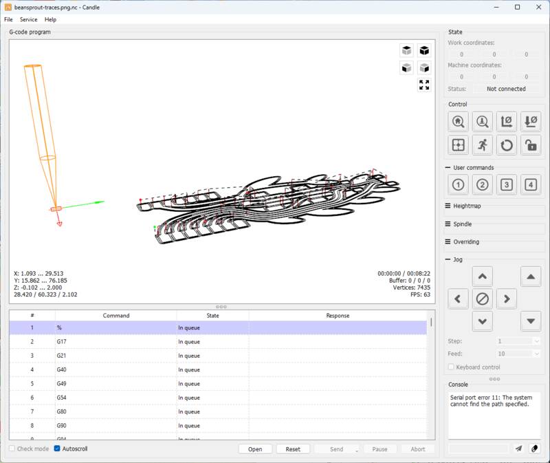
- Start Candle, the CNC control software, on the PC.
- in Candle settings, make sure the Sainsmart is connected via the serial port. Hit the "unlock" button, then check to make sure the status is "Idle". Hit the jog buttons (scroll down on the right panel if you don't see them) and make sure the cutting head moves.
- Load a 1/64" tapered stub bit into the collet. The Sainsmart's collet works the same as the Axiom's from Week 6, just smaller.
- Open the traces file in Candle. Candle will show you a 3D view of where it thinks the cutting bit is now, and where the design will be cut. Jog the bit to where you want the X,Y=0,0 position to be and hit the "XY Zero" button.
- Now set the Z-zero. The Sainsmart has a zeroing puck like the Axiom, but it doesn't always work and some parts were missing, so I did it by hand: I slowly lowered the bit toward the work, with a thin slip of paper between the bit and the board. Once the bit snagged on the board, I moved the cutting head down further by the thickness of the paper. I tried to be conservative, to avoid cutting too deep and breaking the bit.
- Click "Send" to send the job to the Sainsmart: it should start cutting immediately.
- Once the traces are isolated, switch to the 1/32" flat endmill and re-do the Z-zero. Do not re-do the X,Y zero.
- Cut the "clearing" and then the "outline" file with the 1/32" bit.
- You should be able to pry the board out of the PCB blank, leaving the rest for the next person.
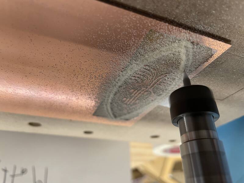
Look at that! I got it right on the first try! Go me! ... or so I thought, until I was doing documentation this morning and noticed a critical error. When I re-drew the traces in Illustrator, I drew them in the wrong positions! The right-side traces should connect to the second through seventh pins on the Xiao, not the frist through sixth! The whole point of software like KiCAD is to prevent mistakes like this, and by going through Illustrator I created a mess for myself.
So I had to re-cut the whole board all over again. And this time, it didn't go smoothly. In re-routing the traces, I put a few of them too close together so they didn't cut correctly, and then in moving them to make room I moved an entire trace instead of just part of it, causing another set of traces to fail to cut properly. The PCB blank had a strong bow to it, which I thought I'd solved with liberal application of double-stick tape, but the bow was more pronounced during the second cut. I broke a bit, then had to cautiously inch the z-zero downward a twentieth of a millimeter at a time until the traces were cut. And then I had to do it again for the clearing step. And even then some copper was left on the board, which I scraped off by hand afterward.
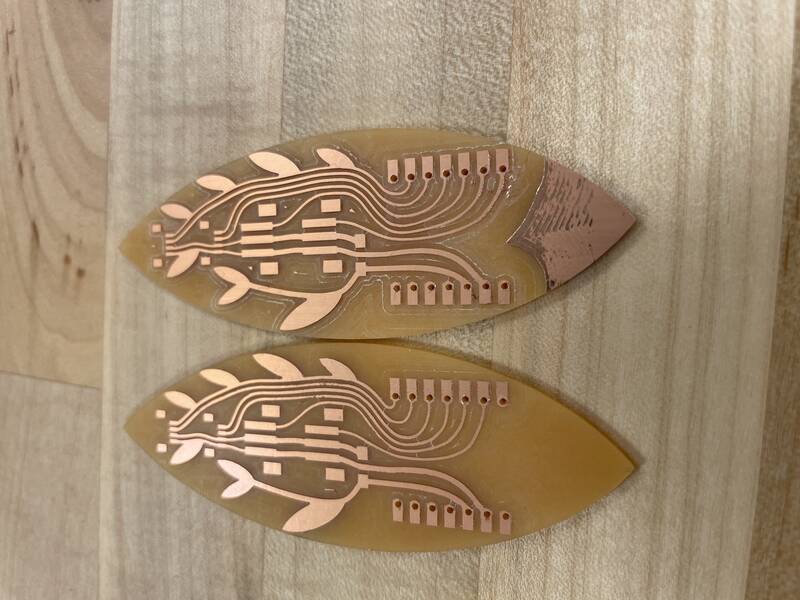
But in the end I got it done. Here's a comparison of my first and second versions, showing both the corrected trace routing, and the much poorer quality of the second board.
Soldering

Next it was time to solder the components to the board. As mentioned in Week 6, I want to be able to have the Xiao both surface-mounted to my PCB, and also optionally connected to a breadboard with through-hole pins. If you don't like header pins you can just leave them out.
I used solder paste, but I wasn't able to use a hot air gun because the JST connectors were so large and lightweight that they blew away in the airstream. So I used a hand soldering wand to melt the paste.
I tested for continuity as I went for the first few parts, then as I got more confident I just went for it and soldered everything. This was a mistake. When I tested for continuity at the end, the 3V3, GND, and D10 pins were shorted together, as were SDA0 and SCL0. And since many parts shared these signals, there was no way to know where the soldering error was, so I had to completely un-solder the whole thing. Many of the parts were easily removed by holding the part with tweezers with the board hanging under it and hitting it with the hot air gun. But un-soldering the Xiao was really difficult: it's too big to heat all at once, it is itselfmade of soldered components and I didn't want to melt those, and the presence of solder in, under, and around the through-hole pins made this a huge chore. My clever "surface mount and through-hole in one big solder glob" idea really did not pay off.
Anyway, I re-soldered everything again, being careful not to over-apply the paste, and testing continuity after every part was added. And this time, finally, it passed the continuity test.
Testing
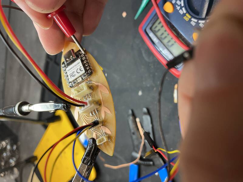
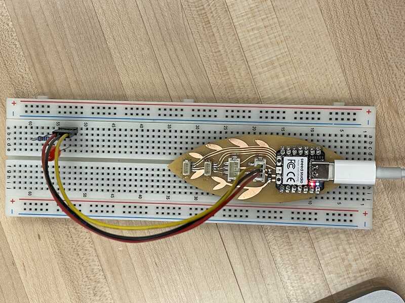
To test that the board was working, I used the cable-crimping kit I ordered to create a 3-pin Stemma to 3-pin Dupont header cable. I plugged one end into a GPIO socket on the Beansprout, and the other into a breadboard. I set up a 220-ohm resistor and an LED on the breadboard, and wrote a Blink sketch to run on the Seeed Xiao RP2040. And it works!Hero Shots
We're all going to have to agree to not talk about the quality of the soldering job here.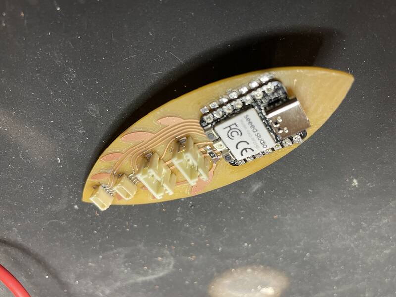
Design Files
- beansprout-v2.zip contains a STEP file of the 3-d model of the Beansprout board.
- beansprout-traces.png MODS-ready PNG file showing traces.
- beansprout-outline-holes.png MODS-ready PNG file showing board outline and holes.
- beansprout.ai Beansprout outline and traces file in Adobe Illustrator.
- sainsmart-pcb-png.txt MODS program to cut PCBs on the Sainsmart Genmitsu 3018-ProVer.