group project:
        use the test equipment in your lab to observe the operation
           of a microcontroller circuit board
     individual project:
        design a development board to interact and communicate
           with an embedded microcontroller
        extra credit: try another design workflow
        extra credit: make a case for it
        extra credit: simulate its operation
Regarding the group work, as a physics professor I actually have more experience using an oscilloscope than our class instructor, so he asked me to take the lead in teaching that side of the group lab activity. I have written up my lesson plans for what I showed the other students, in lieu of doing a group writeup myself. My instructor and I agreed that that was probably more useful to everyone than for me to join one of the groups.
Group Contribution: Oscilloscope Lesson Plan
This section describes how I taught the other students in my lab to use the Rigol DS1102E oscilloscopes in our Fab Lab. Other materials needed for the lesson: an Arduino and a computer to connect it to. (We used a Seeed Xiao ESP32C in the lab this week.)
- First, describe the purpose of the scope: to measure voltage changes that happen too fast to be detected by a multimeter or noticed by the human eye. The multimeter is great for basic problems -- is it connected? Does it have power? while the oscilloscope is great for debugging complicated circuit problems -- is the microcontroller sending data as it should? Is there electrical interference causing trouble?
- Now show the basic controls, and how to hook up the probe:
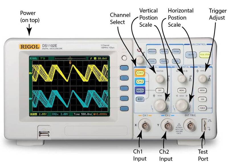
Basic controls for the Rigol DS1102E oscilloscope. 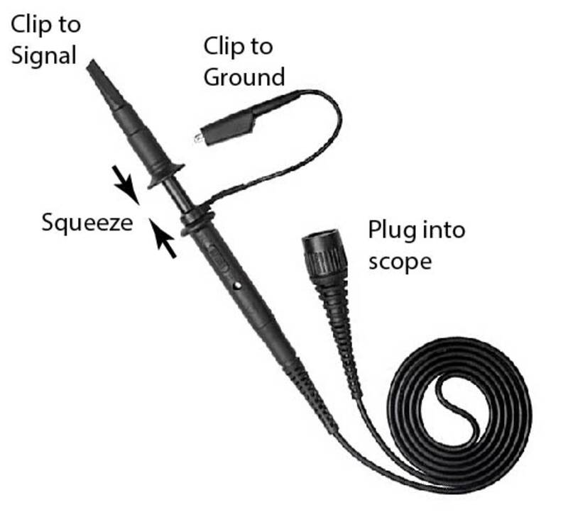
How to connect the probe to a circuit. - To demonstrate the concept, program an Arduino Uno with the standard
Blinksketch. Attach the oscilloscope to ground and to the LED pin. Set the vertical scale to 1V/division, and the horizontal scale to 0.5 sec/division. Students will be able to see the trace slowly moving across the screen illustrating what the scope does, at human-eye speed. - Now ask students to modify the
Blinksketch with a much shorter delay (say, 1 ms instead of 1000) and tune in the scope to find the signal. Demonstrate the following:- Adjust the horizontal scale for the new pulse frequency
- Adjust the vertical scale
- discuss the scale of the grid lines on the screen and how to read them quantitatively (each square is one of the divisions selected on the scale knobs.)
- Show how the "trigger" knob can be adjusted to synchronize the oscilloscope with the input signal, and how hard it is to read when the triggering is too high or low
- Demonstrate pulse width modulation, and how it works, using the following code:
Students can see that "Analog" output varies the duty cycle of digital pulses.
int ledPin = D8; void setup() { // initialize digital pin ledPin as an output. pinMode(ledPin, OUTPUT); } void loop() { analogWrite(ledPin, 100); // Turn the LED on weakly delay(1000); // wait for a second analogWrite(ledPin, 200); // turn the LED on brighter delay(1000); // wait for a second } - Finally, we can show how the "bits" of binary communication work. The following code creates a serial output on the same pin that was being used for blinking earlier, so we can see the direct binary signals the chip emits as it sends "Hello World.":
HardwareSerial MySerial(0);

void setup() {
  // Initialize custom hardware serial port
  MySerial.begin(9600,SERIAL_8N1,7,8);
}

void loop() {
  // put your main code here, to run repeatedly:
  MySerial.write("Hello World"\n);
  delay(50);
}
I wrapped up the session by talking in general about some of the advanced features of the oscilloscope so students know what's possible and can look up the details:
- capturing "one-shot" traces rather than a continuous sweep
- analyzing frequency and amplitude of signals
- showing two signals at once
- using the "test port" to make sure the scope is set correctly
- saving trace data to a USB flash drive
Development Board Design
For my indivdual project, I designed a development board using KiCAD. I have some experience doing circuit board design already, so I took this as an opportunity to do something more aesthetic and not just utilitarian.My concept is called "Beansprout", and the goal is to allow the Xiao Seeed processors to interface with the quick-connect Stemma QT and Qwiic cabling systems by Adafruit and Sparkfun. (It's called Beansprout because it's a Qwiic Stemma that starts from a Seeed.)

Design goals are as follows:
- Provide two separate I2C interfaces using 4-pin JST SH connectors (1-mm pin pitch) that match the Stemma QT interface. Cable pinout:
- GND
- +V
- I2C SDA
- I2C SCL
- Provide two general-purpose analog/digital input/output sockets (GPIO) that match the Stemma interface: 3-pin JST-PH connectors (2-mm pin pitch) that match the Stemma interface. Pinout:
- GND
- +V
- Signal
- Expose all other pins to the outside world using a common 0.1" header, so you can plug into them like an Arduino Uno.

I took a lot of notes while planning this out, including links to components, a tangent about selecting magnetic field sensors for the final project, and the details of the Stemma system. Most of this is captured in the page you're looking at now or my final project page, but for the sake of completeness here's a link to my Google Docs notes.
KiCAD Concepts and Glossary
There's a lot of new concepts and terminology in circuit board design, so here's a quick definition of terms and ideas:- Schematic: A diagram of the conceptual layout of your circuits. This shows what must connect to what, but not how that connection will be made physically. Parts are represented as black boxes, rather than their physical appearance.
- PCB: A diagram of the physical appearance of copper traces on your circuit board. This shows how the connections described in the schematic will be made physically. Parts are represented by their "footprints".
- Symbol: The "black box" representation of a part in the schematic editor.
- Footprint: The solderable connections that must be made to connect to a part.
- Trace or Track:The copper path on the PCB that connects parts together.
- Design Rules:The clearances, widths, and other limits that must be followed to make sure a board can actually be manufactured with a given set of tools.
- Net:A set of traces that are all physically connected together and should be at the same voltage.
- Pad: a solderable piece of copper that provides a mounting point for one of a component's pins.
Installation and Setup
I followed our instructor Brandon's procedure for setting up KiCAD for FAB use.- Download KiCAD from https://www.kicad.org/download/windows/.
- Install the Fab Academy KiCAD libraries, which provide symbols and footprints for parts we typically have in the lab. To do this:
- Clone the Fab Library git repo. In git bash, do
git clone git@gitlab.fabcloud.org:pub/libraries/electronics/kicad.gitin the directory where you want the libraries to live. - Open Preferences → Manage Symbol Libraries. When prompted on first setup, choose "Copy global default symbol library".
- Click + to add a new library.
- Click the folder icon in the "Library Path" column, and find the fab.kicad_sym file in the cloned Fab repo. Choose the nickname "fab".
- Open Preferences → Manage Footprint Libraries. When prompted on first setup, choose "Copy global default footprint library".
- Click + to add a new library.
- Click the folder icon in the "Library Path" column, and find the fab.pretty folder in the cloned Fab repo. Choose the nickname "fab".
- Open Preferences → Configure Paths…
- Click + to add a new path that points to the git-cloned folder. Set the Variable Name to FAB.
- Clone the Fab Library git repo. In git bash, do
Creating a Board: First Draft, "Phat"
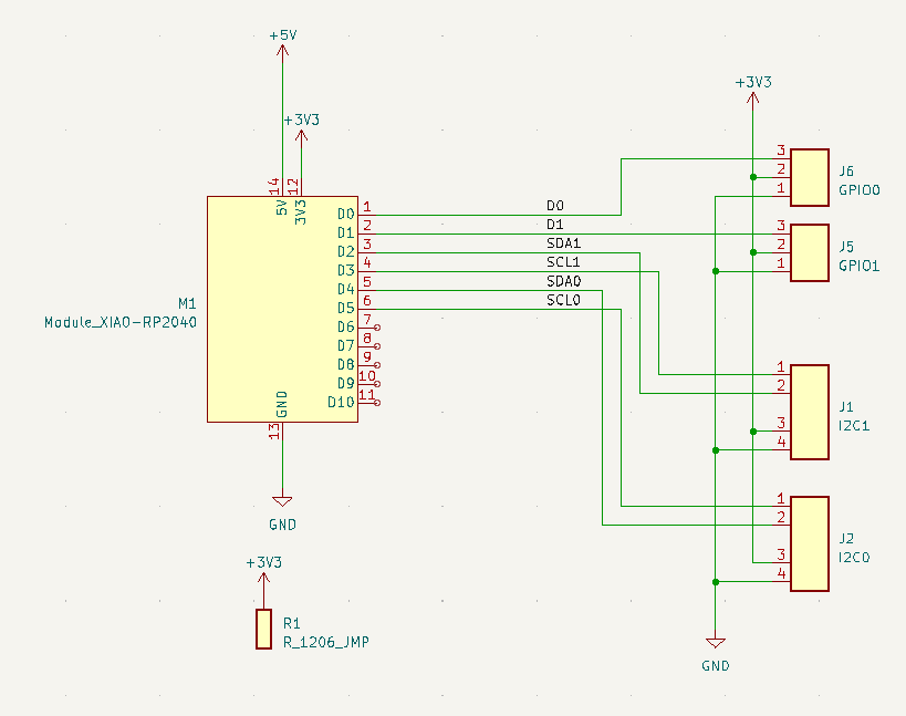
My first draft for a dev board, I just threw some parts together and hooked them up. The process is as follows. First, create a new project and open the Schematic Editor.Schematic Editor
- Add parts using the
 Add a Symbol tool to lay down my microcontroller and connectors. I used the following parts:
Seeed Xiao RP2040Conn_Header_JST_SH_1x04_Vertical_SMDx2 (Stemma QT I2C)Conn_Header_JST_PH_1x03_Vertical_SMDx2 (Stemma GPIO)Conn_PinHeader_1x07_P2.54mm_Vertical_THT_D1mm x2
(These are standard 0.1 inch header modules, like you find on an Arduino Uno.)
The 1x07 pin headers are through-hole mount, which isn't Fab preferred, but I couldn't find surface mount components. I plan to change them out later.
- Move the symbols around to make logical sense. You can pick them up to move with the "M" key, rotate them with the "R" key, and flip them horizontally and vertically with "X" and "Y".
- Add Power symbols using the
 Add Power Symbol tool. These have the special property that they're automatically wired up to each other: all GND symbols will be joined with traces on the board, you don't have to wire them up in the schematic. I used the following power symbols:
GND,+5V, and+3v3to match the power available from the Xiao. - Draw wires to connect the Xiao to the connectors using the
 Add a Wire tool. (Not the
  Add a Bus tool!)
 - Add Labels to the different signal lines using the
 Add a Net Label tool to indicate their function.
 - Add names to the different connectors to shorten them and indicate their function. Double-click on the symbol and change its "Value" to something meaningful.
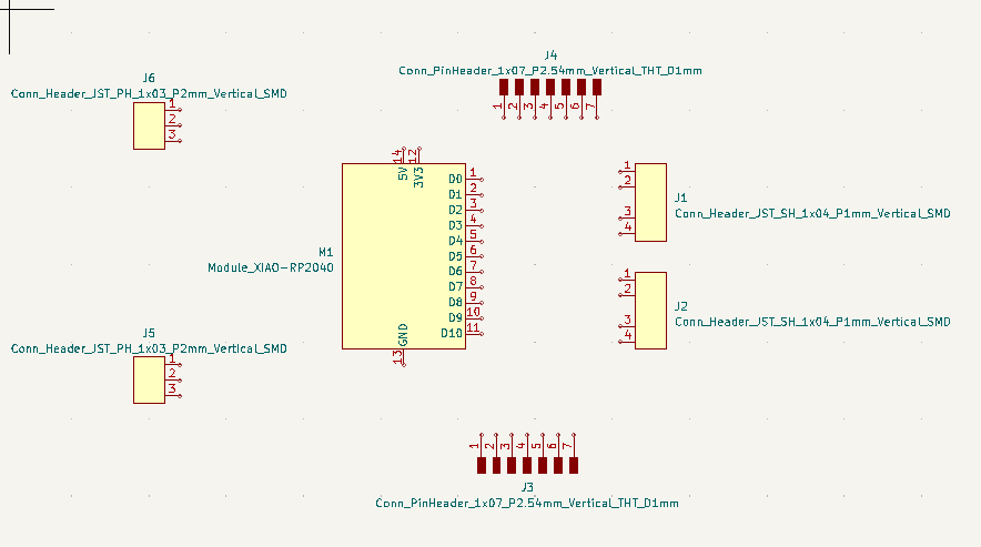
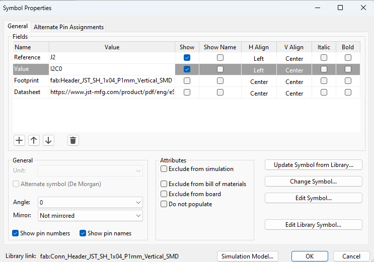
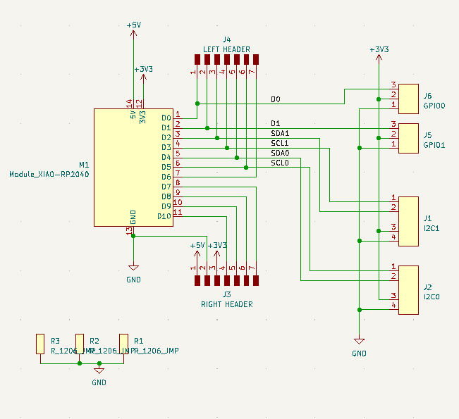
PCB Editor
Now it's time to lay out the components on my future circuit board. Open the PCB Editor from the project window, or hit the Switch to PCB" icon.
- Use the
 update board from schematic tool to bring your schematic parts into the new PCB design. The parts will come in as a group.
 - Lay out the components in a way that makes physical sense, using the same movement commands and keystrokes as in the schematic editor. Now, orientation and position are crucial! Traces can't cross over each other, so you need to minimize or eliminate crossing points. Traces can go under components though, which is the key to success.
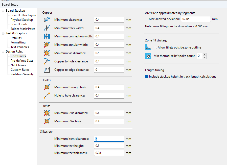
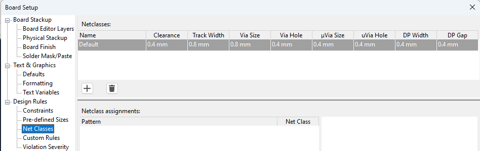
- Set up "design rules". We're going to be milling this board with a 1/64" (0.4 mm) wide bit, so it's crucial that all traces and pads are separated by at least 0.4 mm. Many of the other rules (like for silkscreens) don't matter.
- Set up standard trace widths. In the File / Board Setup menu, choose "Net Classes". I changed the width of the default tracks to be 0.8 mm, with 0.4 mm spacing between them. This will hopefully give nice big phat traces that are easy to mill and can carry lots of power if needed.
- I also created a thinner track width in the "Track" dropdown, of 0.4 mm, to connect to small components and pads.
- The thin blue lines are "airwires", and show which pads need to connect to which. Replace these with actual traces using the
 Route Tracks tool. As I drew, I made sure to keep everything as widely separated as possible while keeping the overall design as compact as possible.
 - Use the Design Rules Checker in the "Inspect" menu to find any problems with your board and make sure it's manufacturable. In my case, this found a whole bunch of tiny little traces that I couldn't see buried under the intended ones.
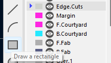
- To make an outline for your board, activate the
Edge.cutslayer on the right side of the PCB editor, and draw a rectangle of the desired size.
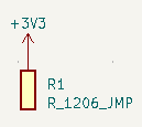
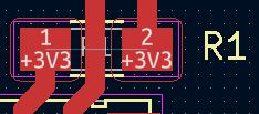
Crossing the Streams: The Jump Resistor Trick
Often, two traces have to get past each other, and there's no way to route them around to avoid crossing on a single-layer board. That's why most professional circuit boards have two or more layers. To make it work, the secret is to add zero-ohm SMD "Jump resistors" to your design, so traces can "hop over" each other. These are included in the Fab KiCAD library asR_1206_JMP. In the schematic editor, they have only one terminal, so you can stick them anywhere. In the board editor, they have two pads carrying the same signal, so you can use them to hop over other traces. The only drawback to this method is that it leaves "air wires" between the two pads of the jump resistor, which causes error in the design checking phase, I'm not sure if that can be avoided.
In the end I needed three. I feel like I could have made it less if I were smarter at solving the routing puzzle.
Finished First-Draft Board
Here's what my final first-draft board design looked like: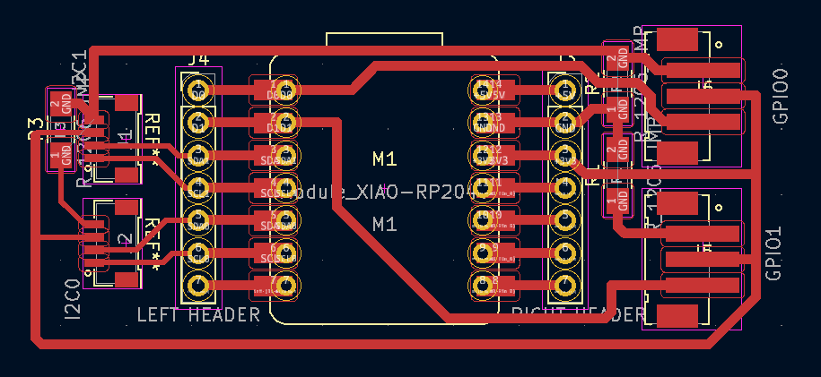
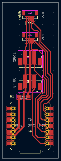
Second Draft: "Slim"

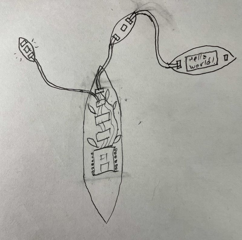
Next steps: The "Beansprout" Aesthetic
And that's when the "Beansprout" concept really started to take off, because now it starts to look like a beanstalk, or something plant-like, with rising tendrils for the traces.But it's also when I ran out of time. When I actually build this, I'm going to re-do the traces so they have smooth organic curves instead of angles, add some cosmetic "leaves" to the design of the copper. And the daughter boards that plug into the design will be leaf or seed-pod shaped. I made a pencil sketch of what the overall idea would look like, and exported the traces to Illustrator as an SVG and made an initial stab at redrawing the traces as smoothly curved lines and adding leaves. Unfortunately I didn't have time to perfect this and I'm a terrible artist, but you get the idea of what I'm going for. I tend to think in straight lines, and this sort of organic drawing isn't in my skill set. I'll revisit this soon!