- Assignments
- Fab Inventory
- KiCad
- Atari Punk Console
- Errors
- Group assignment
- Files
- Thursday lecture notes
- Lecture notes
- Designing circuits
Electronics Design
This week is about designing electronics and getting familiar with KiCad. For this week I want to learn more about working with sound in combination with the XIAO ESP32. One idea is to make a small board with which I can record audio and play it back using a microphone and a speaker, or just with a speaker to play audio or tones. I also want to add headers to the pins that I’m not using so I can use it as a devboard as well. For this I’m using Adrians FabXiao as a reference.
Maybe this week I can make:
- a board that takes pitch & volume detected with a microphone and outputs a square wave that changes frequency and amplitude based on that pitch & volume. This could be integrated into a mask where the microphone is placed in front of your mouth.
- an Atari Punk Console or Baby 8 sequencer
- A board to attach e-textiles variable resistors to, with a potentiometer in between as the known resistance; what I do now is just replace the resistor manually in a breadboard when I’m testing e-textiles swatches
Assignments
| Progress | Task |
|---|---|
| Done | Group assignment: use the test equipment in your lab to observe the operation of a microcontroller circuit board (as a minimum, you should demonstrate the use of a multimeter and oscilloscope) & document |
| Done | Individual assignment: design a development board to interact and communicate with an embedded microcontroller |
| Done | Documented what you have learned in electronics design |
| Done | Explained problems and how you fixed them |
| Done | Included original design files (Eagle, KiCad, etc.) |
| Done | Included a ‘hero shot’ |
Fab Inventory
The Fab inventory is a list of all of the recommended components and tools that labs in the Fabacademy network should have. It also lists many of the electronics components that we have in our lab, so I’m using it as a starting point. All components in there are also in the KiCad fab library. Below some components of interest:
| Digital microphone | MIC MEMS DIGITAL I2S OMNI -26DB |
| Analog microphone | MIC MEMS ANALOG OMNI -42DB |
| Speaker | SPEAKER 8OHM 250MW TOP PORT 81DB |
| Micro SD card reader | CONN MICRO SD CARD PUSH-PULL R/A |
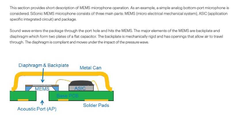
I was looking through the datasheets of the parts above, and they all required various extra components that made the circuits a little too complicated for a first electronics design week. Many of the things I want to try are part of future weeks such as input devices. What I can do is make a development board with some extra features built in like an analog microphone and a small speaker and leave the digital microphone and SD card reader out for now.
I decided on the analog microphone because it seemed a little less complicated. The analog one has the circuit below in the datasheet as the interface circuit. In the datasheet you are refered to the design guide. There I learned more about how this tiny microphone works.

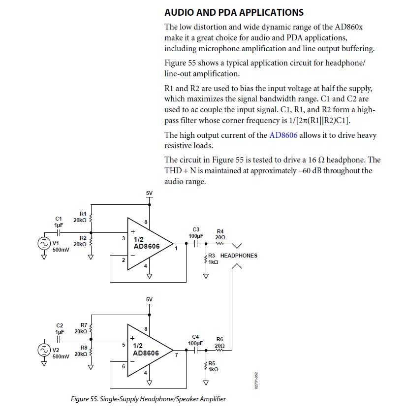
I looked up what this external gain is: it’s the amplification of the input voltage and is needed because the sound vibrations that a microphone picks up are very weak. Setting microphone gain is important in having a good audio output. For this I have to use an Opamp. I looked for one in the fab inventory and this is the one I found, so I guess I’m integrating it into the circuit. In the datasheet for that one there is this example circuit fo use with headphones:
At this point, I was a little bit lost againand I’m making it a little bit complicated again. So my new plan is to make a FabXiao board with just a speaker integrated, and maybe an LDR instead of a microphone because they are way simpler. That way I can still use a variable input to play with sound. I’ll have another look at microphones again soon.
KiCad
I’m currently on KiCad 6 but I saw that KiCad 7 is out and read that KiCad 7 is a significant upgrade from KiCad 6, and comes with a number of exciting new features as well as improvements to existing features so I wanted to upgrade for this week. I only have about 5GB of free space on my hard drive, so I’m first removing KiCad 6 and all of its components and then starting afresh. I then downloaded the Fab Electronics Library for KiCad here and followed the steps as described in the readme.
I’ve made board before and documented the steps here.
BOM
I’m going to start by adding all of the components that Adrian used for his FabXiao, and work from there.
These are the parts on Adrians board:
| 1x | XIAO ESP32C3 | |
| 1x | 0 Ohm resistor | As bridge |
| 1x | 499 Ohm resistor | For switch |
| 1x | 1 kOhm resistor | For LED |
| 1x | LED | |
| 1x | Button | |
| 3x | Female 1 row horizontal header | |
| 1x | Male 2 row vertical header |
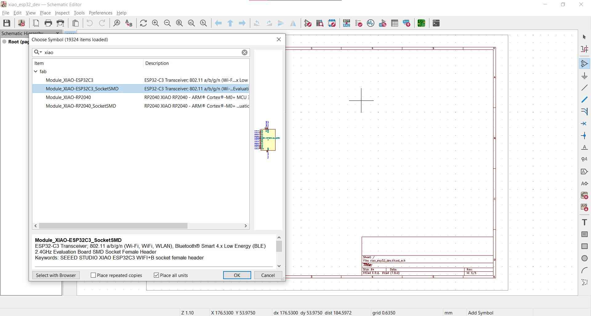
I’m going to take all of these from the fab library in KiCad.
What I want to add:
| 1x | SPEAKER 8OHM 250MW TOP PORT 81DB |
| 1x | Add 100 Ohm resistor between speaker and ground pin (see http://arduinolearning.com/learning/basics/arduino-speaker-example.php) |
| 1x | SENSOR PHOTO 940NM TOP VIEW 1206 |
| 1x | Add 10K resistor between collector and 5V (see http://fab.cba.mit.edu/classes/863.18/CBA/people/alex/week-10-output-devices/index.html) |
For another day:
| 1x | MIC MEMS ANALOG OMNI -42DB |
| 1x | Needs an IC OPAMP GP 1 CIRCUIT SOT23-5 |
| … | And some other resistors |
EEschema
| Shortcut | Navigation |
|---|---|
| A | place symbol |
| M | move component |
| G | grab and move a component (without breaking connections) |
| W | place wire (shift + w) |
| P | place power symbol |
| Ctrl + L | place global label |
| R | rotate |
| C | copy |
| E | change the value of components |
| D | open datasheet |
| Scrolling | zoom |
| Scroll button and drag | pan |
| Space bar | resets dx dy value, useful for measuring distance in the PCB editor |
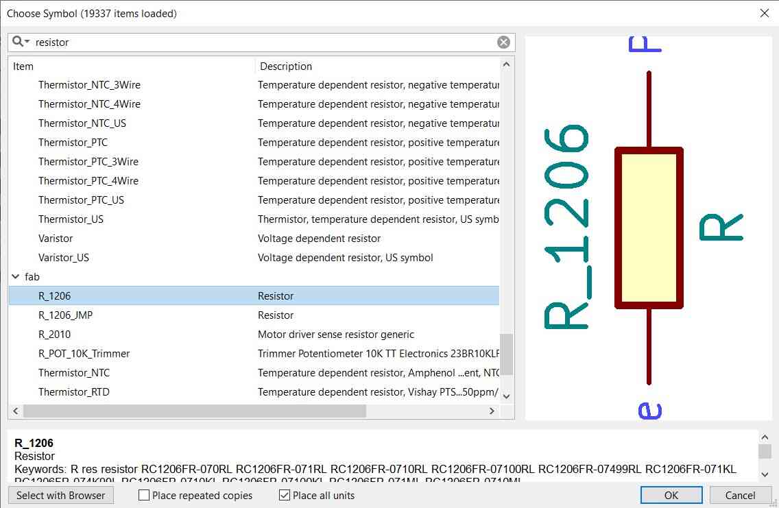
I started by placing all of the components on the Eeschema sheet. By pressing A you can add a symbol, after that you can keep clicking and adding more symbols.
Here are the current parts placed:
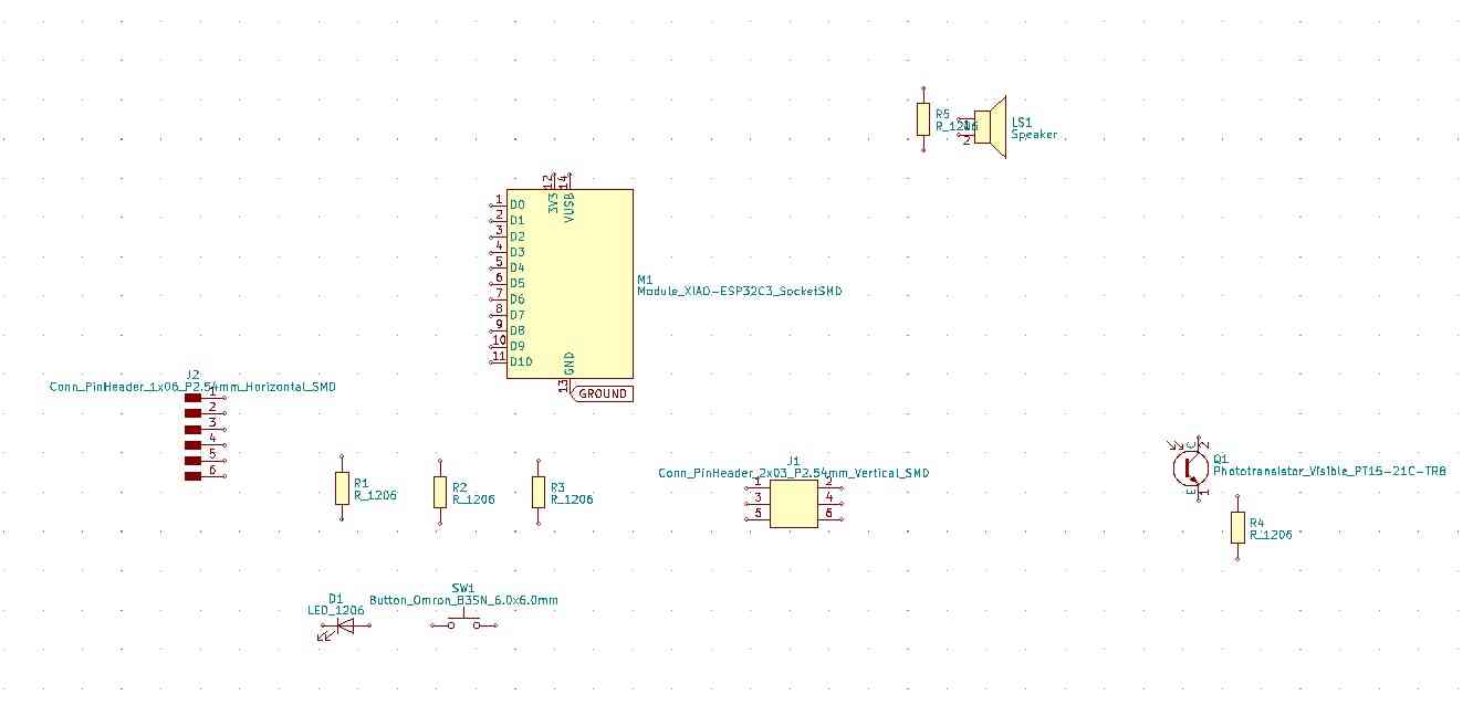
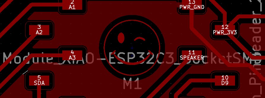
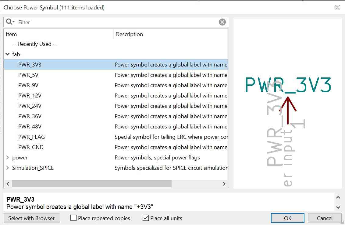
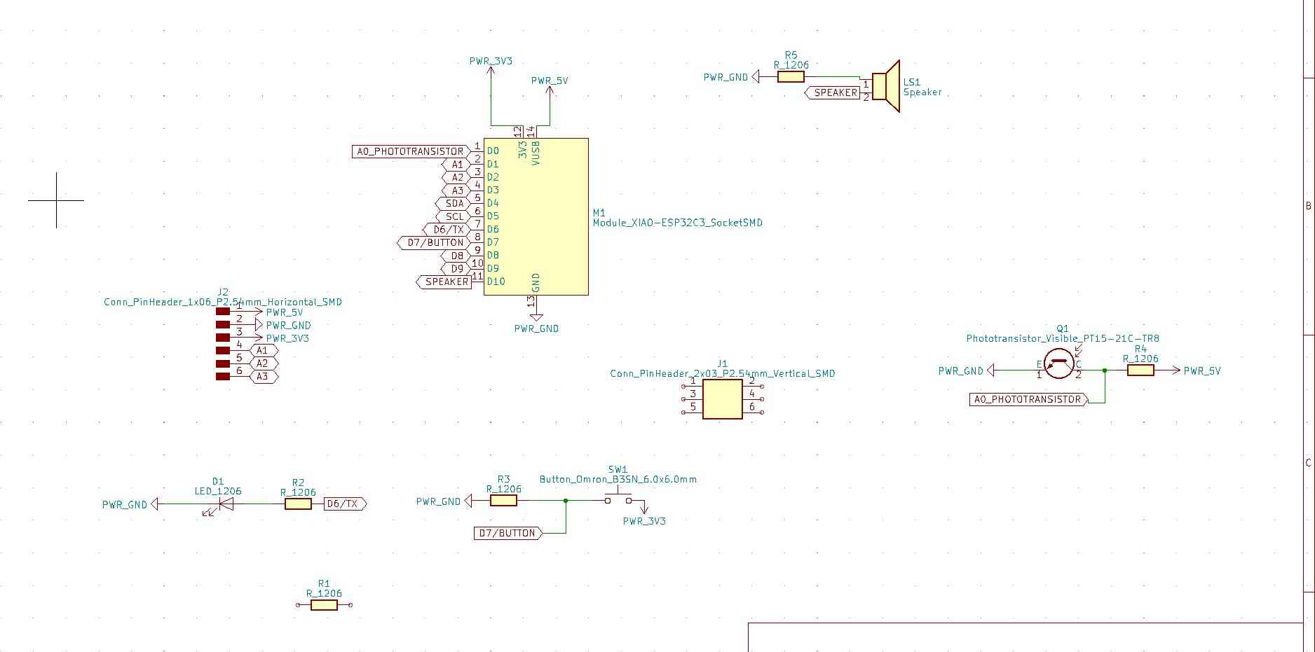
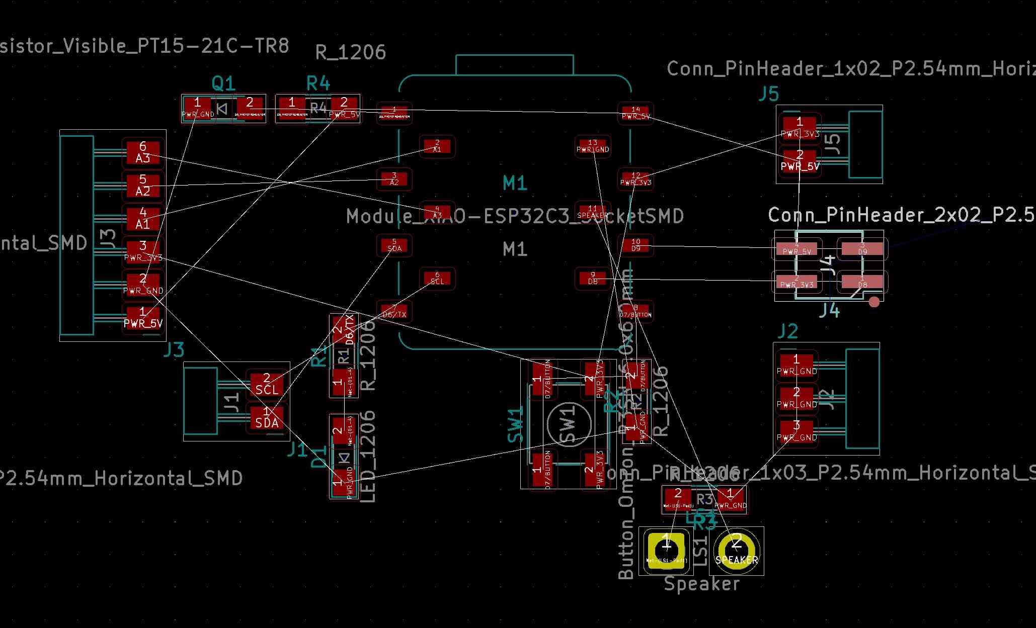
Then I connected them with global labels; power and ground were added with power symbols. I used Adrians board as a starting point but changed some things because I added the phototransistor and speaker. Only later I saw that Adrian had also made a phototransistor module for the board; in any case I’m integrating it.
I saw in the datasheet of the ESP32 that “All digital IO pins are bi-directional, non-inverting and tristate, including input and output buffers with tristate control” so I’m giving them the tristate label if I’m not specifically using them for something else.
Most labels attached:
- All of the pin headers in the fab library that are called male headers are also used for pin sockets as far as I can tell
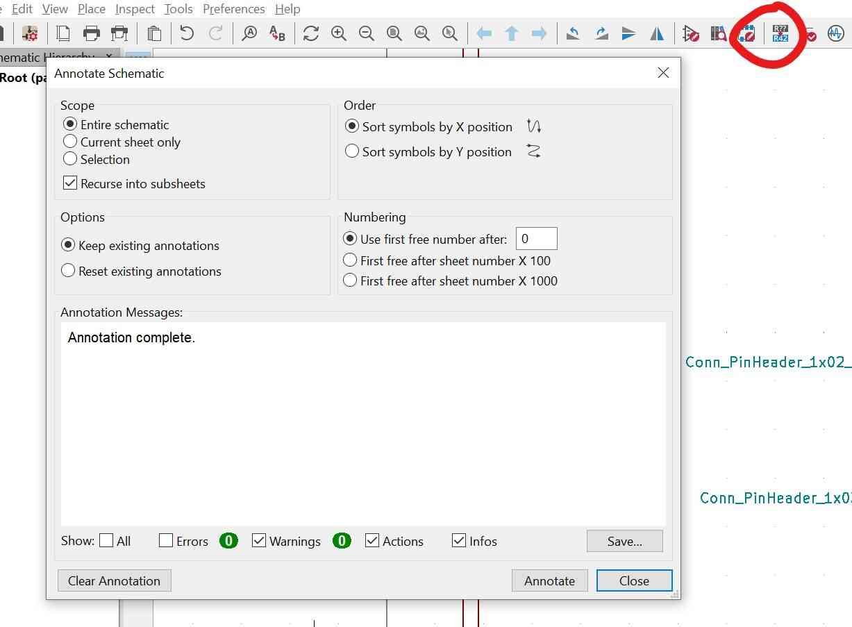
Annotate schematic
After connecting all of the pins, I’m annotating the schematic symbols by clicking on the button circled in red. I didn’t run into any errors there.
Electrical Rules Check
Then I did an electrical rules check where I got these errors:
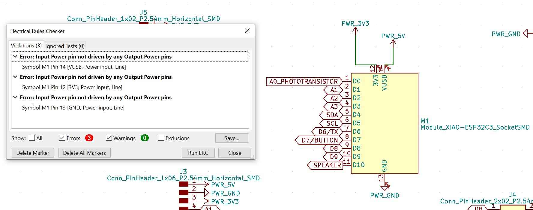
A quick search revealed that I needed to add special power flags to tell KiCad where the power is coming from; KiCad has no idea otherwise.
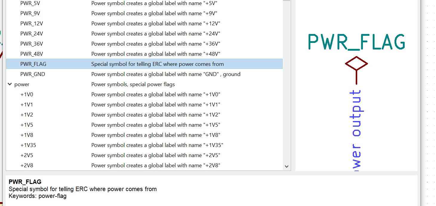
Now I’m not getting any errors:

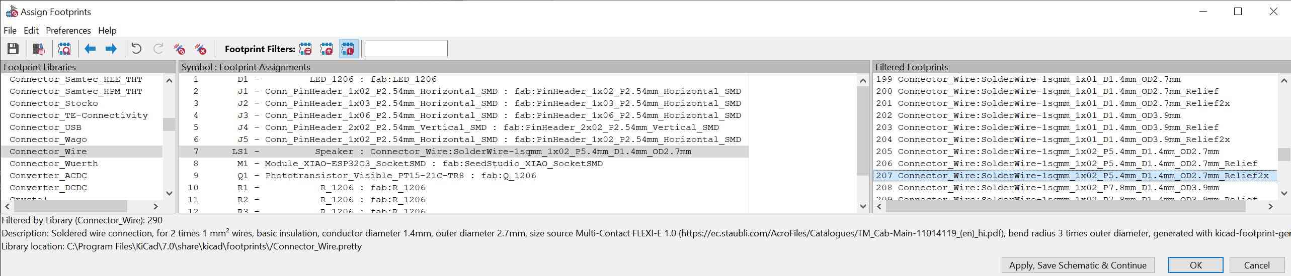
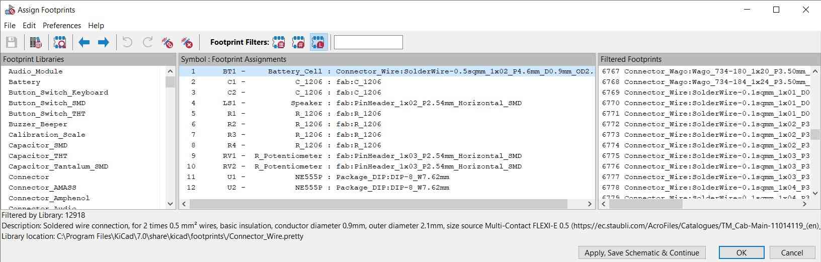
Assign footprints
Assigning the footprints; if everything is okay press apply, save schematic & continue. You can see here for example that the footprint for the speaker is just a pinheader.
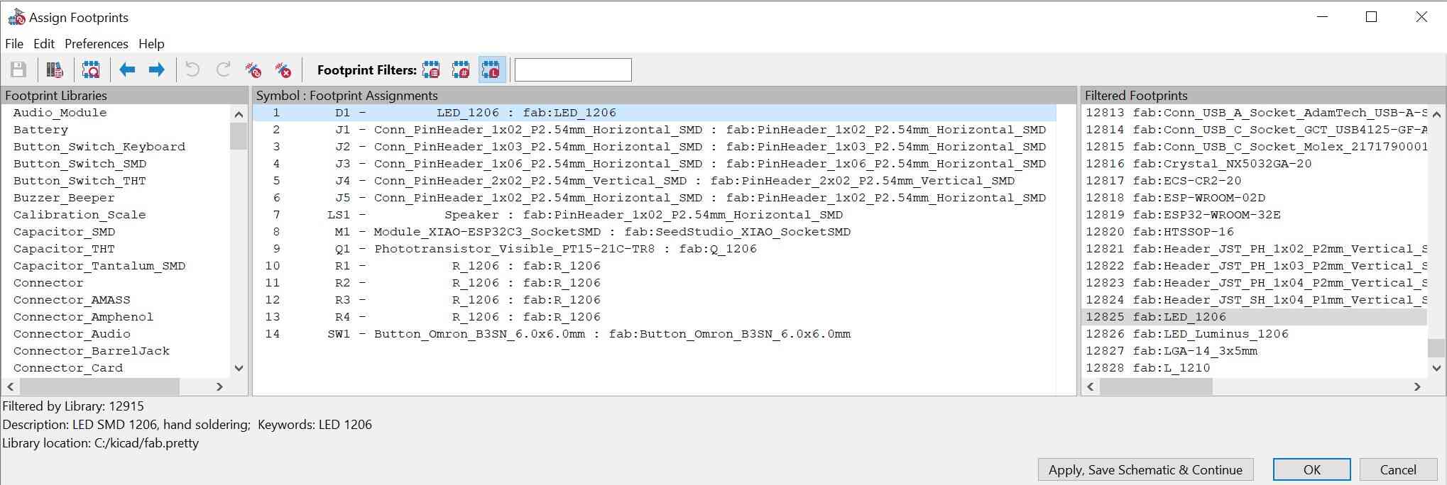
What I’m going to do is add alligator clips instead so I can also use this board to test e-textiles speakers. I deleted the associated footprint and added two through hole solder pads.
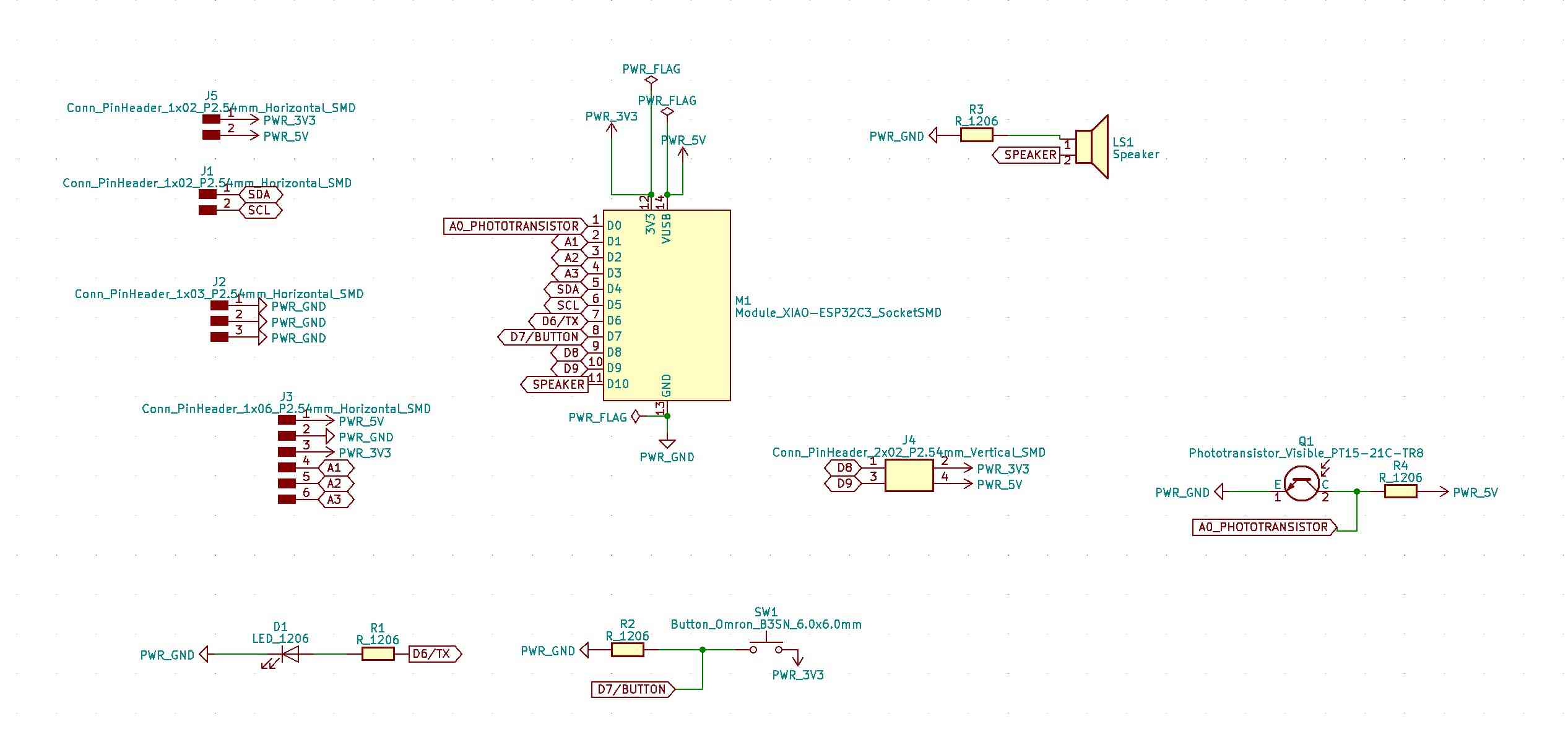
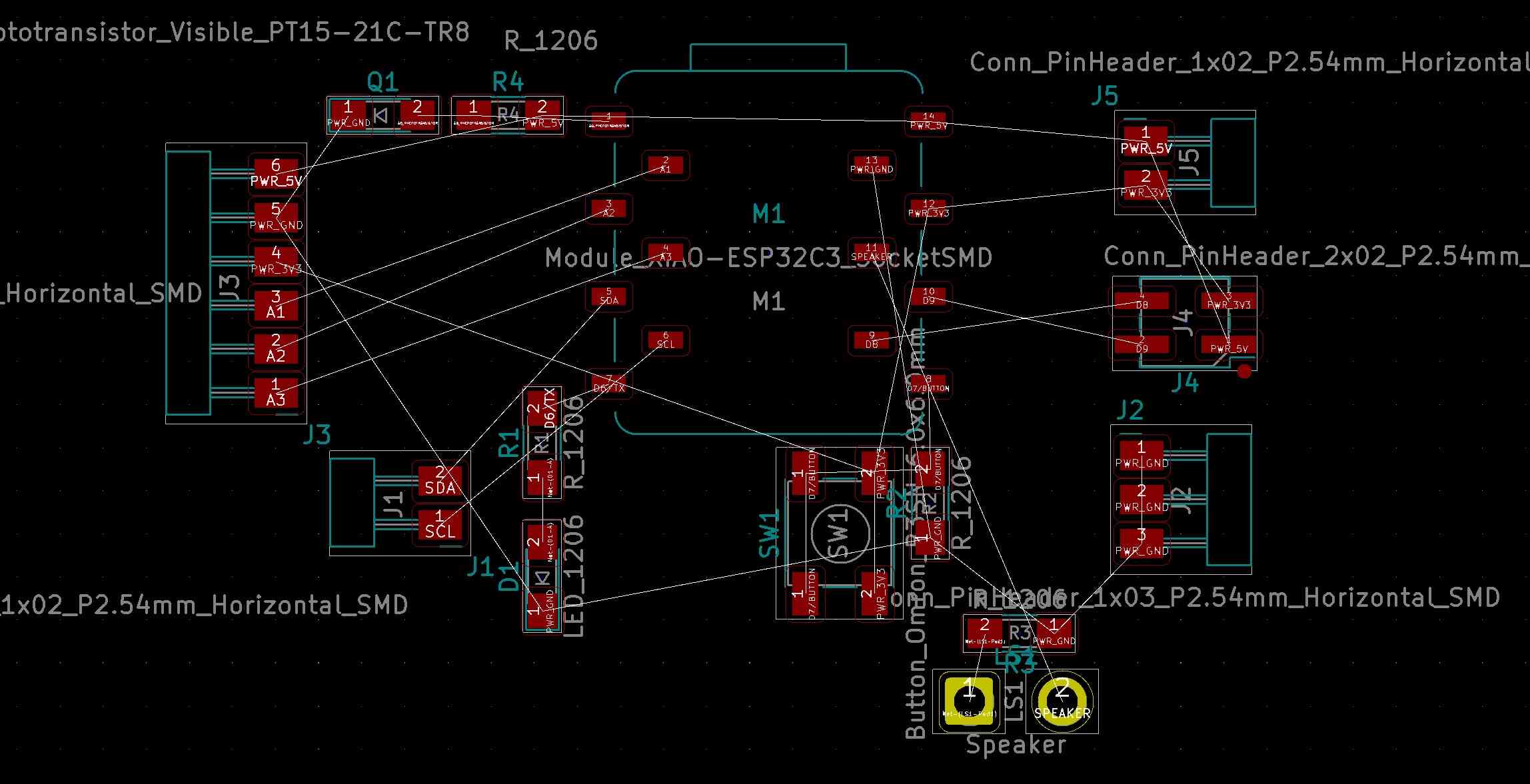
Generating a netlist is no longer necessary, so now I’m ready to go to the PCB editor. This is what my schematic looks like now:
PCB editor
Board Setup
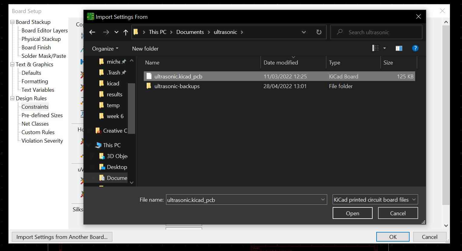
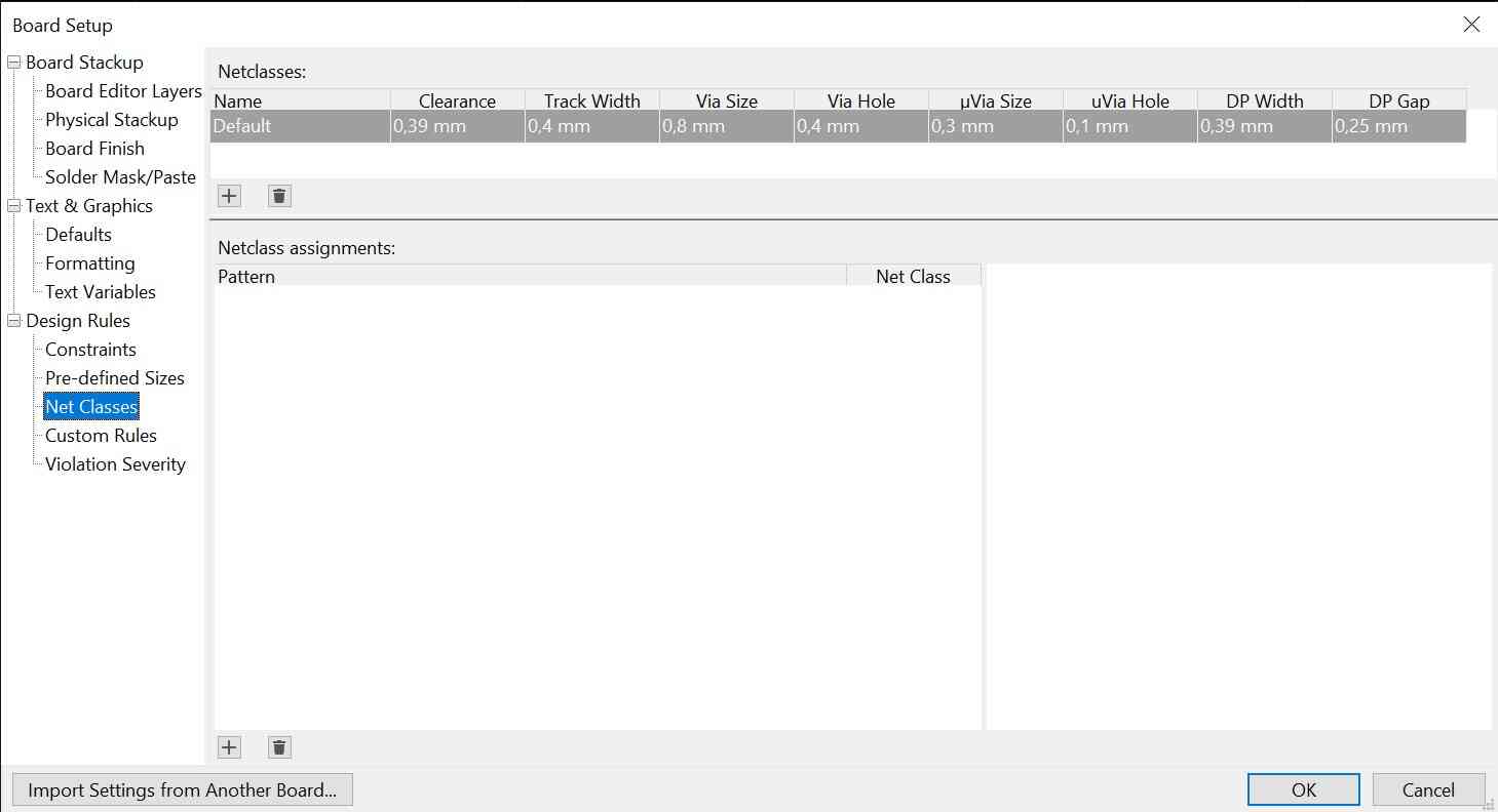
Now in the PCB editor I first had to specify the board setup (File > Board Setup). I wanted to copy it from my documentation but then I saw this option to import settings from another board, so that’s what I did instead. I made a board with an ATTiny, ultrasonic sensor and neopixels last year.
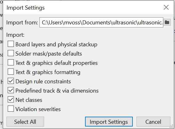
I saw that some names were slightly different (KiCad 5 vs 6 vs 7) but I think it should be good otherwise. Here you can see the automatically updated settings in the design rules constraints & net classes.

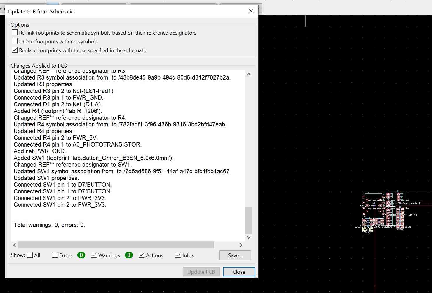
Update PCB from Schematic
| U + delete | delete entire track |
| B | fill/update copper pour |
I updated the PCB and the rat’s nest appeared. I thought that the way the pads are placed for the socket for the XIAO board looked weird so I looked up other sockets in the fab library, but all of the vertical ones are like that so I think it should be ok.
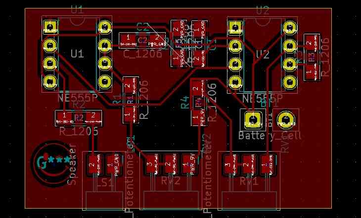
I moved the parts a little bit apart so I could start routing. At this point I realized that I hadn’t given values to the resistors, but I don’t think it matters too much (later I added them to the schematic).
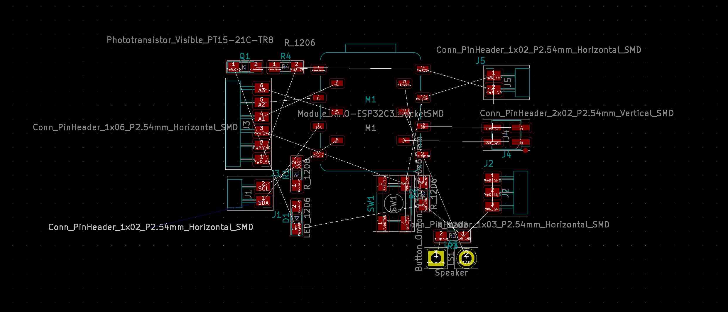
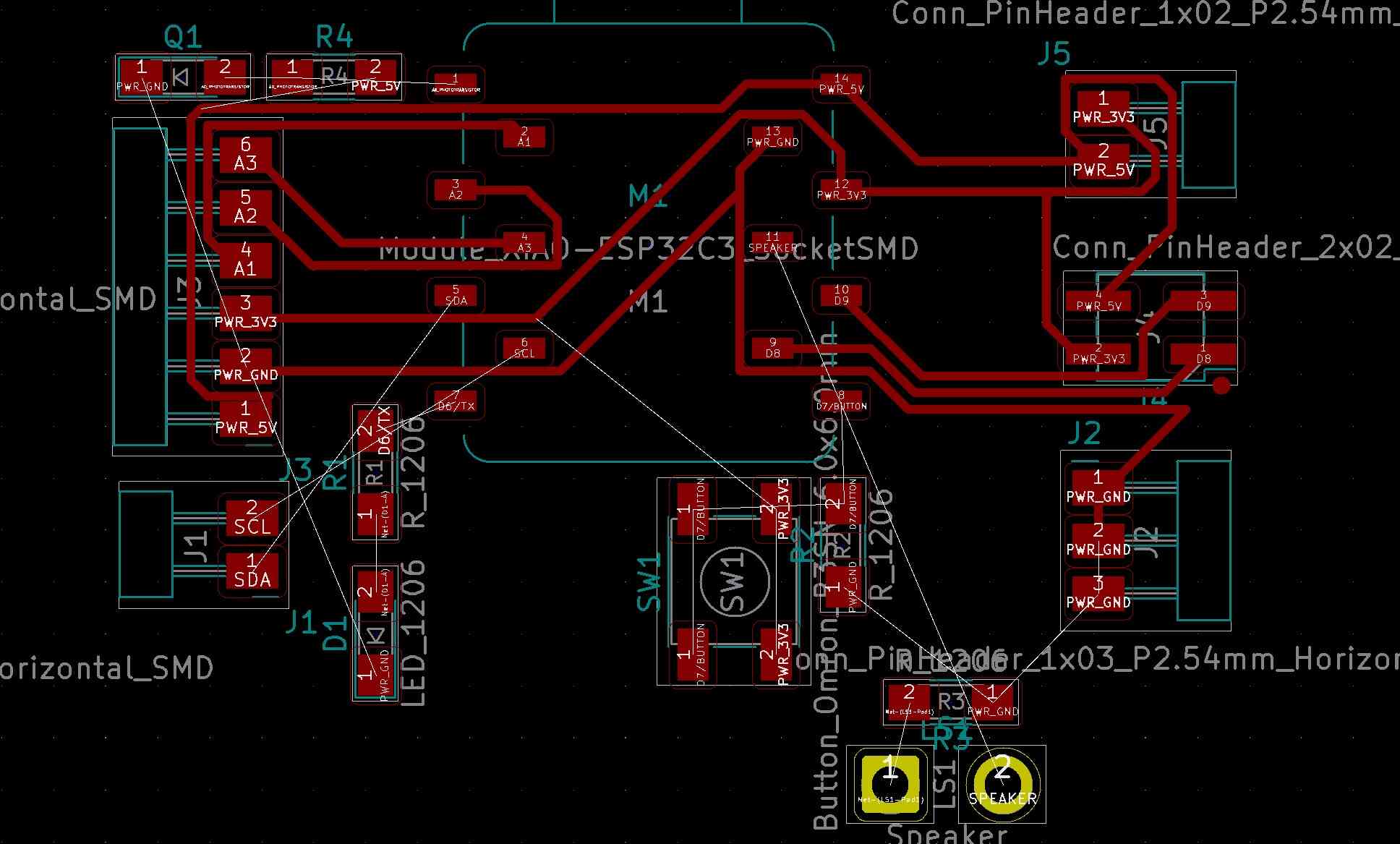
I pressed X and started routing; I noticed quickly that some of my sockets would be better off if they were mirrored. I tried to use the same orientation as Adrian but I think as he was working in Eagle that didn’t work out. I went back to Eeschema and mirrored the sockets horizontally, and went back to the PCB editor. I deleted all of my traces so far with Edit > global deletions. This is before updating:
And this is after; a couple of links that aren’t crossing anymore which is nice.
Stuck again:

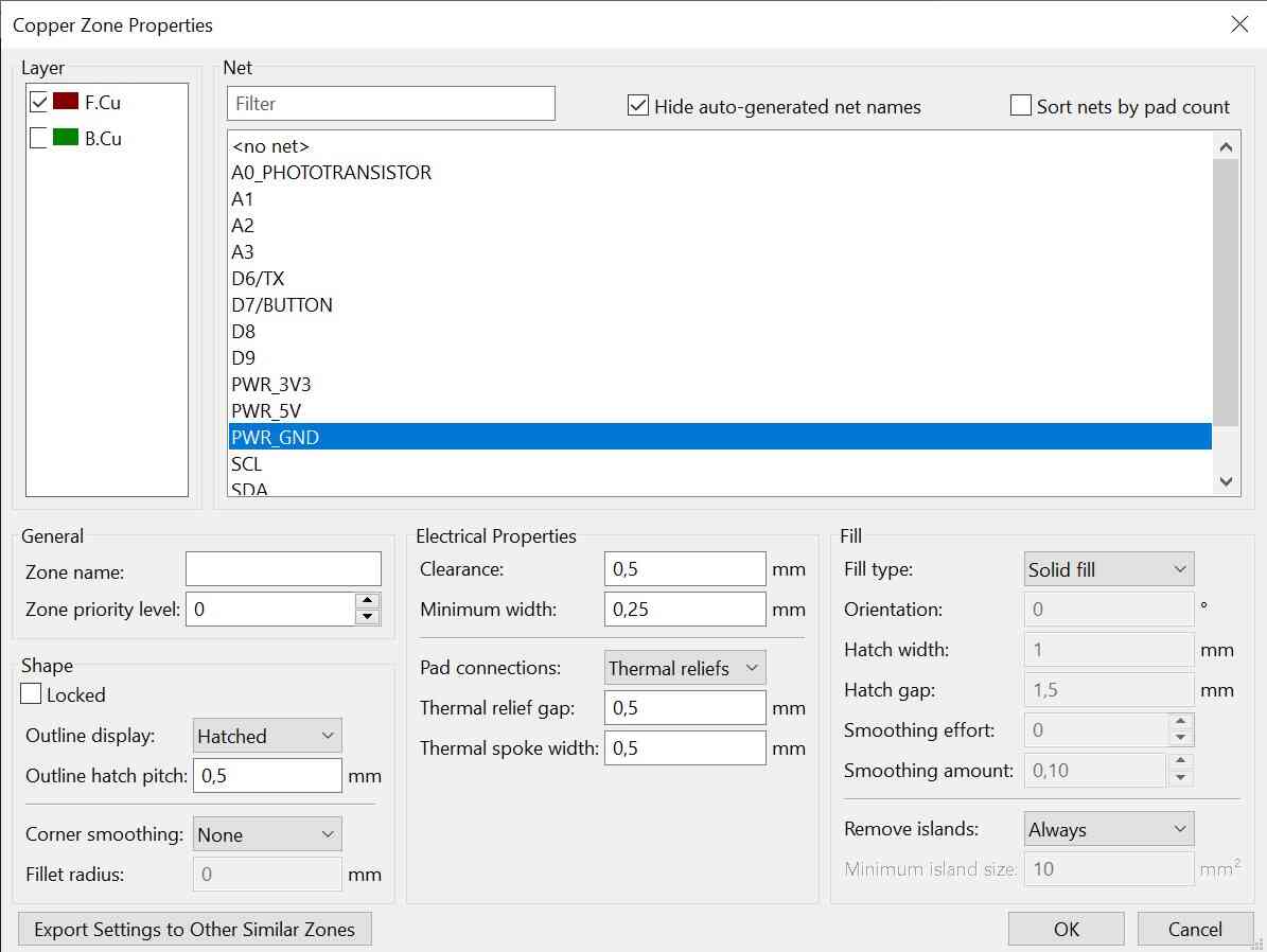
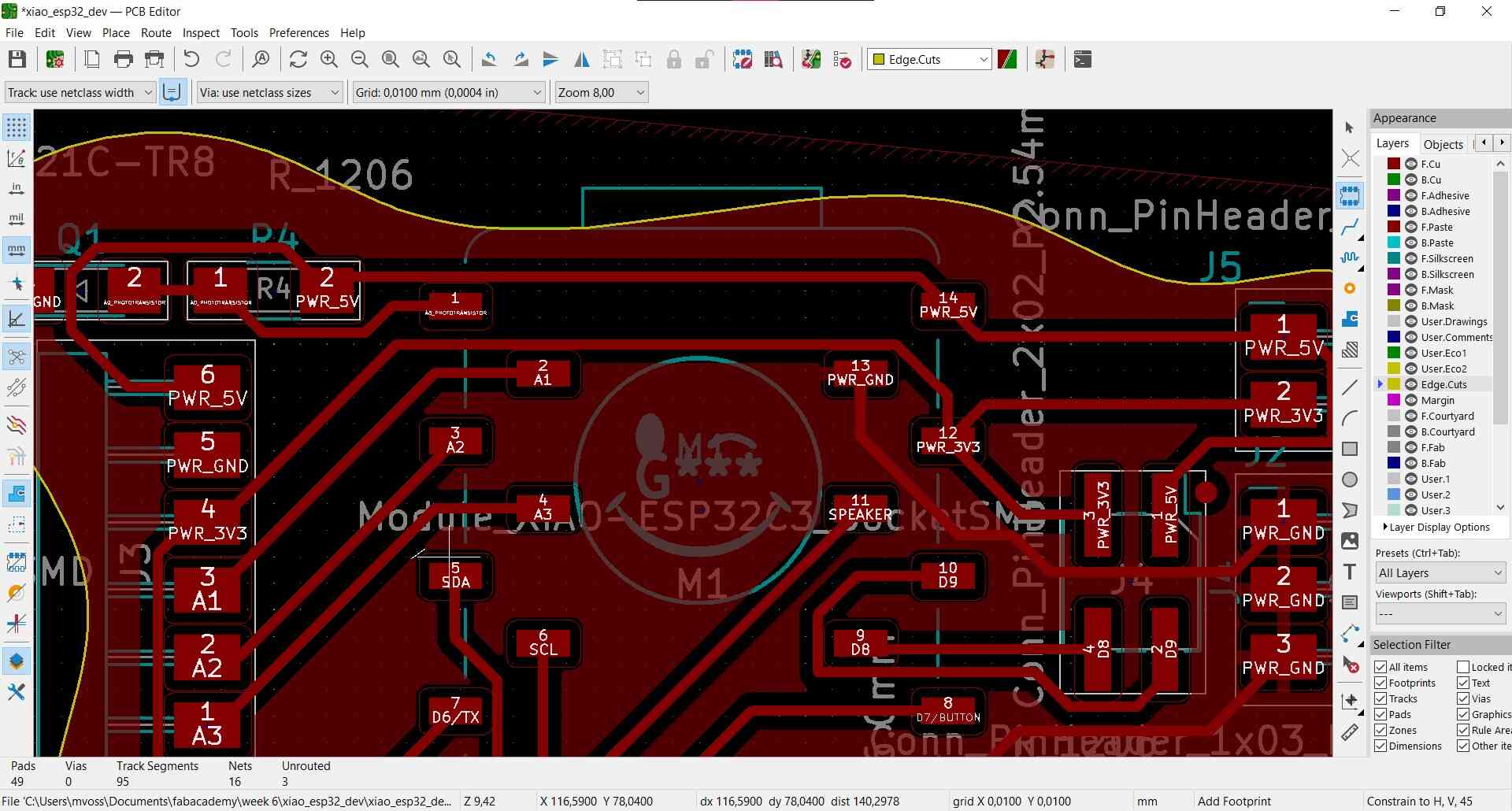
Then finally I was almost there; with a copper pour for ground (layer F.Cu > Ctrl + Shift + Z) the board was fully connected (Edit > Fill all zones, or B).

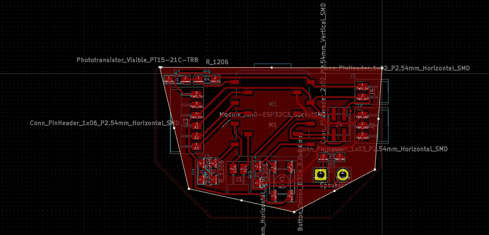
Slightly more fun, the shard board:
This is the board in 3D view:

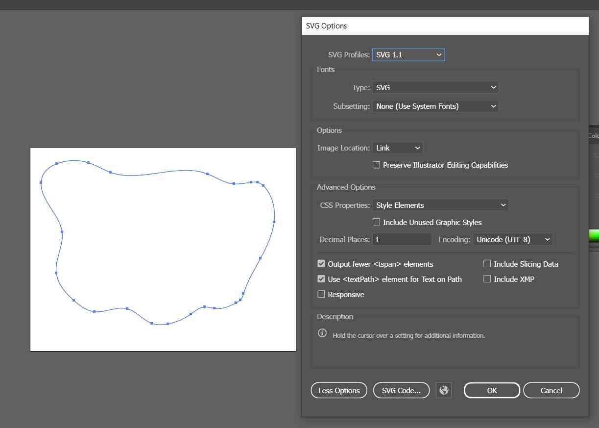
I also wanted to try to make a custom edge cut; for this I used Illustrator. I pasted a screenshot into illustrator and made a blob shape. Then I saved it as an svg.
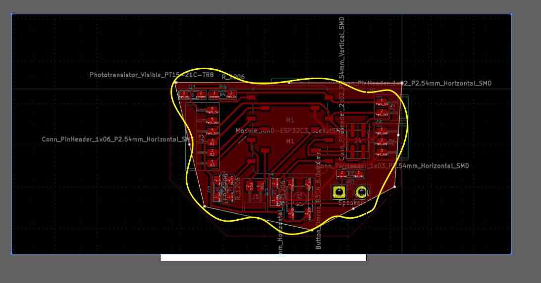
Then I imported it as an edge cut:
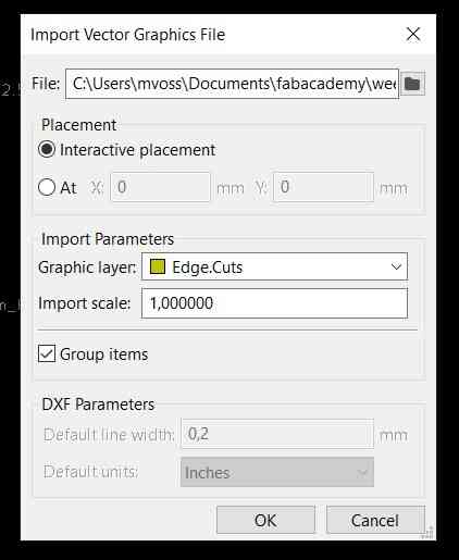
Importing it was easy, but it’s very big and I couldn’t find a way to scale it. I measured the distance in KiCad and scaled the svg in Illustrator, then imported again; however the scale in Illustrator and in KiCad didn’t match up. 60mm in Illustrator turned into about 45mm in KiCad. I decided to then scale it by 25% while importing and then it was fine. I did the copper pour again.
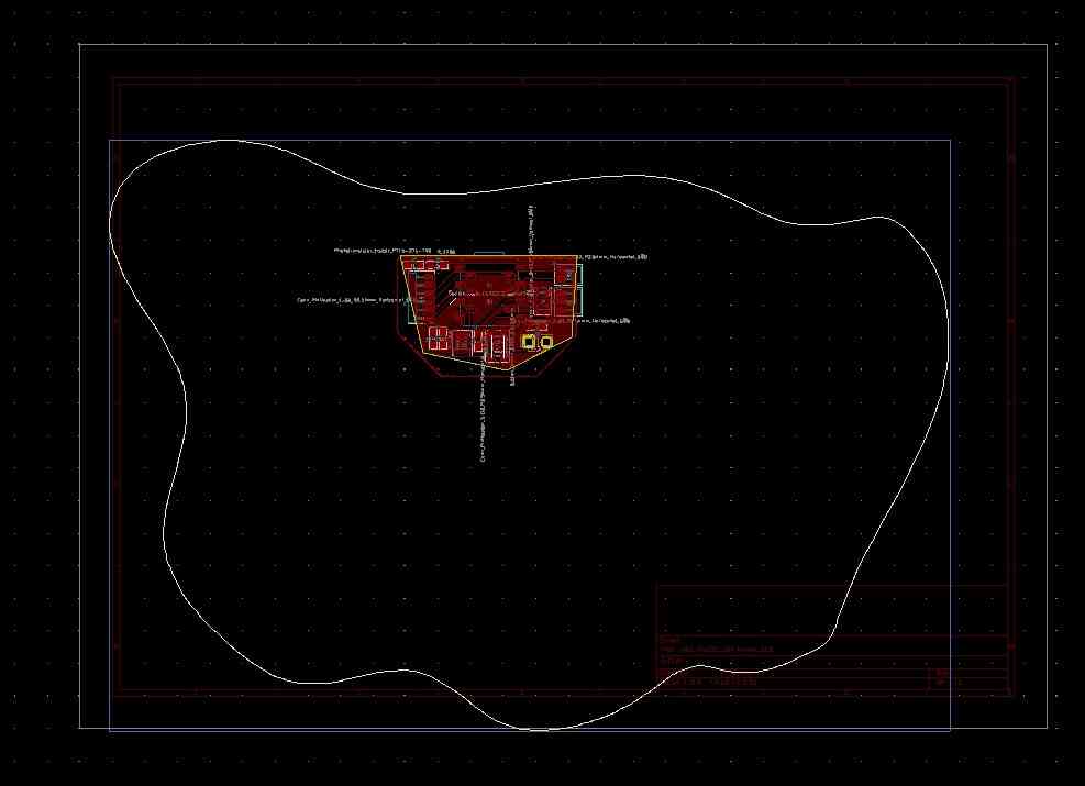

Image Converter
Then I wanted to try out the image converter. You can use Image Converter to convert images to a file format that KiCad understands, which is useful for putting logos or other images on a PCB. You can import a bitmap image and convert it to a footprint, symbol, postscript or drawing sheet. I exported to a footprint and symbol and placed them in a new custom library called vossen. I then added this library the same way I added the fab library.

Only now it’s just a logo and not actually in the PCB, so I have to change the layers of the smiley.
Footprint Editor
I first tried to edit it in the PCB itself but then I would have to change it every time, so I opened it in the footprint editor instead. If you press E (edit) while hovering over one of the lines you can change the layer. You can only do this for one shape at once. For the 10mm smiley I left the circle outline on the silkscreen layer.
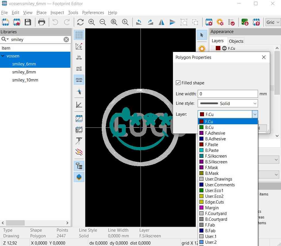
Now every time you take off the board, you get a wink.
Atari Punk Console
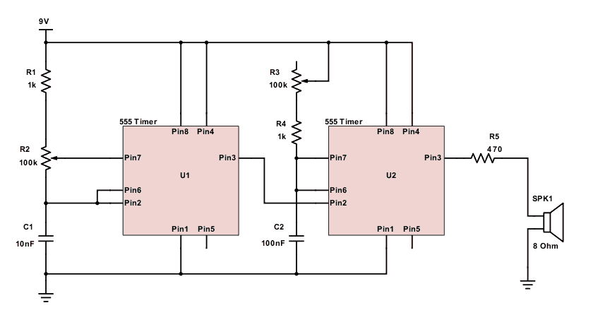
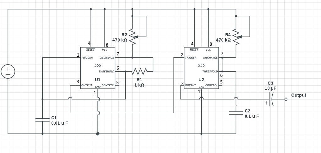
Next I wanted to make an atari punk console (APC) using two 555 timer IC’s; we have a lot of the NE555P chips. An APC is a simple DIY noisemaker circuit, and I think it would be a good first audio project. This is the schematic found on here; that’s also where I got the BOM from.
So what is an Atari Punk Console:
Atari Punk console is an astable square wave oscillator driving a monostable oscillator that creates a single (square) pulse. There are two controls, one for the frequency of the oscillator and one to control the volume. The controls are usually potentiometers but the circuit can also be controlled by light, temperature, pressure etc. by replacing a potentiometer with a suitable sensor (e.g., photo resistor for light sensitivity). Most of the time there is also a power switch (often a toggle switch) and a volume knob.
BOM
| Amount | Component | Notes & changes |
| 1x | Speaker (minimum 0.3W) | Connect with through holes; I’m going to use a 0.5W 8 Ohm speaker |
| 2x | 555 timer chips | |
| 1x | C1: 10 nF capacitor | |
| 1x | C2: 100 nF capacitor | |
| 2x | R1, R4: 1 kΩ resistors | Can also be slightly higher or lower; it’s in series with the potentiometer to make sure it doesn’t reac |
| 2x | R2, R3: 100k potentiometers | can also have a higher limit |
| 1x | R5: Resistor, 470 Ω | I might change this into a 10uF capacitor as per the instructables schematic, which uses the capacitor to filter out noise. Whether the resistor is necessary depends on the rating of the speaker used (check comments here) |
| 1x | 9V battery connector | Connect with through holes |
| 1x | 9V battery | Connect to 9V connector |
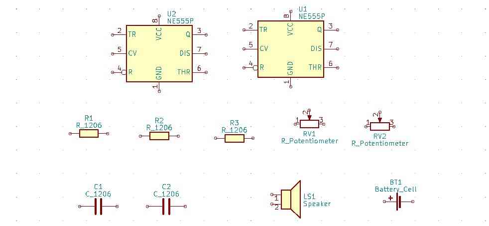
I looked for the IC in the footprint library and found this one. I measured the chips we have and it should fit.

For the battery connector, I just added a battery symbol and I’m going to assign a footprint to it with two through holes. The potentiometer I want to replace with e-textiles sensors later and I don’t want to add it on the board directly, so I’m going to give those female header pins so I can easily swap sensors. I could then also replace the potentiometer with an LDR for example.
I connected them as in the schematic; I also found the schematic on wikipedia that was slightly different but I decided to stick with the one from above (the other one can be found here). I noticed that the potentiometers were connected in two different ways, one as a voltage divider using both pins and one as a rheostat (variable resistor) using only two pins connecting to the data pin and VCC. In the picture on the website however there are only two pins connected on both potentiometers so I think the potentiometer on the left doesn’t have to be connected to ground.
I didn’t really trust the schematic I was following so I also made a version based on the instructables schematic; I didn’t add a polarized capacitor for the speaker though, I kept the resistor. I can still swap the resistor out for the capacitor after milling the board because the footprints are almost the same.
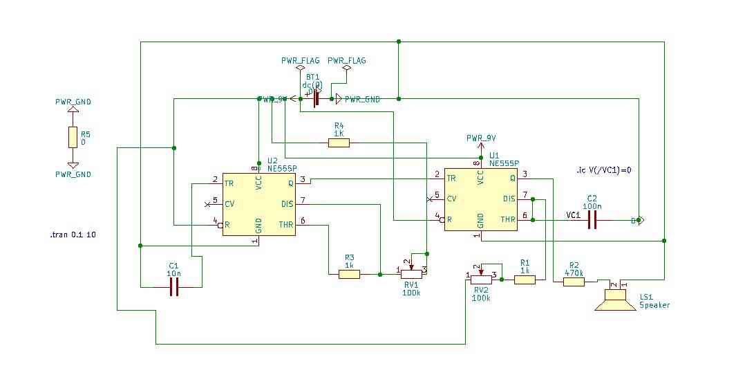
This is the new schematic I’m keeping as a reference:

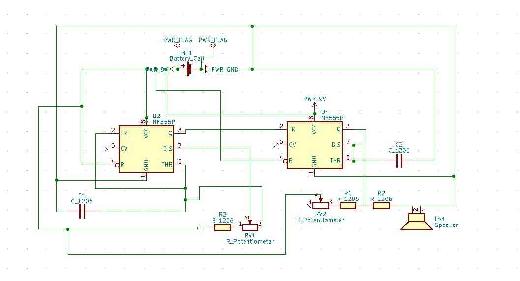
This is the second iteration of the schematic that I’m continuing to work with:

ERC produced 0 issues. Footprints:
Rat’s nest:

I managed to connect everything except for the two ground areas. I tried a couple more times but it didn’t work so I added a 0 Ohm resistor to make a bridge. The line is still there to connect the two areas so I think I didn’t label them correctly, but that doesn’t matter for milling the board.
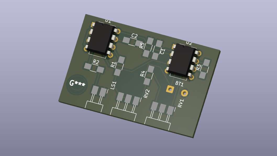
Here the raytraced 3d render of the board:
SPICE simulation
I’ve never tried simulation, and I saw that there was an integrated simulation called SPICE in KiCad, so I wanted to try it out. I found this short video for KiCad 5; some steps are slightly different.
There are a couple of standard functions you can call:
- AC Sweep
- DC Transfer
- Operating Point
- Transient
Steps
- A > look for Spice > add 0V reference point > place where you want to measure
- Make sure all components have values and written in a way that SPICE understands
- Add text with function and values; when checking how a capacitor charges set an initial condition of 0 (otherwise SPICE assumes the capacitor is fully charged)
My schematic looks like this with values and functions:
I tried to do the same as in the video but I just got errors:
Note: Compatibility modes selected: ps a
Error: Missing token in line 6:
rv1 __rv1
Please correct the input file
Error: Missing token in line 7:
rv2 __rv2
Please correct the input file
Warning: Cannot read 2 nodes in line __rv1
Instance not ready for .probe command
Warning: Cannot read 2 nodes in line __rv2
Instance not ready for .probe command
Warning: Cannot read node 2 in line __u1
Instance not ready for .probe command
Warning: Cannot read node 3 in line __u1
Instance not ready for .probe command
Warning: Cannot read 2 nodes in line __bt1
Instance not ready for .probe command
Warning: Cannot read node 2 in line __u2
Instance not ready for .probe command
Warning: Cannot read node 3 in line __u2
Instance not ready for .probe command
warning, can't find model 'speaker' from line
ls1 0 probe_int_net-_ls1-pad2__ls1 speaker
ERROR: mal formed B line: bt1 __bt1
Error: ngspice.dll cannot recover and awaits to be detached
Note: can't find the initialization file spinit.
******
** ngspice-39 shared library
** Creation Date: Feb  9 2023   06:17:51
******
Note: No compatibility mode selected!
Circuit: *
Warning: No job (tran, ac, op etc.) defined:
run simulation not started
So far not so good.
Errors
File corruption after computer shutdown
After my computer shut down I ran into the following error when trying to open an autosave file of the PCB:
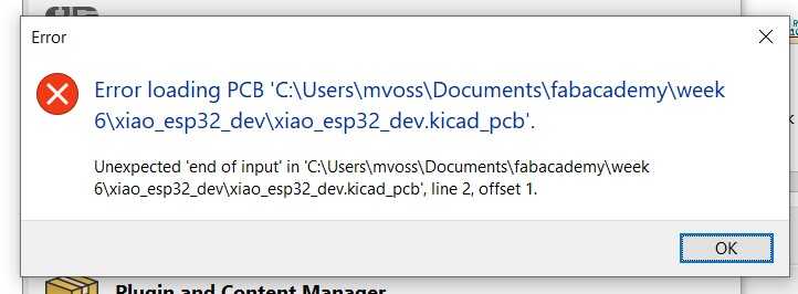
I tried opening the PCB file in a text editor and it was completely empty, so something definitely went wrong. The schematic file was still there though. Luckily this happened after I had uploaded the files to this week’s documentation already, so I could retrieve them from there.
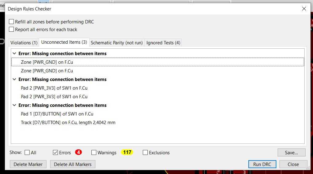
DRC
In week 8 I found out about the Design Rules checker after I realized a part of ground was not connected at all. As you can see in the header image of this week, there is a tiny white line hidden in plain sight between the two areas (under the d in Module on the left). The DRC confirms this. The warnings I could ignore. and some of the errors as well such as the button pads not being connected (doesn’t matter because they are internally connected).
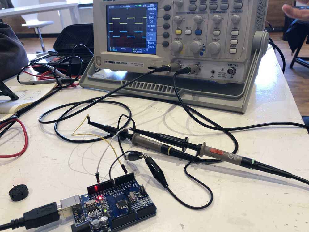
Group assignment
For the group assignment we have to use an oscilloscope and multimeter and document our findings. Erwin showed us how to use the oscilloscope and gave us a ‘puzzle’: figure out on what pins something is happening.

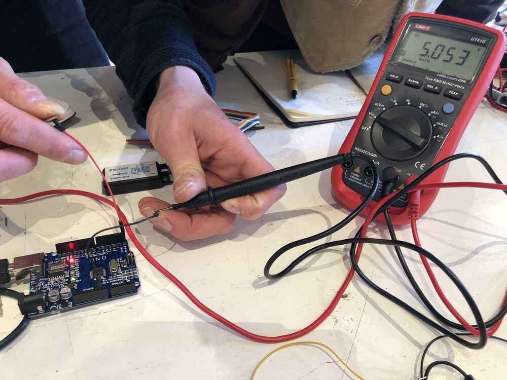
Multimeter
We started by checking the board with a multimeter. First we measured the power pins to verify the oscilloscope was working. The 5V pin and 3.3V should both provide their corresponding voltages. You can see below that that is the case.

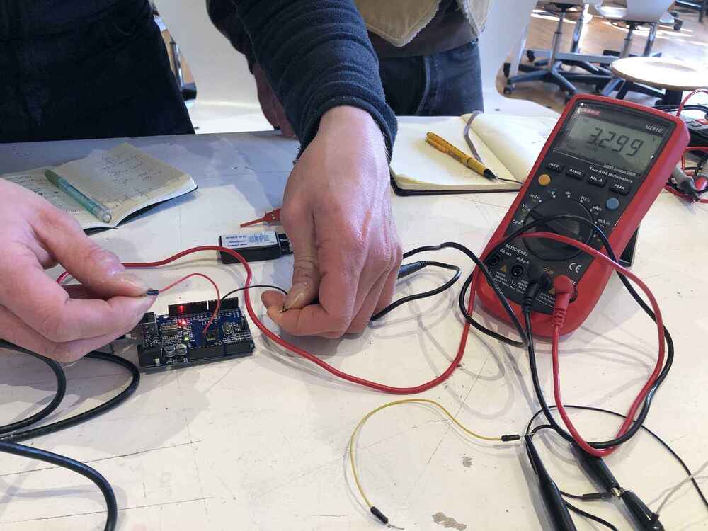
The RX pin is getting a HIGH signal:
We checked the entire board like this with the multimeter; Pieter documented the values measured everywhere.
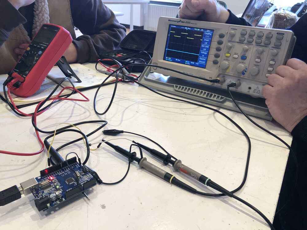
Oscilloscope
Then we visualized the signals with the oscilloscope.
- To measure with the oscilloscope, you need to attach the ground probe to ground on the circuit, and the main probe to the thing you want to measure
- Vertical axis is voltage, horizontal axis is time
- You can set both axes to different scales; under the graph you can see how big one of the squares is in the graph
- With the rotary knobs on the side you can move the signal and scale it independently in both directions to visualize the signal better
- There is a knob on the probe to amplify the signal by 10x so check if it’s set to 1x or 10x
- There are two channels on this oscilloscope indicated by yellow and blue
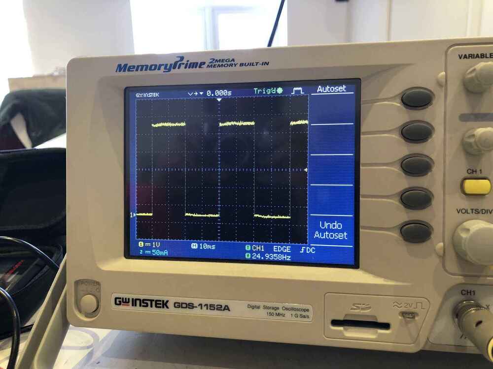
Here we are looking at the waveform of the signal sent to the LED on the board. It’s a 5V - 0V digital signal that is 20ms HIGH and 20ms LOW, so the amplitude is 5V and the period is 40ms which means the frequency is 25 Hertz (1/0,04s). In the bottom of the screen you can see that one square in the graph is 10V high and 10ms wide. The voltage multiplier button is set to 2x which is why the distance between the high and low signals is 10V instead of 5V.
We set the voltage multiplier to 1x and moved the graph around.

There is also an autoset button in the top right corner of the tool. This is often pretty helpful.
Here we connected the yellow probe to pin 2 and the blue probe to pin 13. They both have a period of 40ms: 20ms HIGH and 20ms LOW. While pin 2 is HIGH pin 13 is LOW and vice versa.
If you connect to ground and to yourself, you can see a sine wave. We wanted to see if it was because of the light in the room so we turned it off and on again. The wave seems to move faster but not really. Fluorescent lighting has a frequency of 50Hz which means it turns off and on 50 times every second. This is the same frequency of the mains electricity supply in most of the world (in America and parts of Asia it’s 60Hz).
You see this 50Hz sine wave when you touch the probe when it’s connected to ground because your body functions as an antenna for picking up this 50Hz from mains radiation.
We tried the pocket oscilloscope too; it’s a bit annoying to set up because it only has a couple of buttons to manoeuvre through the menu, but it’s size is charming.

Files
Thursday lecture notes
- Input > System > Output
- Circuit is a closed loop where elctrons can flow from + to - (this is a lie but a useful lie)

- Voltage (V, “spanning”): difference in electrical potential between points, sum of all voltages around a loop is 0 (Kirchoff)
- Current (A, “stroom”) the amount of flowing electrons, sum of all current around a node (knot) is 0 (Kirchoff)
- Power is voltage times current (P, Watt)
- Energy is Power * time (kWh)
-
AC: 230V ~ 0V ~ -230V
- Resistor is a current-limiter, one of the most important components, no polarity; makes sure you have the right amount of current at the right place
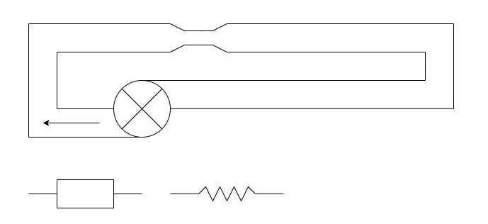

- Capacitor (“condensator”):
- works as an opening and buffer for DC, works as a resistor for AC (you need a coil for AC if you want the DC capacitor effect)
- For DC it’s like a mini tank of water before the circuit continues, the water has to rise enough before the circuit continues
- It costs time to charge a capacitor, the more Farads the bigger the tank
- Electrolytic can charge way more but slower
- Unpolarized are usually quicker but can charge less

- Diodes: one way traffic for electrons, often used as a bridge rectifier = convert AC to DC (see picture)
- LED is a special diode; they are also light sensitive, if you change orientation you can detect light with LEDs (like an LDR)
- Phototransistor is specifically for this just like LDR
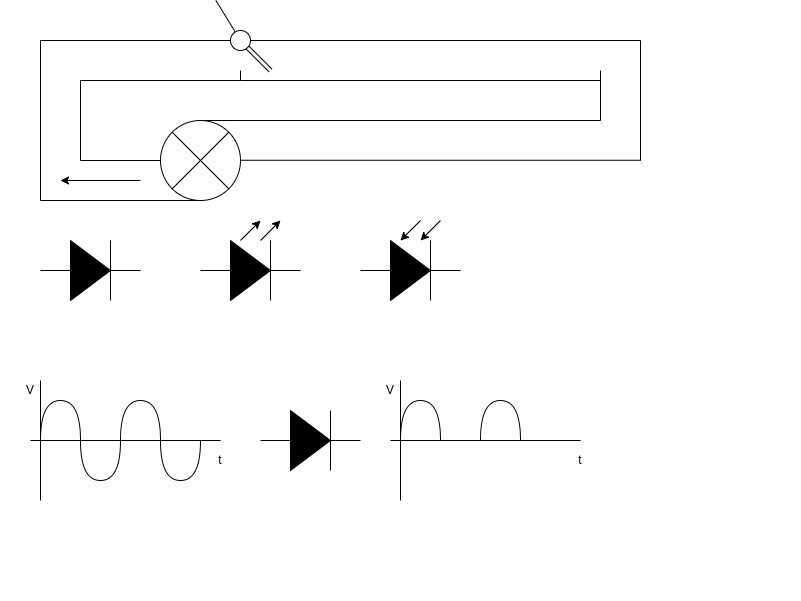
- LED has a forward voltage and forward current
- R = V / I
- if you have a 5V battery and the Vf is 2,1V and the I = 10mA ideally (both in datasheet) you can calculate the resistor you need which is 5-2,1 = 2,9; 2,9 / 0,01 = 290 Ohm
- Bridge rectifier:


- Coil (L, Henry): storage tank for magnetic fields
- used in relays and motors (rotating with magnetic fields)
- flyback diodes used to get rid of the current generated by the magnetic field once you take away the power supply (battery); otherwise you can fry your microcontroller because the current will kind of ‘roll back’ into the microcontroller
- Transistor (Q) is an amplifier and/or switch; a small current can amplify a larger current
- Ic = beta * Ib where beta is the amplification factor (often factor is 100/200); used to amplify audio signals for example
- transistors work with current, mosfets work with voltage
- PNP if you want to put a 0 on the microprocessor, NPN if you want to put a 1 on the microprocessor
- field effect transistor (FET): a small voltage can drive a larger current

- Microcontrollers, integrated circuit built from transistors
- Digital inputs and outputs (I/O)
- Analog inputs (ADC)
- Analog outputs (DAC)
- Digital interfaces (serial, i2c, spi, twi, updi, jtag etc)
Formulas
Ohm’s law
R = V/I in Ohm P = V*I in Watt C = Q/V and I = C * dV/dt; Q is in Coulombs L = V / (dI/dt)
- Capacitance is 1 / (frequency * resistance * capacitance)
- Frequency is amount of changes per second in Hertz If you want it done in 10 milliseconds and the resistance is in the datasheet you can calculate the capacitance 1 / 10 milliseconds / 1/0,01 = 100 Hertz
Frequency
The formula used to calculate the frequency is: f = 1 / T
- f = Frequency
- T = Period
AC is 50 Hertz so it changes polarity 50 times per second.

Tools
Multimeter is the tool for many things, so voltage, current, resistance etc
- Make sure to switch back modes after you are measuring current! Otherwise you can short your circuit or the multimeter
Oscilloscope
- Most versatile measurement tool; multiple voltage in time domain, frequency counter
- There are also PC based (with DAC) oscilloscope
Logic analyzer: only for digital signals, helps to interpret what digital signals mean Logic 2
Lecture notes
I followed this lecture two years ago and documented all of the component Neil talked about. This is what I wrote down with some added notes:
Wire
- Ribbon cable: when you need a multi conductor cable and connectors that clip onto it; and we use it as hook-up wire (peel it off)
- Awg (american wire gauge) wire current tables for information on your wires (diameter, resistance, current etc)
- You need a wire that is thick enough for the current you’re carrying, otherwise it will overheat
- Wire with solid core (low frequency) and wire with strands (high frequency)
Button
- Push button: when not pressed it’s open, it closes the circuit when pushed (2 legs on opposing sides)
- Slide switch: stays where you leave it (open or closed), center conductor and 3 side conductors (used for on/off buttons often)
- Resistor: specified by a resistance value (I = V / R). There is a current flowing through the resistor > there’s voltage drop across the resistor, and the change in voltage equals current * value of the resistor (they have max. power that they can take before overheating, and tolerance for errors). We use resistors to control current (current limiting) most commonly, or for timing
Capacitor
- Capacitance (C = Q / V, V). There is charge on it; it stores charge, there is an electric field in it. The rate of change of the charge equals the current (Current is proportional to the rate of change of voltage for a capacitor). Vdot proportional to I
- If the voltage is constant/steady, nothing goes through, but if the voltage changes quickly, something comes through > AC goes through, DC is blocked
- Farad is the unit, max. voltage is important to note
- There is polarized (bit more complex, stores energy and can be used as an energy source to quickly charge for example a toy) and unpolarized capacitors (unpolarized are the ones we use)
- A capacitor ‘cleans up’ noise in the voltage between power and ground
- A bigger capacitor near your component stores a little bit of energy (acts as a battery) when you switch it on
Crystals and resonators
- A capacitor with a material on the inside, with voltage on it it flexes, like pushing a swing (oscillating)
- Can be used to tell time
- Unit is frequency
- Internal clocks in processors are now good enough to use for most purposes, only need to use them if timing is very precise
- Resonators are cheaper
Inductors
- V = L * Idot
- DC goes through, AC is blocked
- Blocks high frequency noise
- Inductors and capacitors can oscillate together, for filters or interfacing radios
- Less used compared to other components
Diode
- 2 sides, anode and cathode, a > c (mnemonic: alphabetical order), + > -, long leg to short leg for tht components
- Can use it to block a signal (or stop you from frying your board if you connect it the wrong way I think)
- Diode drop > prevents current from going backward
- In the forward direction: past the diode drop it’s essentially a perfect conductor
- The dent/dot/etc is always the cathode side
- You can use a Zener diode to clamp a voltage (when you don’t want it to go above a certain voltage), useful is you have a 5V power supply and a 3V chip
- LED is a diode (always check the spec sheets for brightness, color, max voltage etc, you need a resistor for this weeks assignment, typically 1kOhm otherwise you could literally blow up the LED)
Mosfet (transistor)
- Gate, drain and source
- Parameters we care about: max. current it can handle, rbs (resistance between drain and source, you can look at the graphs for this)
- You can loosely think of this as a switch (it’s actually continuous), as you vary the gate voltage, the gate is controlling the value of the resistance between source and drain; generally all the way on or off and then turns on and off quickly (with intermediate values you dissipate power > HEAT). We use it to switch current
- https://circuitcellar.com/research-design-hub/transistor-basics/
- Different types of mosfets and transistors (transistor wise we are only using mosfets)
Power supply
- Batteries or USB, DC and AC
- You need regulators to work with the processors (to go from X Volt to for example 5 Volt). *You need a difference to regulate! Otherwise the regulator doesn’t have anything to regulate
- Buck and boost regulators > not using those
Op-amp
- Output is (input * output) * huge multiplier (a million or something), to amplify a signal
- Spectacular specs
- Neil loves them
- We will sadly never see them usually
- Microcontrollers we use have them built right into them so we usually don’t need a separate one
- You could use them to interface to a microphone, or if you need very sensitive filters (you could also make software filters if it’s not that sensitive)
Microcontroller
- Basically a small computer
- Example of integrated circuits (all the components are hidden inside)
- Designed to perform a predefined task (you give input, the controller gives an output) that you program it to do. It has no working memory so you can’t store anything on it, and there’s no operating system on it.
- You need to understand the datasheets!!! Read them, there’s so much going on in a 1 dollar piece, it’s amazing
Designing circuits
- Kirchoff’s law: all your voltage going in has to go out (total is 0 unless you’re charging something)
- Power = I^2 * R = I * V
- Wherever possible we want voltage drop to be low and resistance to be low (less heat)
- EDA: electronic design automation
- Designing PCB’s needs to be hierarchical and parametric (because of trace size, package size etc)
- Footprints: the bits where you connect the components; they come from part libraries
- Processor: dot goes on the little longer footprint to help with the orientation
- Routing the traces (autotraces don’t always work for small circuits)
- Simulate before you make it
- Your design has to respect your machine’s design rules
- You can also draw one by hand (nice to try out, not recommended)
- Rat’s nest: not routed yet
PCB Design Tools
- Fritzing, TinkerCad, Virtual Breadboard: nice for learning but we’re not going to use them
- LibreCad, EasyEDA: options, open source
- Eagle: also good option, great integration with Fusion360, however it’s not free and open source, but it’s integrated in Fusion360 license
- KiCad (free, open source and cross platform): we are using this one
- OrCad, Cadence (1 million dollars to set up the installation), Synopsis: higher end PCB design
- Magic is an open source tool also with integrated circuits
Kicad
- Very powerful
- A bunch of separate programs so that makes it harder to go back and change something
- Wire up the resistor to the processor
- Open the tool and tell the value of the resistor and which package for the processor we use
- Produce net list: who is connected to whom
- Open PCB tool, bring in net list
- Start routing (takes quite some time): connect the components (push routing: helps with routing)
- Edge cut: defining the boudary of the board (there’s a 3d viewer in KiCad)
- Export layers (multiple formats available): we export images for mods (SVG, white is high and dark is low, so we have to invert the svg)
- Mill it
Libraries
- Logical representation of components in libraries
- Vendors want you to use their parts so they work on great library sources
- We use the fab library mostly
SVG PCB
Simulators
- There’s very expensive high end simulators for very expensive chips
-
Fahstad.com in browser simulation is really cool
- Verilog: hardware description languages, expressing algoritmic relationships (not recommended for beginners)
- PCB.py: functional representation
Digital oscilloscope: logic analyzer, great tool for debugging, 300 dollar, looking at signals