Electronics Design
Assignment to be done:
1.Group Assignment
Use the test equipment in your lab to observe the operation of a microcontroller circuit board
To be found here
Relection of what I learned from group
First of all, from my group I knew that test equipment are instruments used to measure, test, and diagnose electronic circuits and devices.
From these equipment we can test different quantities such as current,voltage, power, resistance, continuity etc.
Among equipment we have used I can say:
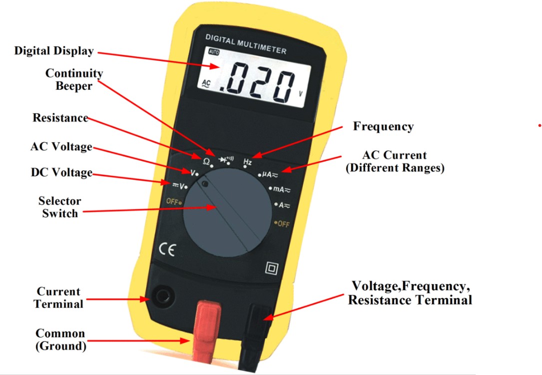
1.Multimeter:used to measure voltage, current, and resistance, etc as it has different ranges to calibrate any quantity you need to test/measure. They are two types of Multimeter which are analog and digital
2. Oscilloscope:is an instrument used to measure and display electrical waveforms, such as voltage or current signals, over time. They are also of two types that are analog and digital.
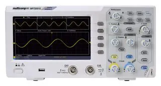
Fig: Digital Oscilloscope
. Design a development board to interact and communicate with an embedded microcontroller
. Extra-credit:Try another design workflow
. Extra-credit:Make a case for it
. Extra-credit:Simulate its operation
Individual Assignment:
Design of a development board to interact and communicate with an embedded microcontroller
Whta is development board?
A microcontroller development board is a type of development board specifically designed for prototyping and experimenting with microcontroller-based projects. A microcontroller is a small computer on a single integrated circuit that is designed to control electronic devices, and is often used in embedded systems. A microcontroller development board typically includes a microcontroller chip, power regulation circuitry, and various input/output interfaces such as USB, UART, SPI, I2C, and GPIO pins. It may also include additional components such as sensors,displays, and motor drivers,etc to enable a wide range of project applications. Reference from here
How to design a development board of Microcontroller?
Here are some basic steps:
- 1. Choose and have the software to be used
- 2. Select a microcontroller that is suitable for the project based on different requirements such as the number of input/output pins, processing power, memory capacity,interface compatibility, etc
- 3. Apart of microcontroller, identify the components that you need to use
- 4 Create a schematic circuit that shows the connections between the components and the microcontroller.
- 5. Design the PCB from designed schematic circuit by placing the components on the board, routing the connections between them, and adding ground and power planes.
- 6. Once the PCB design is complete, use milling machine to fabricate the board/PCB
- 7. After milling the PCB, solder the components on it
- 8. After soldering all the components on board, check if there is any error by measuring like a continuity etc by using multimeter
- 9. Use an integrated development environment (IDE) to program the microcontroller. Sometimes You may need to install drivers for the microcontroller and any peripherals.
- 10. Connect the board on computer for power source and uploading the codes into microcontroller and test its functionality.
- 11. If any issue arise, debug by making any necessary modifications to the board,components or code.
Designing a development board
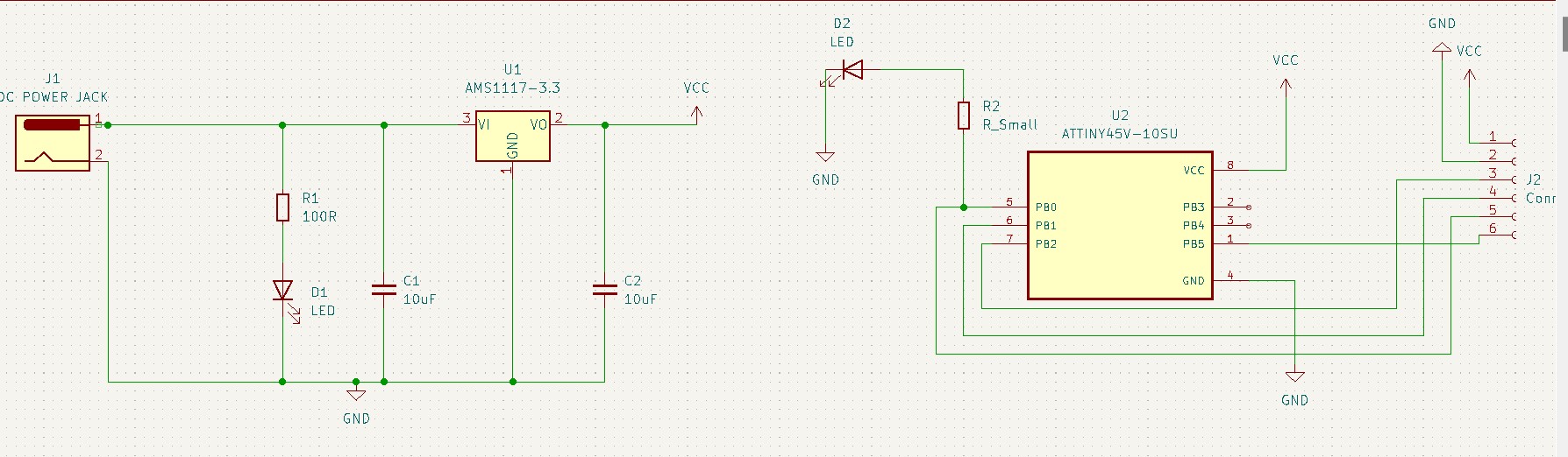
The chosen microcontroller to be used in this work is ATtiny45 Microcontroller
The Attiny45 is a microcontroller chip from the Atmel AVR family, which is a low-power, high-performance microcontroller architecture. It is designed to be small and efficient, making it ideal for use in embedded systems and other applications where size and power consumption are important factors. The Attiny45 has 4KB of flash memory for program storage, 256 bytes of SRAM for data storage, and 128 bytes of EEPROM for non-volatile storage. It also has 6 I/O pins, including 3 analog input pins, and can run at clock speeds of up to 20 MHz. The Attiny45 is programmed using the standard AVR programming interface, which can be done using a programmer such as the AVR ISP or through a bootloader. It can be programmed using C or assembly language, as well as higher-level languages such as Arduino. The Attiny45 is a versatile and cost-effective microcontroller chip that is commonly used in a variety of embedded systems, including robotics, home automation, and industrial control systems.
For more about datasheet and architecture of ATtiny45 Microcontroller you can refer from here

Fig:ATtiny45 Microcontroller
ATTINY45 is high performance, low power controller from ATMEL. It is an 8 bit controller based on Advanced RISC architecture. It is one of members of ATTINYXX series, popular because of its small size and features.
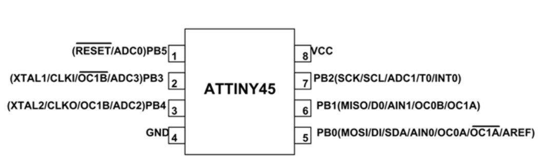
Fig:ATtiny45 Microcontroller Pin out
To design the schematic diagram and pcb, I used the KiCad and I started downloading it from here.
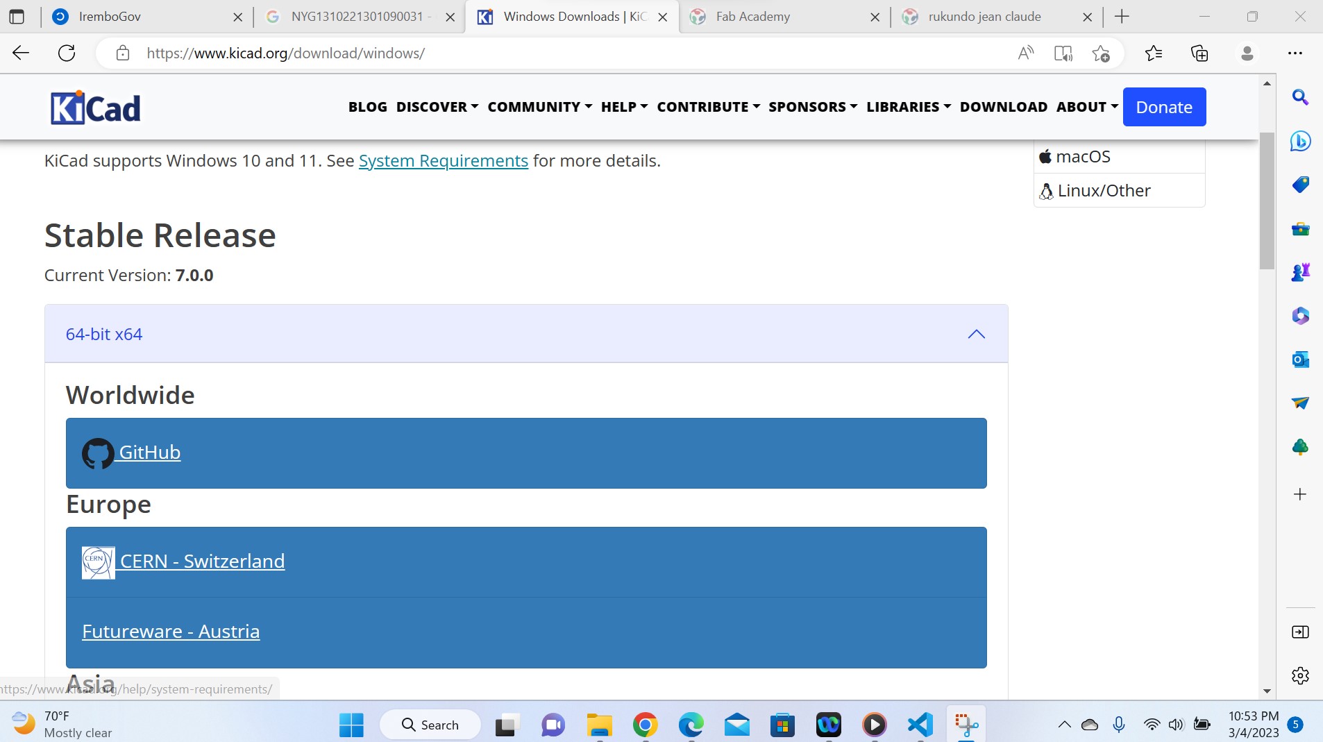
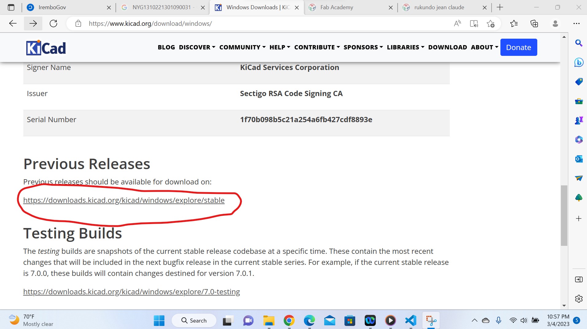
Fig: I chose the previous release which is version6 from this link hoping that it is the one I can be familia with quickly
Then after downloading the Kicad, the next step is to dedign the schematic diagram or the circuit starting on regulated power supply circuit as all electronics ciruit should be suplied by the regulated power.
Procedures to design the schematic circuit and PCB
1. Opening a Kicad and creation of a project,name and save it

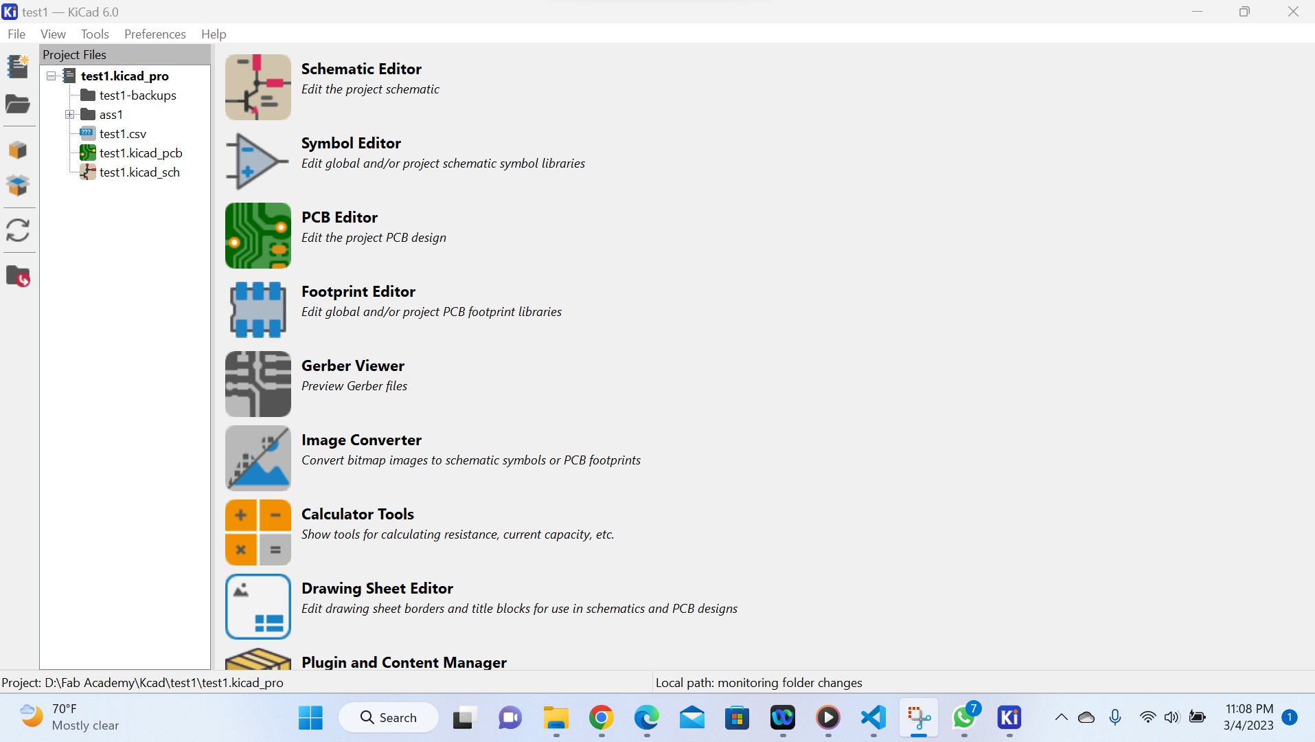
Fig:Starting the Kicad software for PCB design
After creating and saving a new project, you open it and start designing your schematic circuit
2.After opening the working space, you import all components you will need for designing your circuit
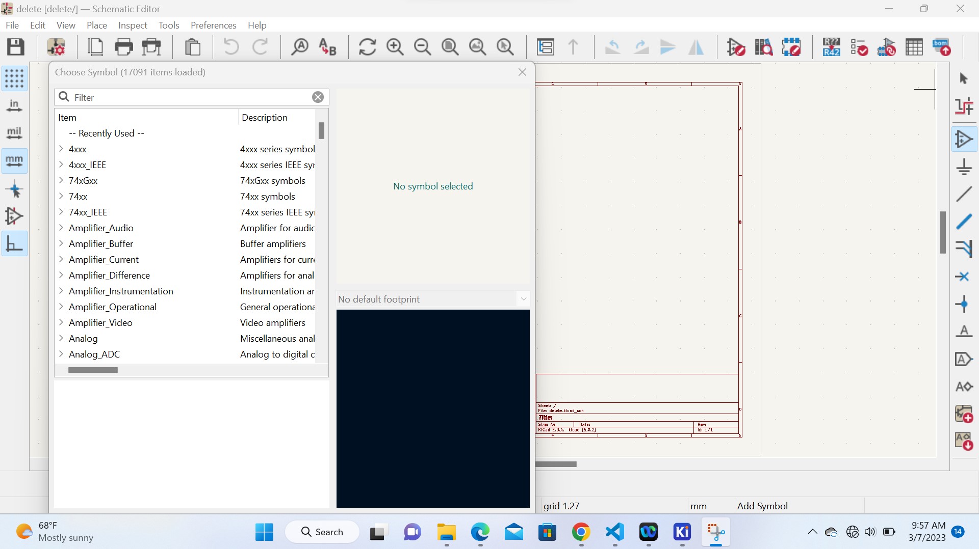
Fig: Here you choose the components according to your circuit.
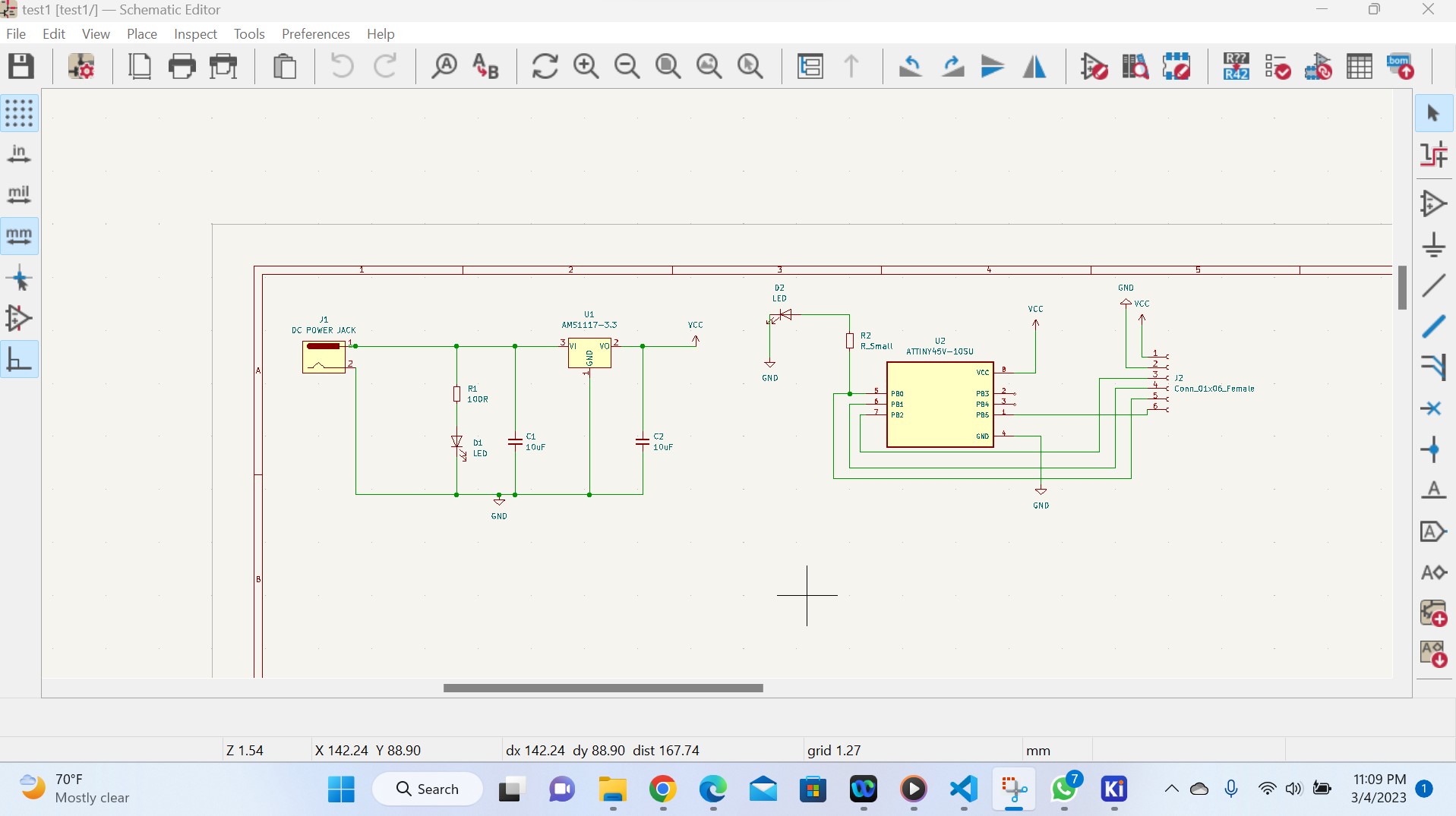
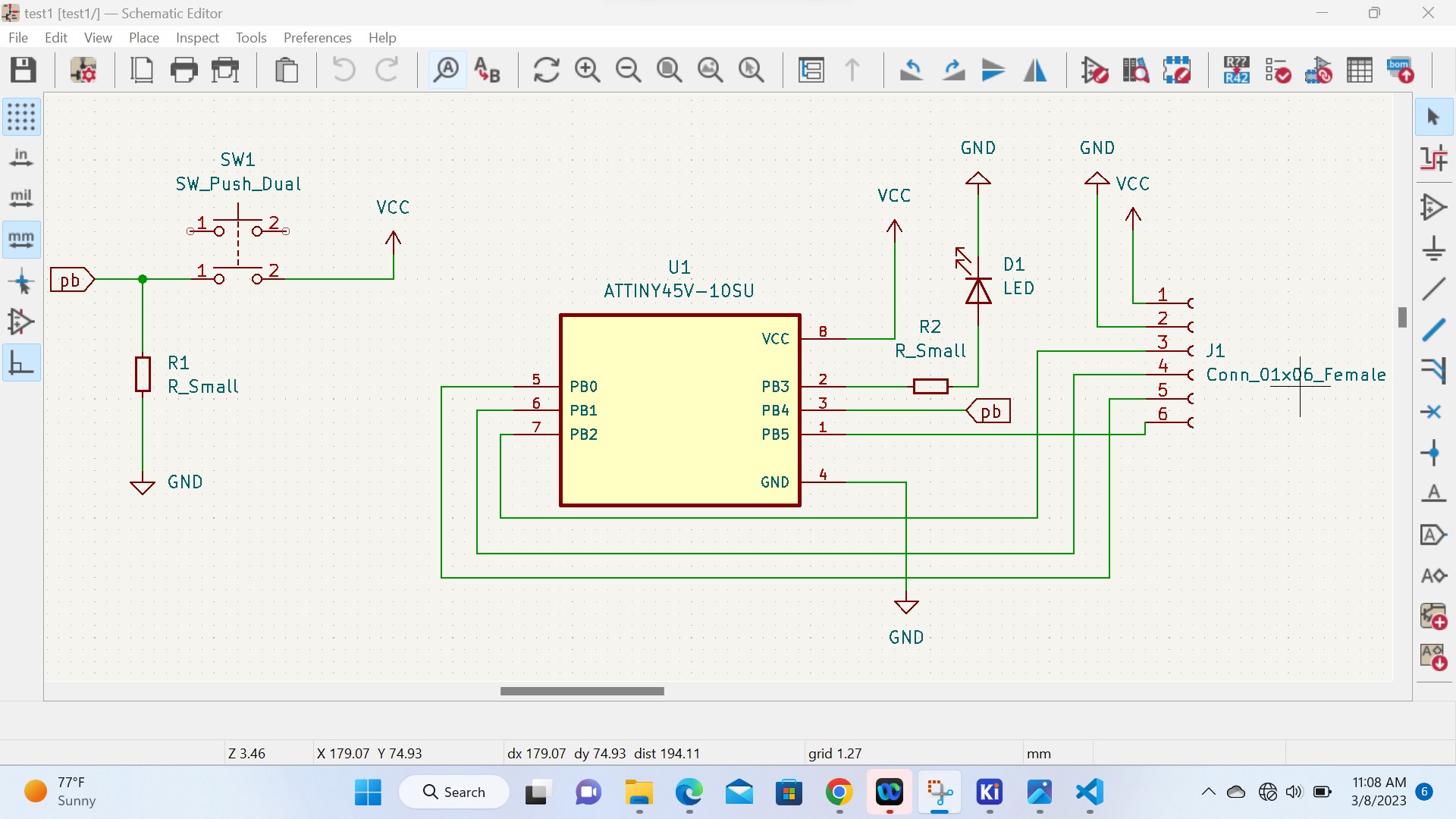
Fig: Schematic circuit of board development
3.After designing the schematic circuit, you Create, edit and assign or delete a footprints to each component you used
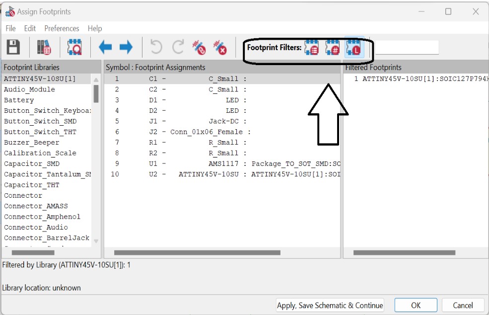
4. The next is to annotate: annotation refers to the process of assigning unique identifiers or labels to different components, nets, or nodes in a circuit diagram
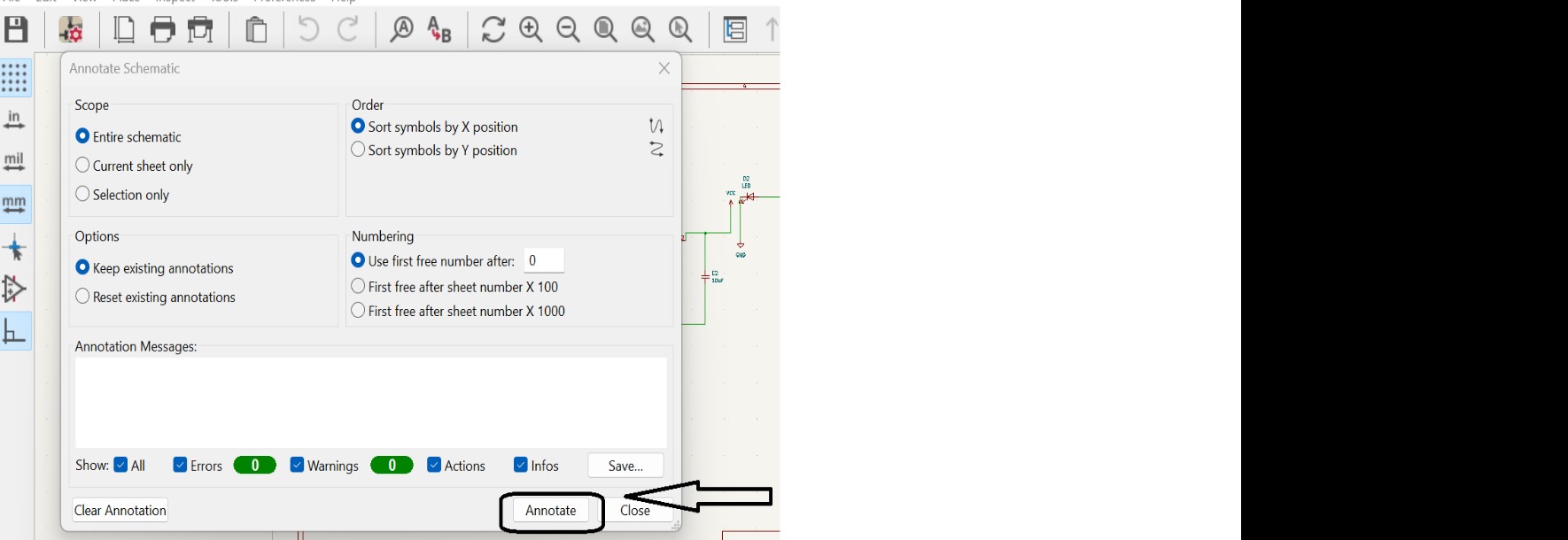
After you perform Electrical rules checks : such as unconnected,violations,errors and warning
Here you check different errors/mistakets you committed during design of your schematic circuit. if exist, you rectify them. So the circuit down here is the final design of schematic diagram of my project.
Setting up the design rules for my PCB
Defining board design rules with the goal of ensuring fabrication and assembly yield refers to the process of establishing specific guidelines and constraints for the design of printed circuit boards (PCBs).
These rules are implemented to maximize the likelihood of successful PCB fabrication and assembly, ensuring that the final product meets the desired specifications and functions correctly.
Fabrication yield refers to the percentage of PCBs produced that meet the required quality standards. Assembly yield, on the other hand, pertains to the percentage of PCBs that can be successfully populated with components and function properly.
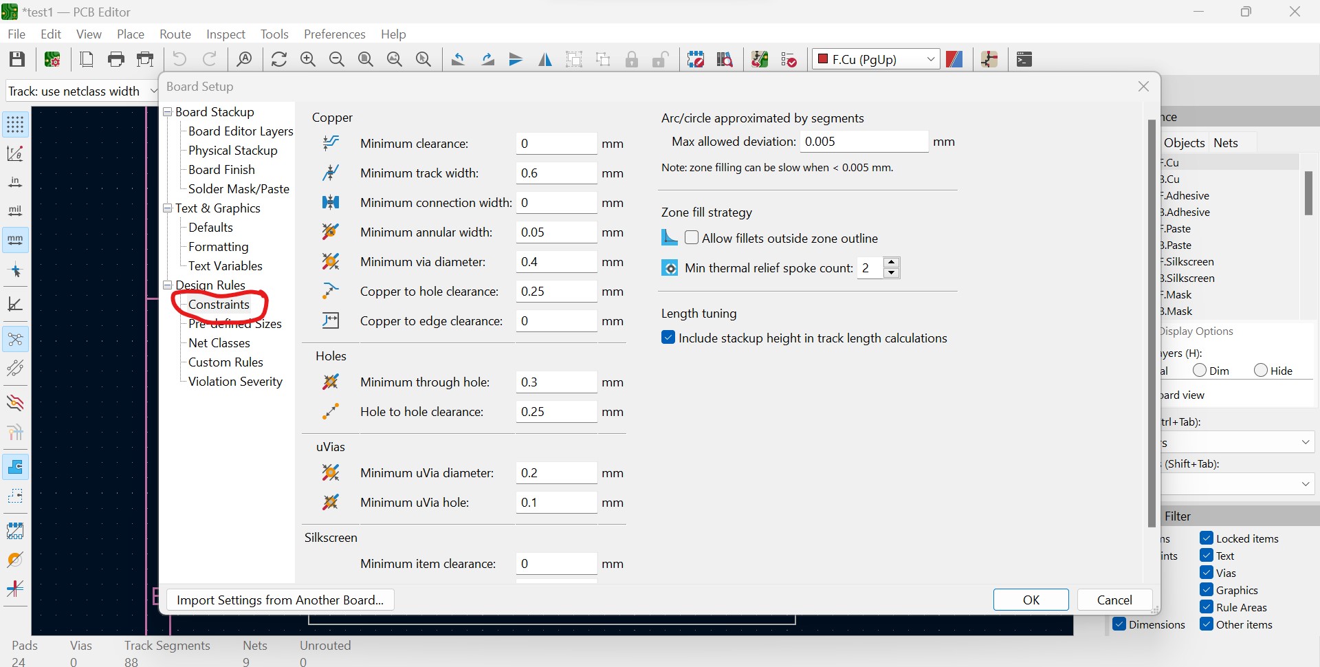
By defining board design rules, PCB designers aim to optimize the manufacturing and assembly processes, minimize errors, and increase the overall yield. More details about design rules in general and note that for me I used KiCad and down are the design rules I used.
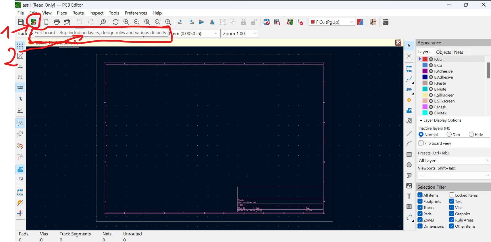
In KiCad, to set the design rules, you click on edit board set up and customize the boar's parametters as you wish as here highlighted on the following photo

And you can see that with the above photo, in board set up, I'm using two signal layers
constraints: Bellow photo shows how to set constraints: of the board under design rules
Net Classes: with net classes, you can customize, track width, clearence, via hole, via size etc, as shown in the following photo:
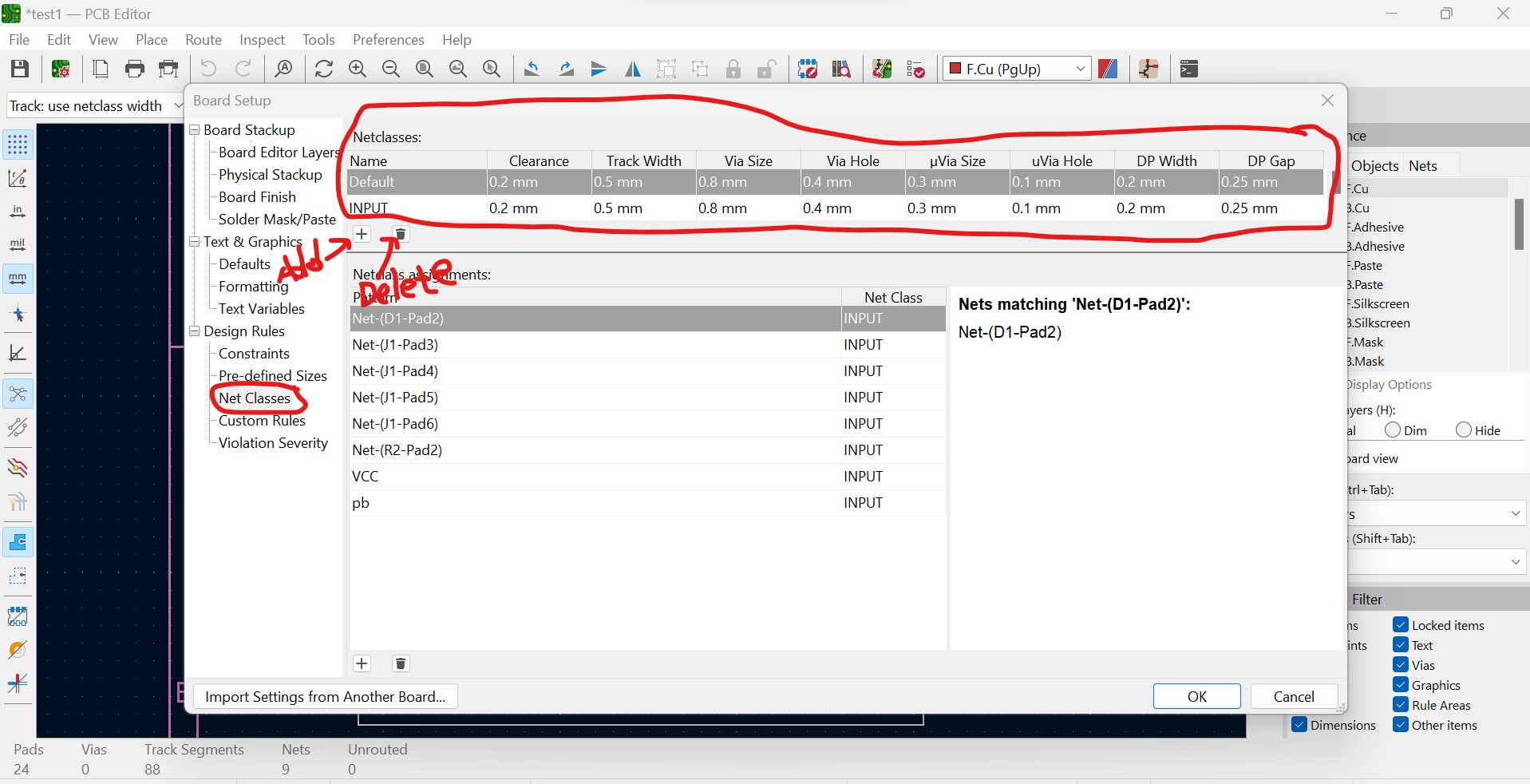
here you can add as well as delete the input(layer signal).
For more information about the design rules in KiCad please refer to Design rules in KiCad
Note that I used KiCad version7
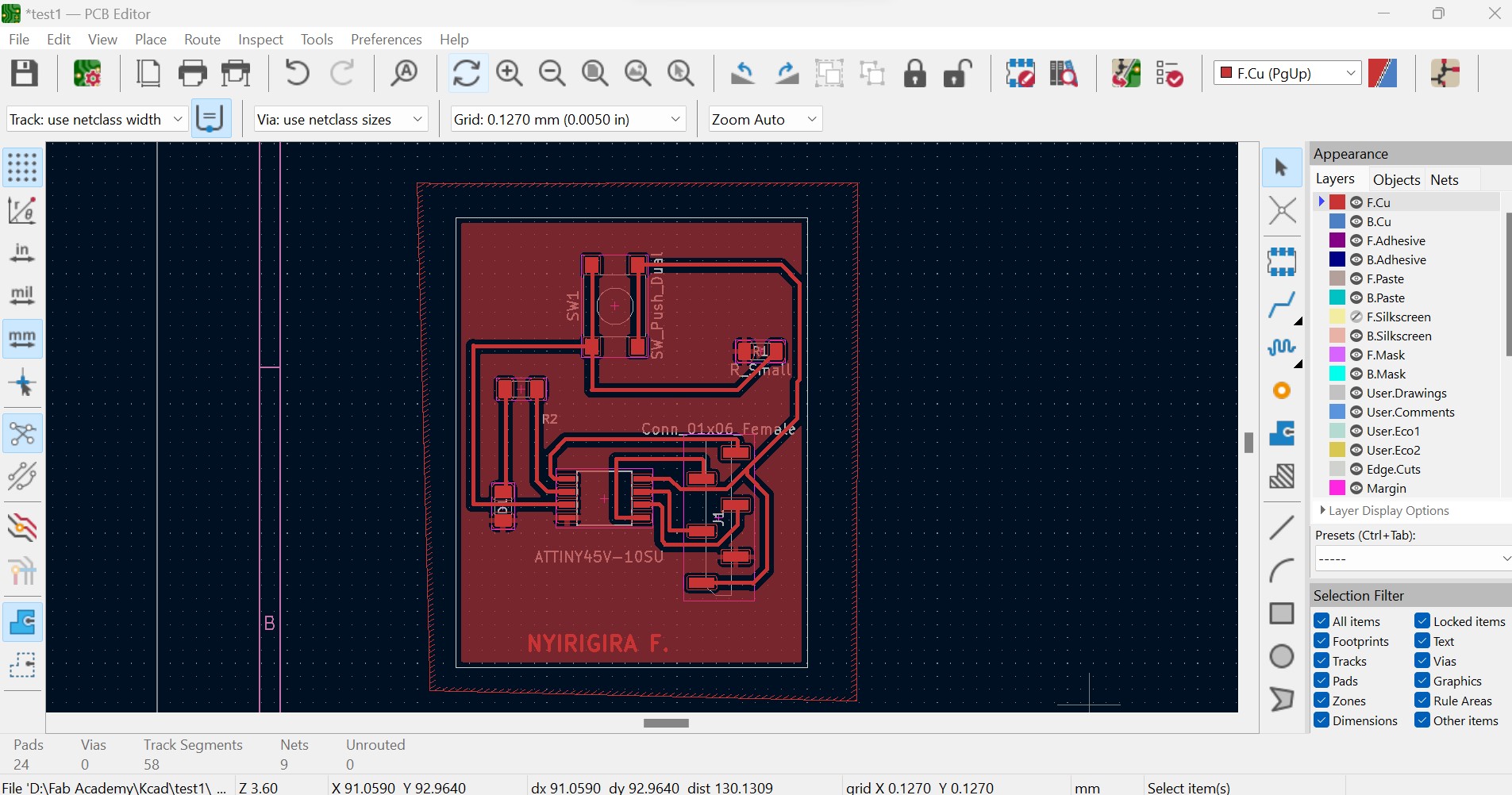
Down here is the PCB layout of the designed schematic circuit of my project.Actually this layout shows how the circuit will look like after being printed on PCB, It is normally the PCB which is the printed circuit board.It will include the fixing of the components on the board and routing traces between them, mounting the holes, board edges, and among others.

Fig:Footprint of the board development

3D view of the designed project, here shows the physical or real view of the project after being printed out.
The above was exercise 1, then down here is the second exercise I have done with its smulation shown with the video at the end of this page
Schematic diagram or circuit of the system
The following is the Footprint of the designed circuit
3D view of the components on PCB:

After finilizing the design of PCB, I exported it and saved it as svg:


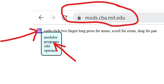
And after all designs, we transfrom the designed pcb into G-code through https://mods.cba.mit.edu/ G-code is a programming language used to control computer numerical control (CNC) machines, such as milling machines, lathes, and 3D printers. It consists of a set of instructions that tell the machine how to move its tool to create a desired object from a raw material.

connecting input and output files and setting the X,Y,Z origins:
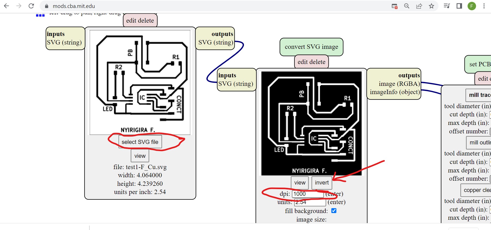
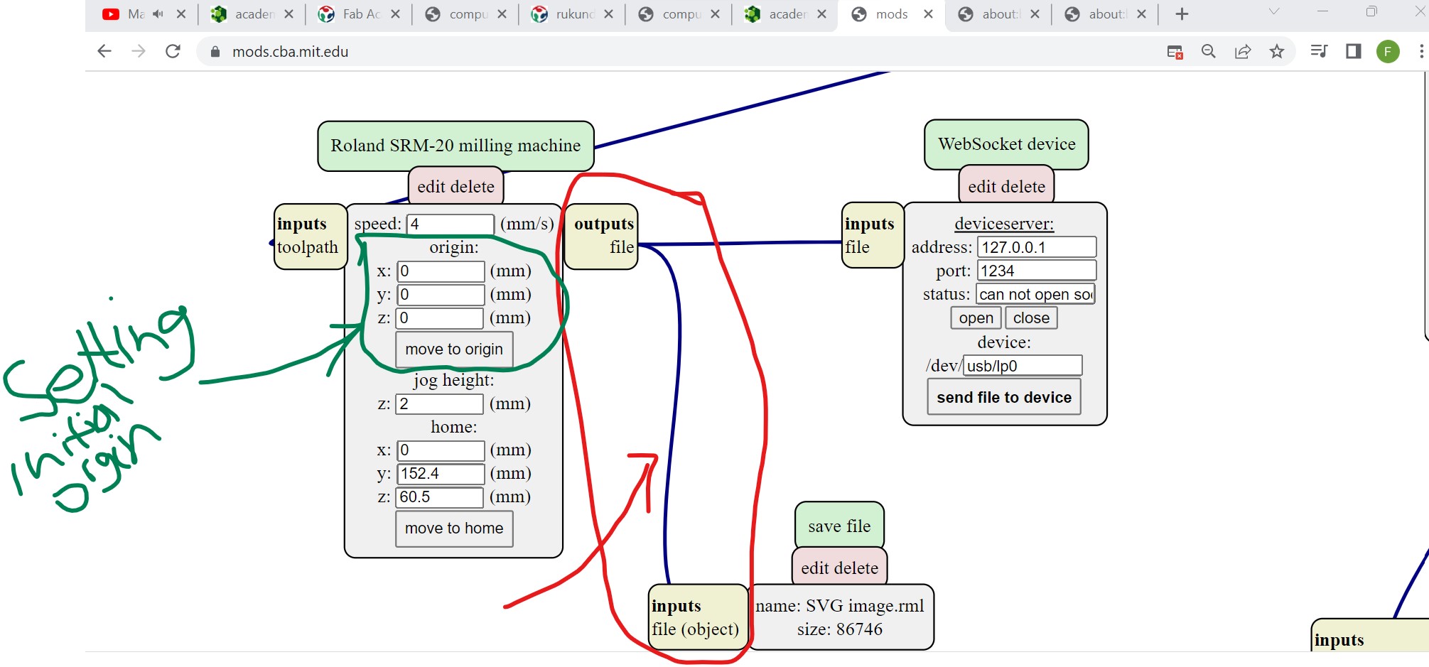 After connecting, upload the designed PCB file by clicking on select svg file, set the dpi you want to operate on(here I chose 1000) and invert the uploaded design to see where the milling machine will trace.
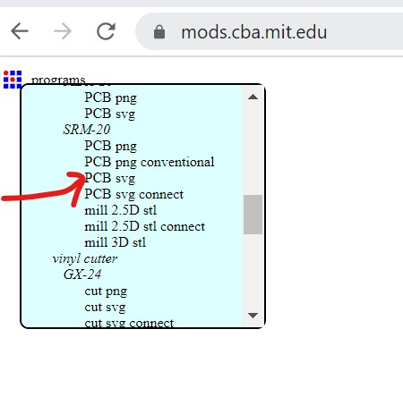
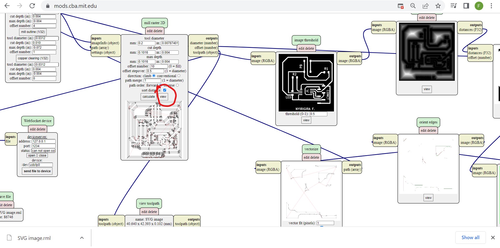
 After uploading and invert an svg file, you set the pcb defaults by clicking on mill traces and mill raster 2D parameters. Here I setted the used tool's(drilling bit) diameter which wa 0.2mm and offset number as 10 as turns to engrave the traces on pcb.
After those settings just click on calculate and de file to be milled downloaded immediately as it is shown in downloads folder.
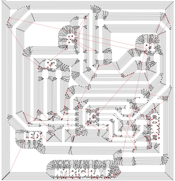
Then you view the Footprint of your designed pcb
Note that the downloaded files is for front view where the traces of connecting the components are to be engraved, the next is also to set the parameters
of the out cutter where the pcb will be cutted off. Actually the procedures remain the same except clicking on mill outline instead of mill traces and changing some parameters like I changed the tool diameter on 0.9mm as the size of drill bit I used, off set numer at 1 because I wanted the drill bit to
pass once into trace while cutting as shown in the following photo

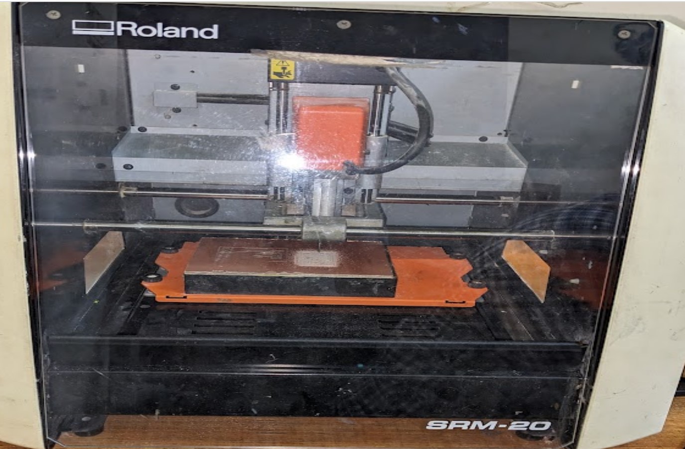
The next step is milling a PCB by using milling machine as shown in the following pictures:
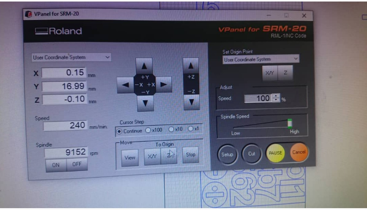
Fig: Control software for SRM-20. Setting axis and uploading G-codes
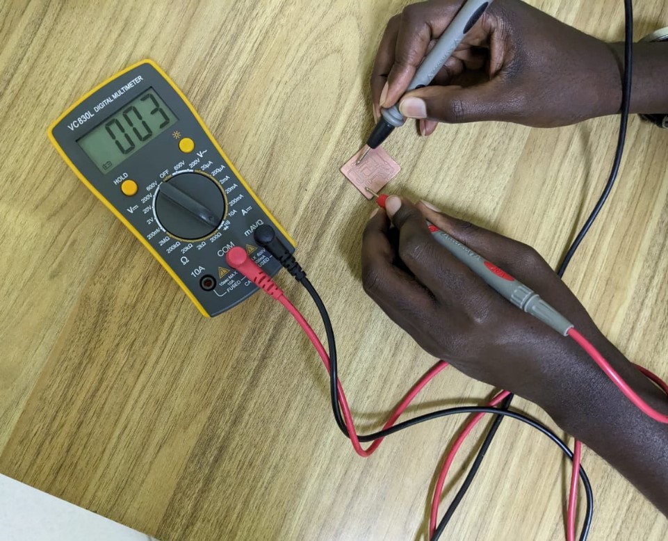
Testing the continuity between the traces on the PBC after milling:
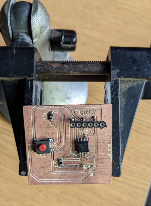
After choosing the physical components to be used, I soldered them on milled PCB by using soldering iron and soldering tin as illustrated below

Image below shows the PCB with soldered components afeter soldering process.
Connecting my ATTINY45 board to an other Microcontroller
After getting my board ready, I connected it to Arduino for communication. Here what I need is spi communication and I use MOSI,MISO and CLK pins of ATTINY45.
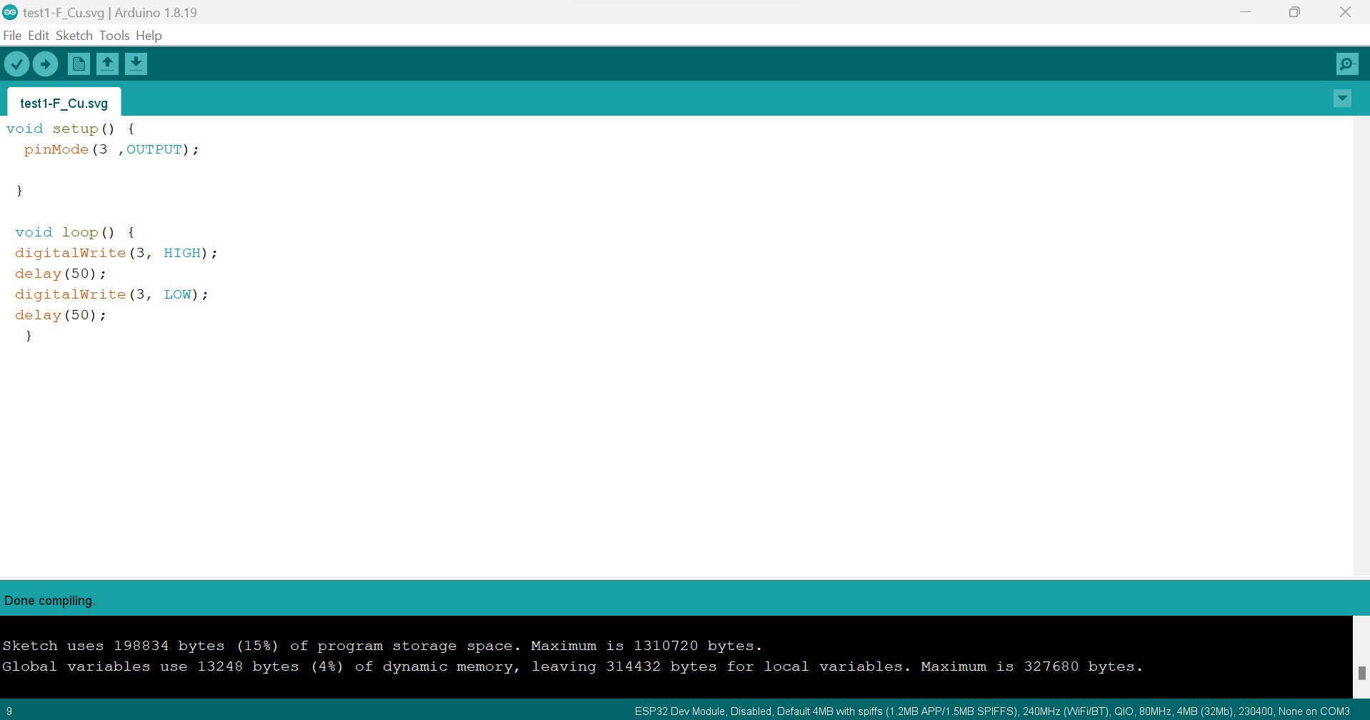
To be sure that it works, I just programmed it in Arduino with the following codes to blink a LED and as shown in the the video at the end.
            void setup() {
               pinMode(3 ,OUTPUT);

              }

              void loop() {
              digitalWrite(3, HIGH);
              delay(50);
              digitalWrite(3, LOW);
              delay(50);
               }
All those works(designs) done in Electronics Design have been saved as files and they can be accessed and downloaded as a whole zipped folder via here
NAVIGATION
USEFUL LINKS FOR MORE KNOWLEDGE
https://randomnerdtutorials.com/ https://www.w3schools.com/java/java_intro.asp https://www.w3schools.com/html/default.asp https://developer.mozilla.org/en-US/docs/Web/HTML/Element/brAddress
2023 All Rights Reserved. Designed by Felix NYIRIGIRA