6. Electronics design
This weeks topic was electronics design. As a group, we were to use the test equipment in the lab to observe the operation of a microcontroller circuit board.
We documented our work to the group work page which is on our Fablab Oulu pages. Check out our results!
Reflection
In embedded programming week we used the oscilloscope to define output frequencies from our developer boards. We tried to also measure power consumption, but our testing equipment wasn't up to it. We decided to try that again this week when we had another equipment and decided to measure it with RP2040.
The RP2040 is known to have low dynamic power consumption. As expected, with our small testing, we found out that the tasks were using very little power. First we connected the RP2040 to computer, and in Arduino chose to use it and defined the port. Before running any code, we checked the readings. It was under 30 mA.
The MCU was plugged in, but it's not operating any code. So what is happening in the MCU when it is connected? I used a guide to help me out with this.
It was explained in the guide that the common terminology for the process when a microcontroller is powered up is called the ‘boot process’. For a computer, booting refers to the process of turning a computer on and starting the operating system. In a computer the operating system is the program that enables the software and hardware to work as one.
For a microcontroller, what happens when it is powered up is a similar process. However, microcontrollers do not come installed with an operating system. The operating system is the list of instructions you write (the ‘program’) and load onto the microcontroller.
So, if the micrcontroller’s reset button is pressed (which is essentially resetting the system), the boot loader carries out the same task of loading program code and other essential data. When we connected RP2040 to computer and opened Arduino, we needed to press the Boot and Reset -button for it to be recongnized. So the boot process had been done and the first measurements were taken in this point.
After that we run a couple of codes; one blinking the small LED and other blinking different colors on the RGB LED. The power consumption was low throughout our tests. In blinking different colors with the RGB LED it varied a little according to the color.
Individual assignment was:Design a development board to interact and communicate with an embedded microcontroller
Learning outcomes:
Design a development board
We were explained the pros and cons of designing with KiCad and Eagle. KiCad was chosen to be the designated designing program this week, and we were suggested to test out Eagle too when we have time.
Adding libraries to KiCad
I downloaded and installed KiCad. We were asked to download the fab library from gitlab. The library covers all the electronics components found in the official fab inventory. The instructions were good, no problems there. Then I needed to point to the library in KiCad so I opened it.br> In Preferences -> Manage Symbol Libraries -> add fab.kicad_sym as symbol library.
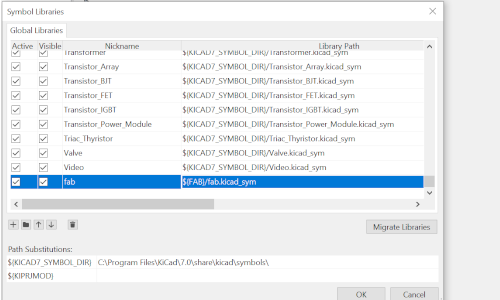
Then I added the footprint library in Preferences -> Manage Footprint Libraries -> add fab.pretty.
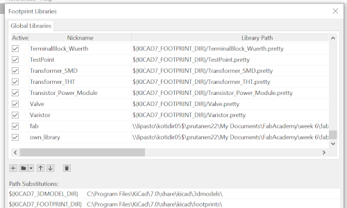
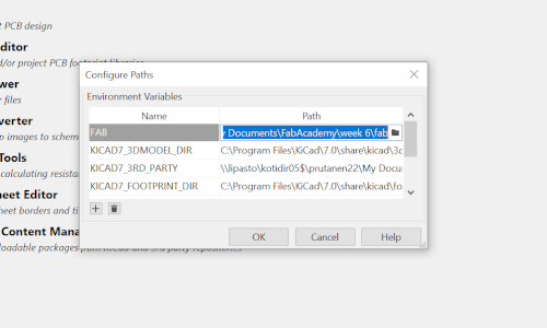
I also added one file from our instructor to the library directory which was called own_library.pretty and was a kicad mod file for XIAO socket we would need later on. Then in Preferences -> Configure paths I added the path for fab.
Now everything was set up for the project!
Starting with Schematic editor
Our instructor showed us a board that was made before. It was a beautiful looking board that had for example a button and a LED beside the RP2040.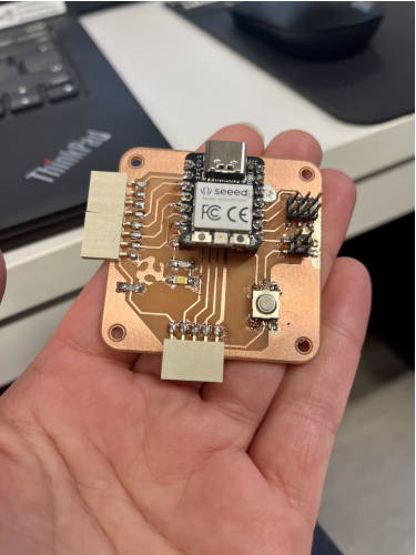
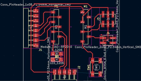
I opened File -> New project and named it First Design as nothing else came to my mind. I opened the Schematic editor that was created under the project. Our instructor showed us how the board in the photo was designed; what did it have in it and how were the parts laid out.
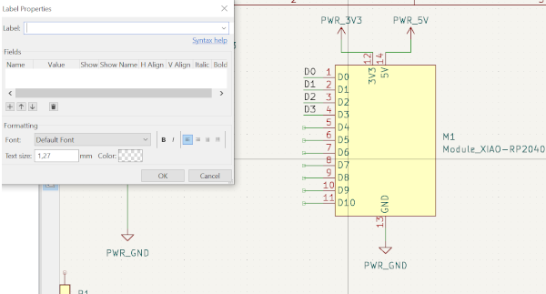
I started to look out for the parts. When I pressed the Add symbol button on the right of the page, it opened a window where I could choose a symbol. But there were over 19 000 symbols to choose from so this made my head spin at first! I wrote in fab and saw Pin headers at the top of the list. We were to find a single row male connector with 8 pins with size on 2.54 mm. I found it, chose it and dropped it into the schematic. The next one I searched for was the LED and a resistor.
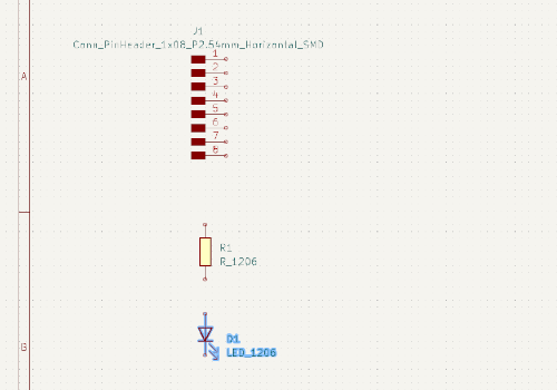
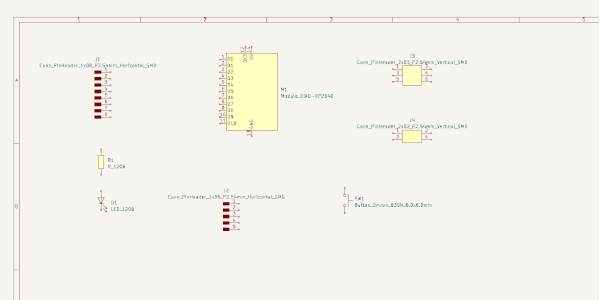
There was another male connector of 5 pins, button of 6x6mm, connector header Surface Mount 4, connector header Surface Mount 6 and then of course the module XIAO RP2040.
Then I had to bring in enough powers (PWR_3V3 and PWR_5V), grounds (PWR_GND) and also PWR FLAF which tell ERC where the power signal comes from. The next step was to start connecting all of these symbols with wires. With the designed board sample I knew what had to be brought in together. I just pressed Add wire from the tools on the right, and clicked the parts to be connected.
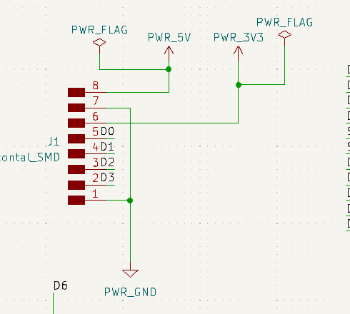
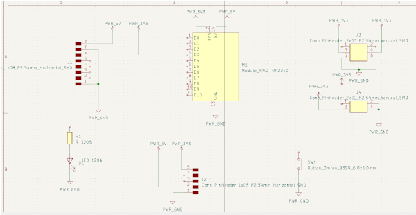
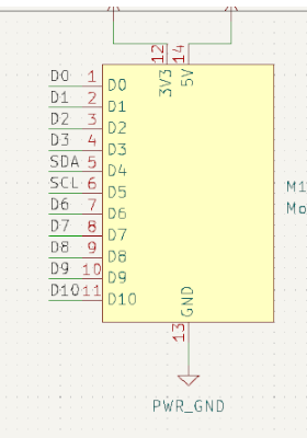
Then I started to add labels in Place -> Add label. I made short wires to the symbols to easily attach the labels. In the module SCL means serial clock pin that the Arduino Controller board pulses at a regular interval, and SDA means serial data pin over which data is sent between the two devices. The XIAO RP2040 designates package pins 5 and 6 to be SDA and SCL.
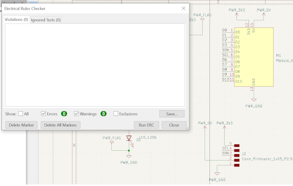
Then it was time to do check-up with Perform electrical rules check- button on the upright panel. When I pressed Run ERC, no errors appeared.
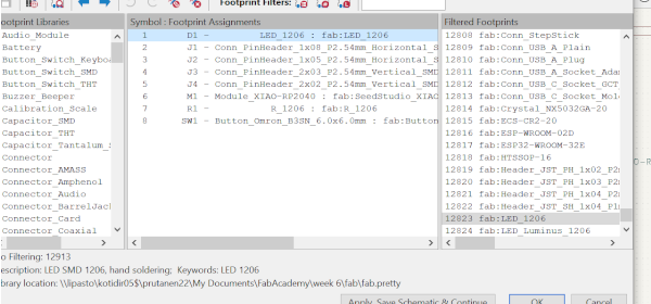
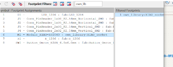
There was one thing left to do; to check for the footprint assignments. We knew that the modules footprint was to be changed to the one uploaded earlier to fab libraries (the XIAO-module with surface mount socket connection). In Tools -> Assign Footprint I found the list for our used symbols and footprints. With right-click on the module RP2040, I chose to remove the association to SEED studio XIAO. After that I wrote to line 'own_lib' and it come up the the desired footprint that could now be chosen (own_library XIAO socket that our instructor made). This was in case there wasn't an appropriate one there before.
PCB Editor
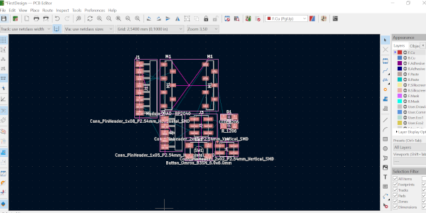
Now it was time to go to the physical side of things and to PCB editor! In schematic, I pressed open PCB in board editor from the top panel. It opened up the editor, and all our parts were in a nice, mixed bunch.
Before starting to detangle, I made a 5x5 cm rectangle in Edge cuts. This way it would be easier to start the fitting in. I also made the corners round by choosing the lines, right-clicking the mouse and choosing to add a fillet (value of 5). <(p>)
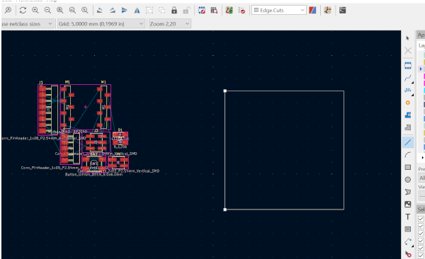
The placing went on accordingly to the schematic. Some parts were flipped, rotated etc. The 8- and 5-pin headers needed to be in a certain way close but not over the border so that they wouldn't crack easily when in use.
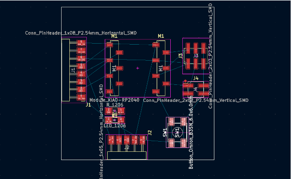
Now I needed to start making the connections that the lines showed me by using Route Tracks tool on the right tool panel. Track was set to 0.4 mm. Then it was just with trial and error to try to get the connections right and fitting everything in without overlapping.
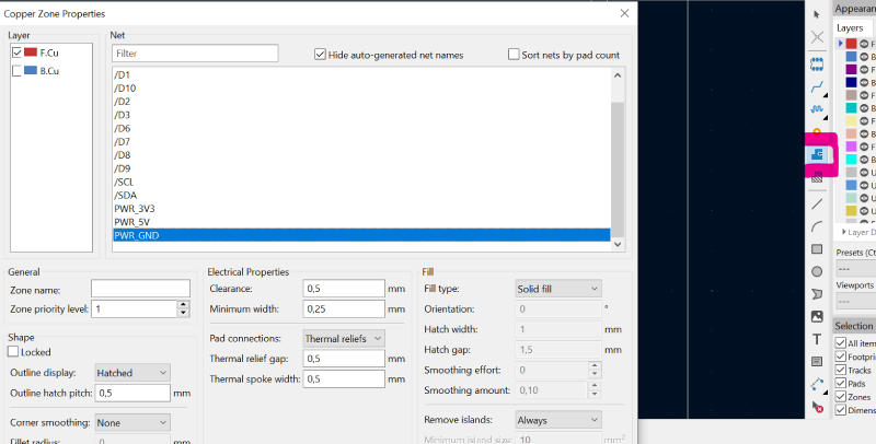
When everything was connected except for the grounds, I went on to set up a fill that connected the grounds to the filled area of the PCB. In Copper zone properties the layer F.Cu was chosen, and I set Clearance and Minimun width to 0.4 mm. From the right I chose PWR_GND. Then I pressed Add a filled zone in the tool box.
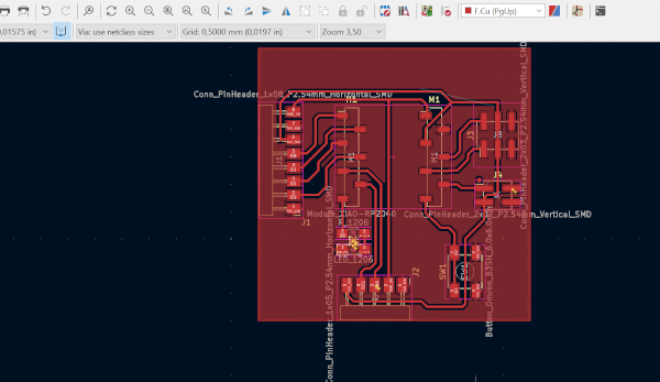
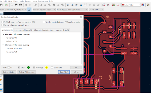
Now in design rules checker it showed first of all, some connections that didn't have en end-point to them, and more importantly it showed that some of the ground were not connecred. The first problem was easy to fix, as there just happened to be some small points of route I had added on top of the parts and didn't see them at first. When I deleted those, the warnings went away.
But the ground thing was more hard to fix. I noticed that in the editor it showed a few tiny lines that were crossing some route here or there, and those were the places the connection was not abled (for example in upper right corner in previous photo.). I looked around and understood that the only thing to do was to make some routes again in a different way. I tried some options, but some times ended up with more problems. But then finally, I got it right by moving the route starting from pin 6 in the 8-pin connector. Now when I run the design rules checker, the problems were gone. Victory!
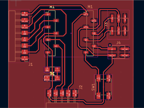
I made the holes to the corners with Draw a circle. In the end I also did some finishing work to some of the routes, for example removing sharp turns etc. That was it! Here is the finished board.
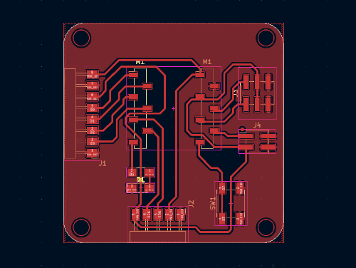
It is ready to go to the electronics production week. Well, at least I hope so. This was very interesting and fun experiment, and I'm sure it will be even more fun when I learn more about electronics bit by bit. KiCad seems to be a rational and clear program, and I enjoyed using it. Also it didn't slow down or crash at any point, so that's quite nice.