6. Electronics design
Group assignment for this week:
- Use the test equipment in your lab to observe the operation of a microcontroller circuit board
The documentation of group assignment can be found on our group work page.
In this week's group work we used a multimeter to measure current of Seeed XIAO RP2040 microcontroller. These measurements have been interesting because I am not good at using a multimeter or an oscilloscope. The results of the microcontroller current measurements were low. We tested different LED blinking codes and also the ring oscillator test code. In all of these, the results came out to something between about 25-37 mA. We got the highest value when we blinked different colors with the RGB LED, we just didn't notice to capture the color. However, there were no big differences in current between any of these tasks.
Individual assignment for this week:
- Design a development board to interact and communicate with an embedded microcontroller
Design a development board
In this week's local lesson we were introduced to the KiCad electronics design program. We practiced using the KiCad and made our first development board design.
First step was to download and install KiCad. We were given link to download the Fab electronics component library from gitlab to our computer. We also got a folder "own_library.pretty" from our instuctor. The folder included a kicad mod file for XIAO socket. Next, I added them to KiCad:
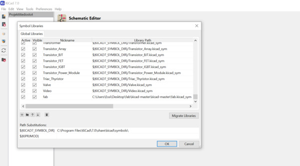
Go to Preferences -> Manage Symbol Libraries -> add fab.kicad.sym:
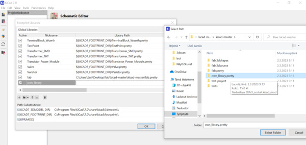
Go to Preferences -> Manage Footprint Libraries -> add fab.pretty and own_library.pretty:
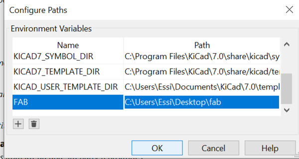
Go to Preferences -> Configure Paths -> add path for fab that points to the installation directory of the fab library:
Schematic Editor
Our insctructor had an example development board and our task was to design the same kind of development board. Our instructor showed us the process step by step.
I created a new project from File -> New Project and named and saved it. When editing schematics and board files, KiCad automatically saves the work periodically. You can change the time of automatic saving in the preferences. First step was to open schematic editor and make a schematic drawing of development board.
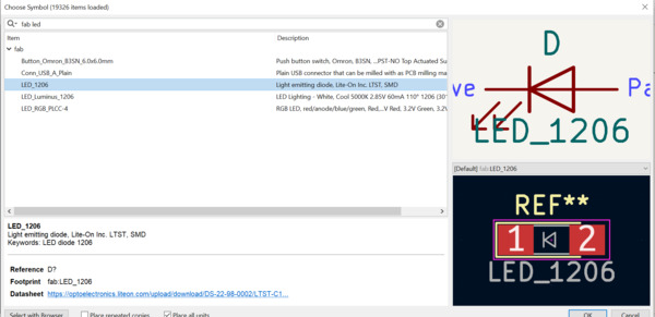
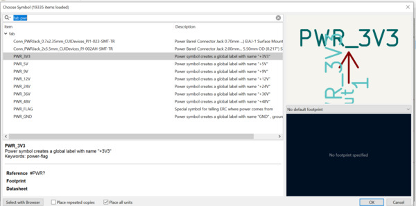
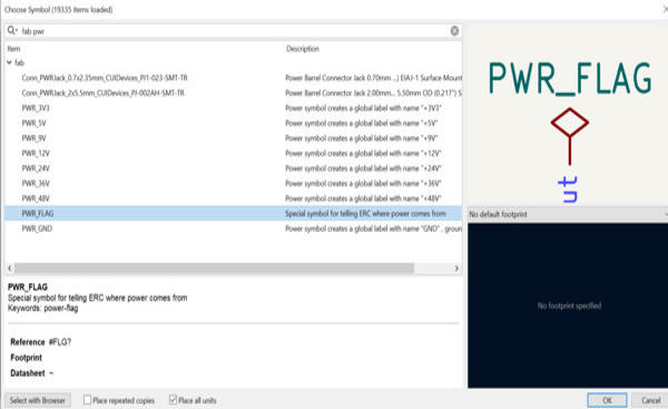
I added the parts of example board by using "Add symbol" tool found on the top right of the page. When I clicked on the drawing area, a new window opened and there I could choose a symbol. We used the fab symbols so I wrote fab first each time I was looking for a specific symbol. In the pictures below, I searched for the symbol for the right LED (LED_1206) and the correct power symbols.
|
|
Overall, the following symbols were added to the schematic: the module XIAO RP2040, LED 1206, resistor 1206, 6 x 6 mm button, 8-pin male connector, 5-pin male connector, connector header Surface Mount 4, connector header Surface Mount 6 and the correct amount of 3V3, 5V and ground power symbols.
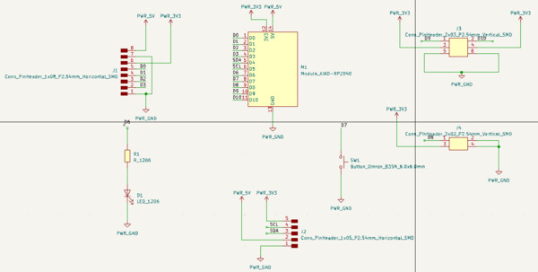
Next, I started to connect the right power symbols in the right places according to the model given by the instructor. I activated the connecting wire tool by clicking on the "Add a wire" tool in the toolbar on the right. Then I just clicked on the right symbols. I then added the labels to all the rest of the pins. First I made a short wire to which I could add a label. The tool for making labels can be found in the toolbar as "Add a net label". Picture below left.
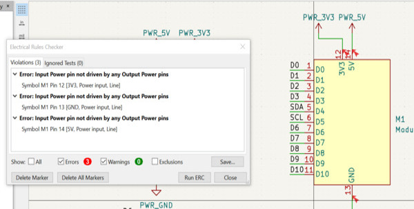
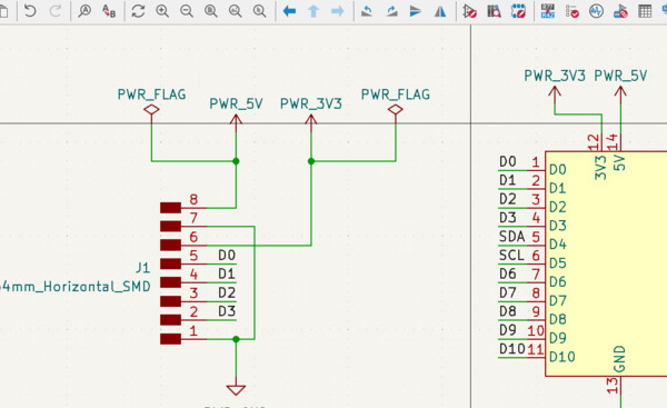
I checked the schematic using the "Perform electrical rules check" button in the top toolbar. When I pressed the "Run ERC" button, the program gave me a few errors "Error: Input Power pin not driven by any Output Power pins". Picture below right.
|
|
These errors were fixed by adding PWR_FLAG symbols where needed. Pictures below.
|
|
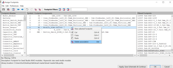
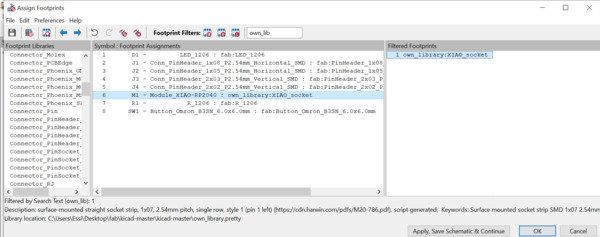
In the Shematic editor, the last step was to check the footprint assignment. To do this, in the top toolbar there is a button "Run footprint assignment tool". Here we changed the Module XIAO-RP2040 association. First, the previous association was removed. Picture below left. Then we searched for a new association own_library:XIAO_socket, which we got from our instructor at the beginning of the lesson. Picture below right.
|
|
Now that the schematic is complete, I pressed the "Open PCB in board editor" button on the top toolbar and next started editing the board there.
PCB Editor
In PCB Editor I first pressed the "Update PCB with changes made to schematic" button and got the components in the area.
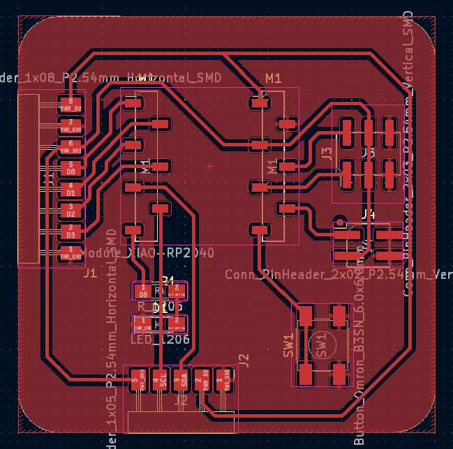
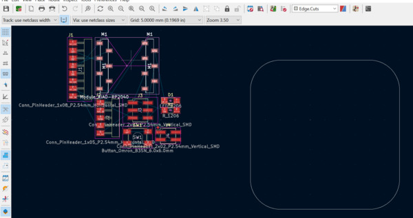
Before I started to place the components in order, I drew a board of about 50 x 50 mm. I changed the grid to 5mm, which made it easier to draw, and then selected the Edge Cuts layer from the top menu, where I could draw the outer edges of the board. Then I just clicked on the square of the right size for the area. I rounded the edges by drawing a circle inside the corner and removing the extra lines. Picture below. Petra had found an easier way to round the corners:
- select the lines connected to the corner
- right click
- select Fillet Lines
- fill-in a number
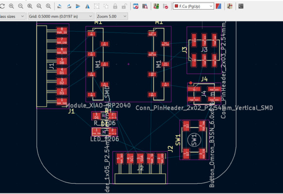
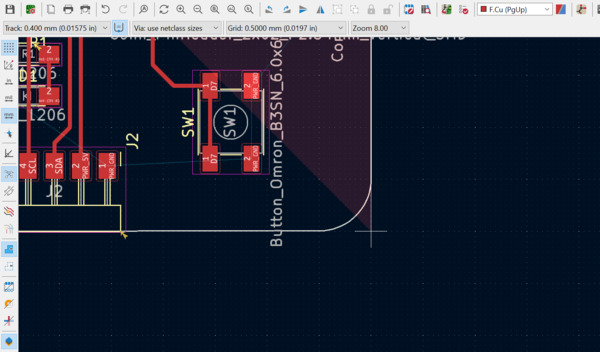
Next, I placed the components inside the square in pretty much the same places as we had planned in the schematic. Some of the components had to be rotated or flipped the other way around to get them right on the board. I changed the grid back to a smaller 0.5 mm at this point to make it easier to place the components. Picture below.
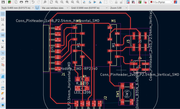
I changed the layer back to F.Cu and started drawing tracks. First I set the track width to 0.4 mm in the track menu in the top left corner. Then I selected the "Route tracks" tool from the right toolbar. The blue/green thin lines connected the pins and helped to draw the tracks. This was a surprisingly fun step to try to figure out how the tracks would go. Picture below.
Especially when making tracks in tight spots, it was easier to select the shove option in the settings, so that the tracks already drawn "gave way" to the new track. The setting can be found in the Route menu -> Interactive Router Settings.
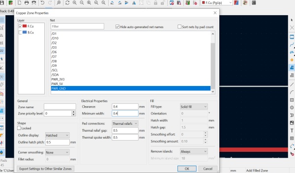
Once all the other tracks were drawn except the ground, the ground was connected by filling in the area. I selected the "Add a filled zone" tool from the toolbar on the right and clicked on one corner of the board. The Copper Zone Properties window opened, and I selected F.Cu as the layer, set the Clearance and Minimum width to 0.4 mm, and from the Net menu, I selected PWR_GND to connect the ground. Picture below left.
I then drew the area by clicking on each corner of the square. Picture below right. I was able to make the fill visible or hidden by pressing the "Show filled areas of zones" button on the left toolbar.
|
|
Finally, I pressed the "Show the design rules checker window" button at the top and then the "Run DRC" button. The only warnings were "Silkscreen clipped by board edge", which didn't affect our design, so the first design for the development board was done! Below is a picture of the finished board design.