Week 6
Mar 01: electronics design
List of task this week
Group assignment
To see the group assignment go here.
My thoughts on this week’s group assignment use the test equipment in your lab to observe the operation a microcontroller circuit board: I have used a multimeter before, mostly to check connections but never a oscilloscope so this was a good lesson for me.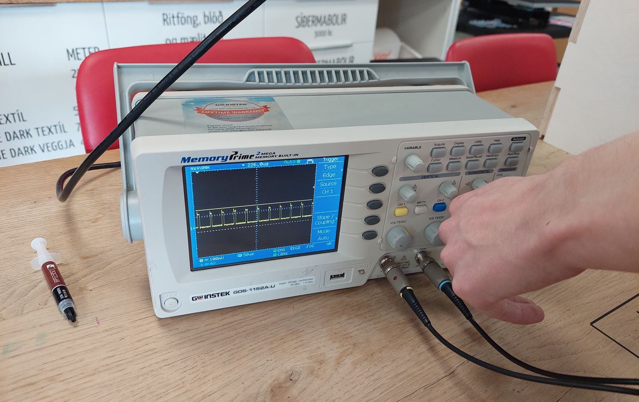
Design a development board to interact and communicate with an embedded microcontroller
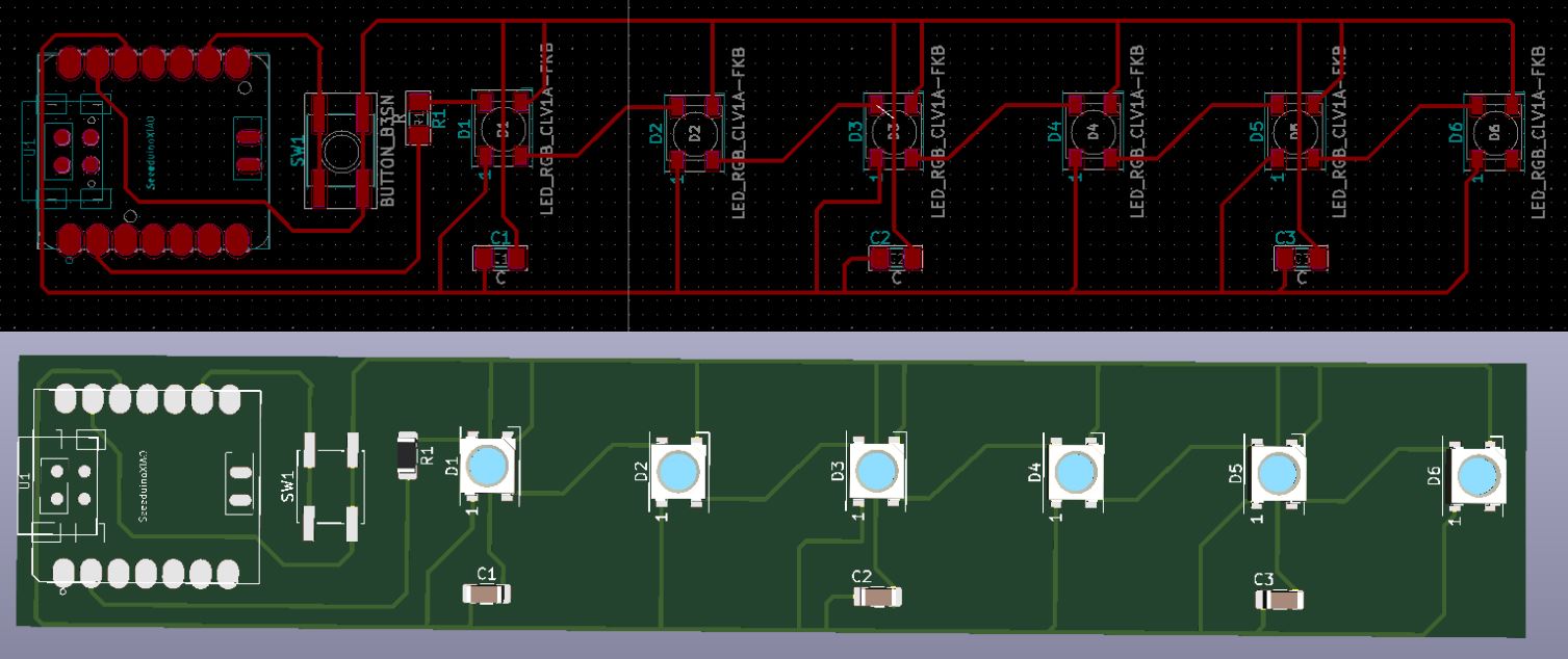
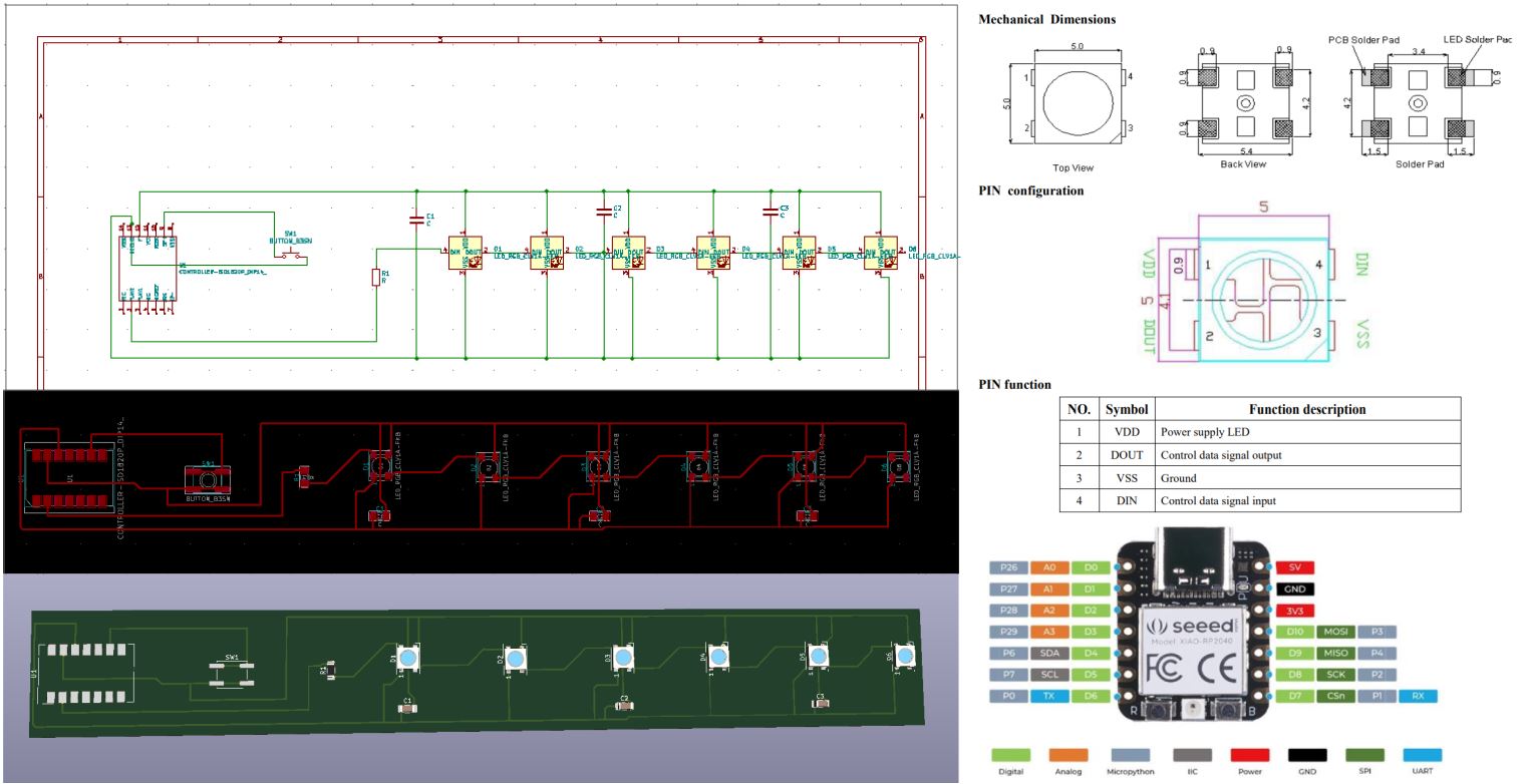
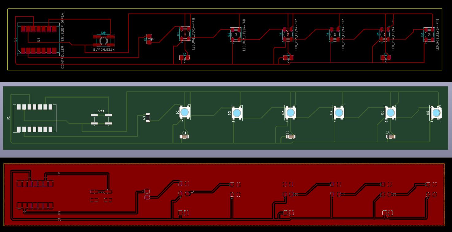
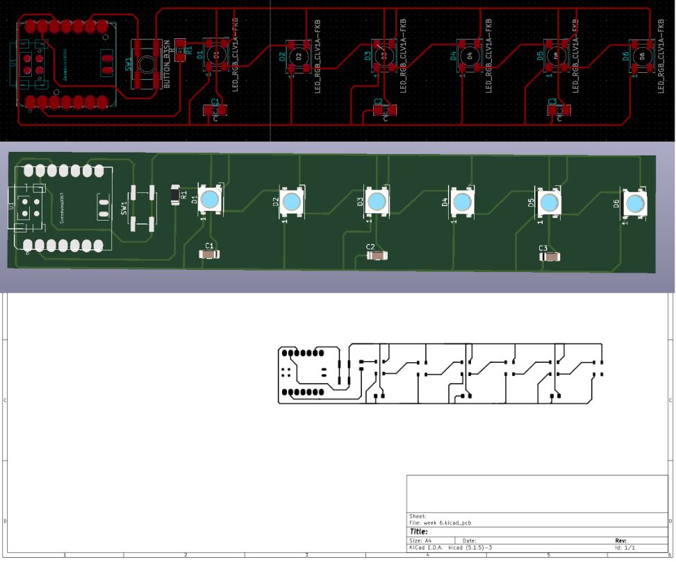
I want to make a pcb with 6 leds and a button so I can practice making different programs for my final project and I want
there to be as much space between the lights as I can get away with. Since I have only used Kicad once before and that was in 2019 I started with a
youtube tutorial to learn the basics to help me make my
circuit later. It of curse wasn’t a circuit just like the one I was going to make but it did go through all the steps so
I a lot from it but a lot also came later through trial and error.
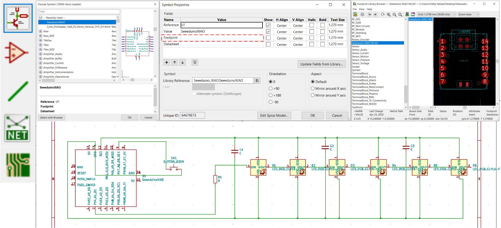
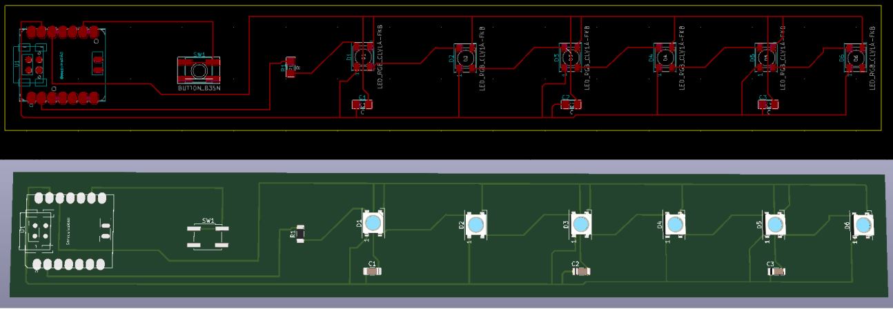
Turns out I was connecting the compositor wrong so I got some tips from my work college Arnar and fixed that. Also turns out that in the tutorial I watched first they make the whole board ground, and I don’t want that so I went back a little.
The next day I was talking to my other college and fellow student and he had found the XIAO rp2040 footprint for Kicad and sent it to me so I went back and fixed that. So to talk about how I did it the right way, I opened Kicad went to file and selected new project. Once I saved it in place and went into Schematic layout editor. There I selected Place symbol, clicked somewhere on the screen and selected the component I was going to use in my project. Make sure it has a footprint by clicking it and seeing if there is something in the footprint spot, if not click it to find one. Once I had all my components with the footprints I used the tool Place wire to make the connections of the project. To save those changes I clicked Generate netlist, clicked the Generate netlist button and saved.
That done I went to Run Pcbnew to layout printed circuit board. There I moved the components into place and connected them with route tracks. Once I was happy with how that looked, I went to File-Export-SVG.
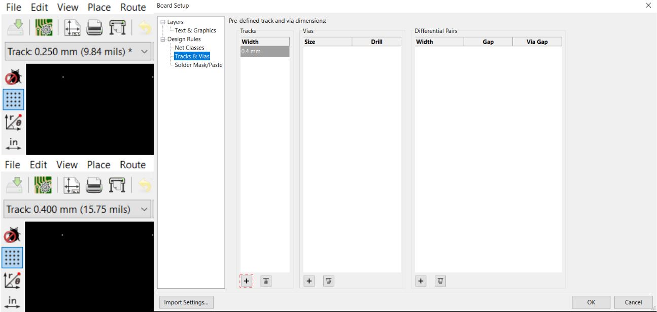
When I thought I was all done I realized that our coper plates are only 15cm so I had to put all the components closer together. To do that I deleted the traces selected the components one at a time pressed M and moved them closer together. Before I made new traces I made them thicker, to do that I clicked track and selected Edit predefined sizes…, clicked the + at the bottom of the tracks column and wrote 0.4mm, and clicked OK.
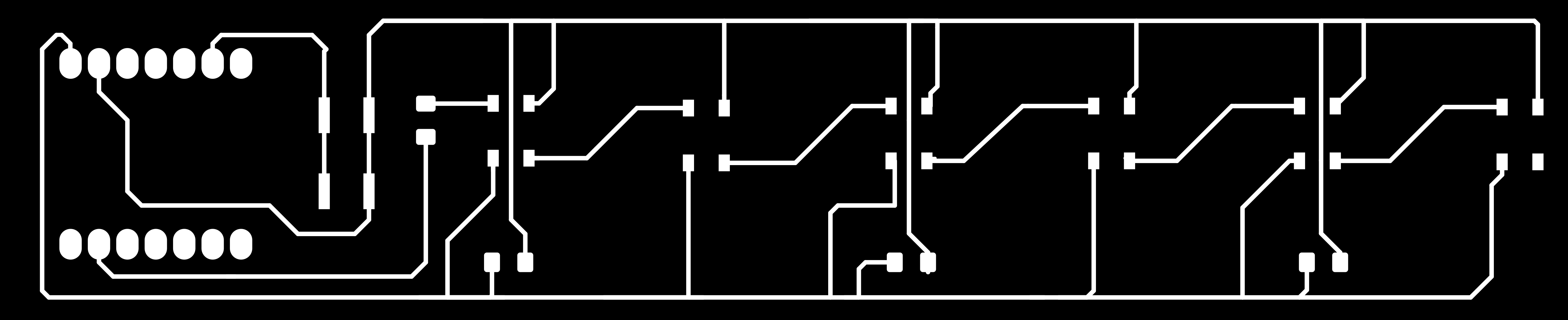
After that I exported the pcb as SVG and will use that to make PNG files to mill out in two weeks.