6. Electronics design

For this week, as an individual assignement, a development board that interact and communicate with an embedded microcontroller should be designed
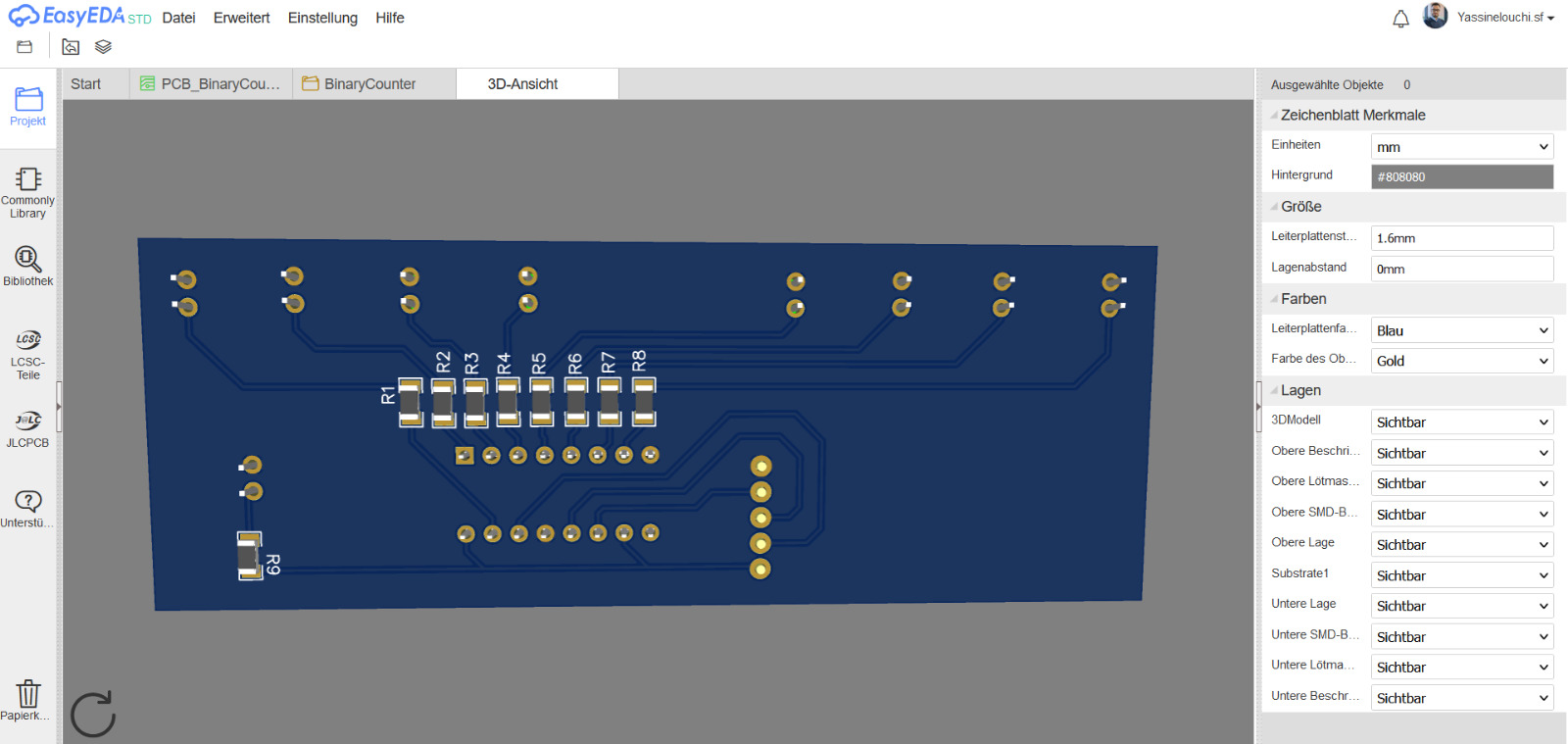
EasyEDA

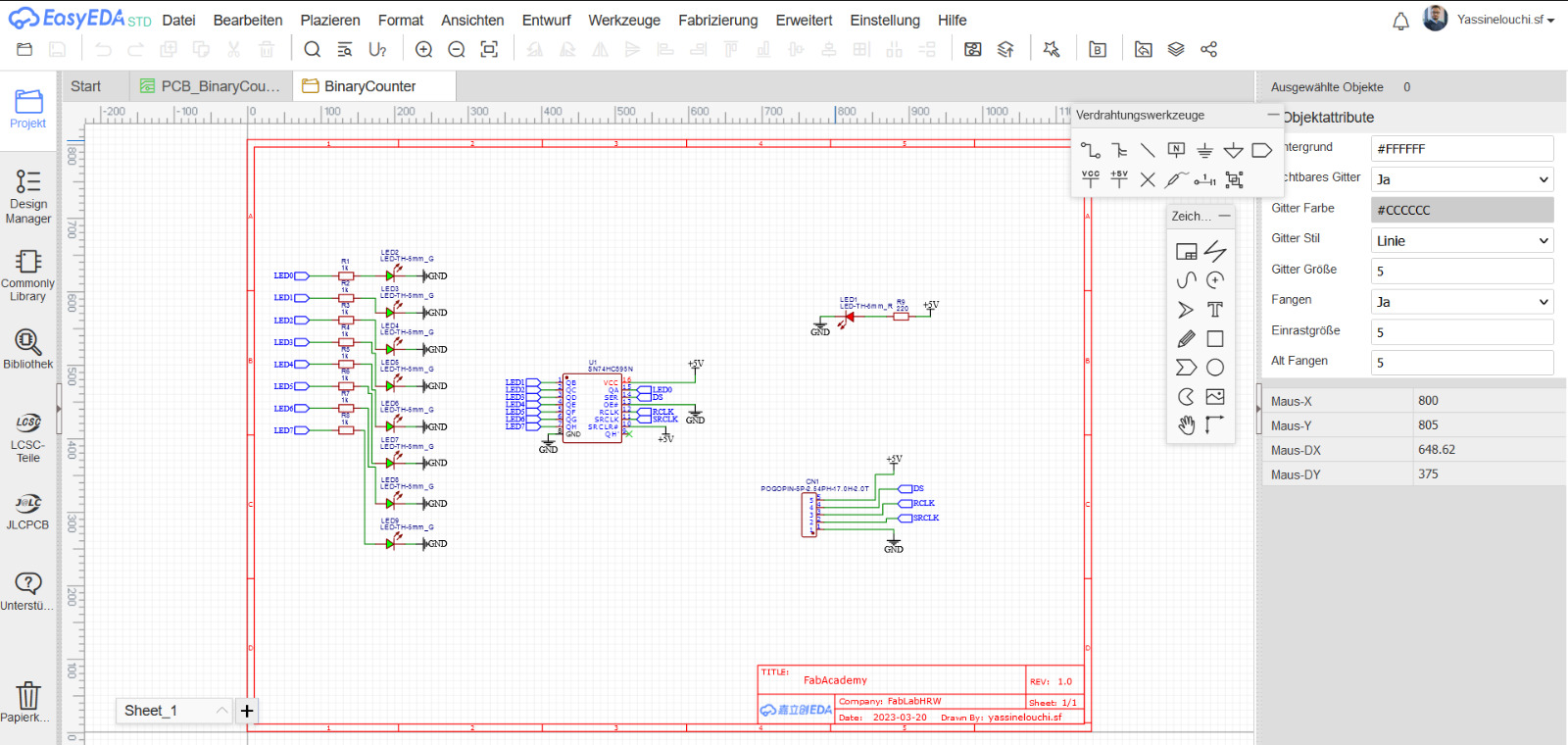
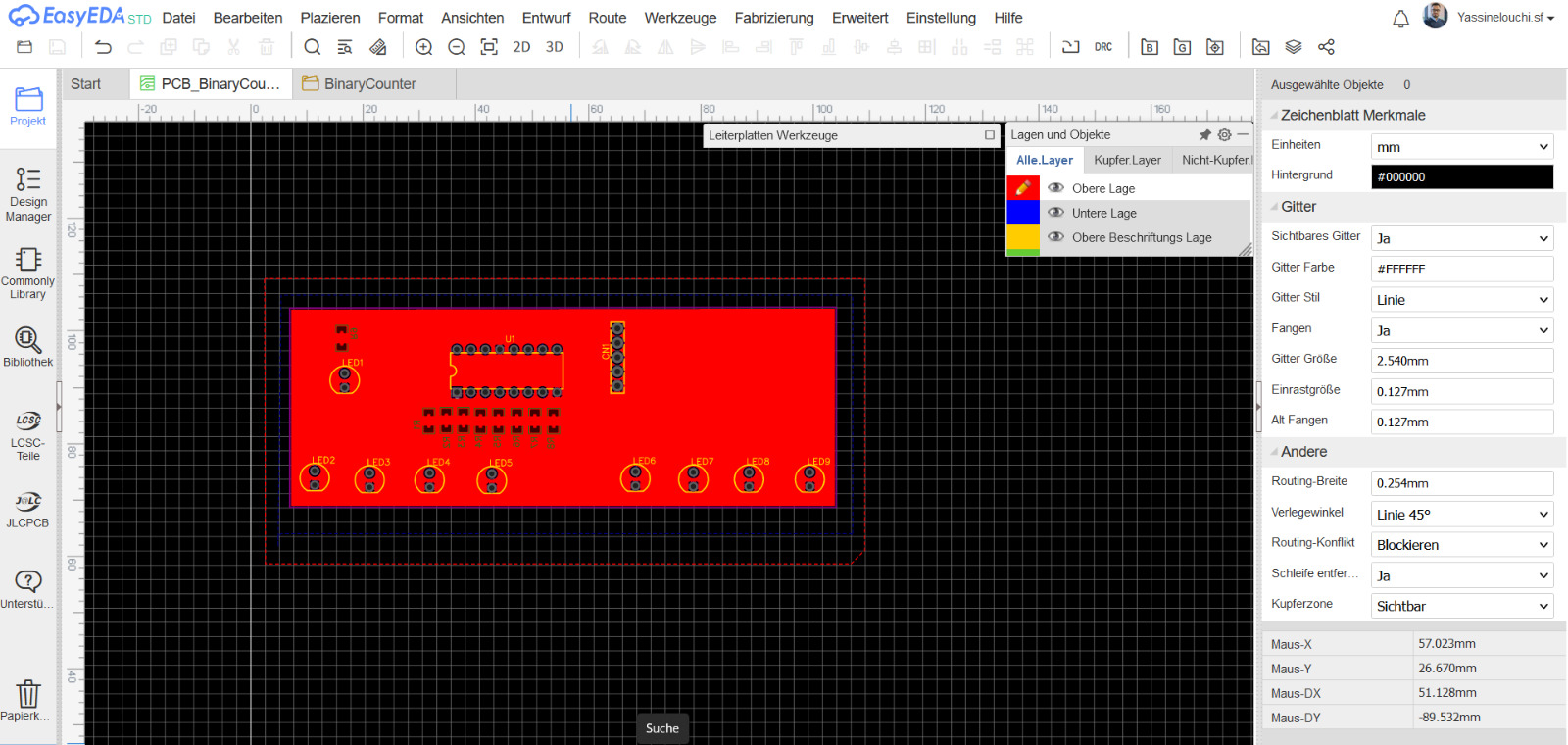
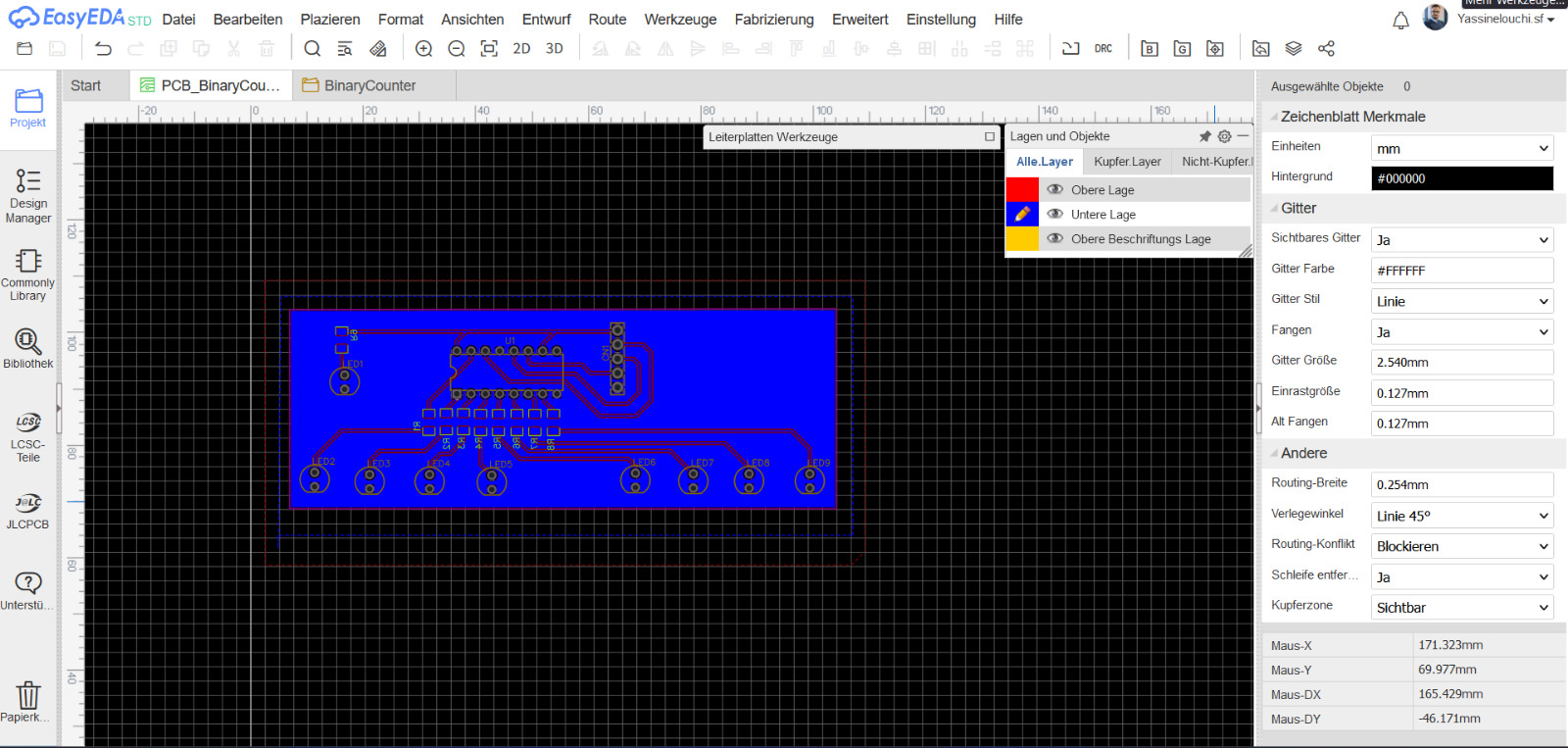
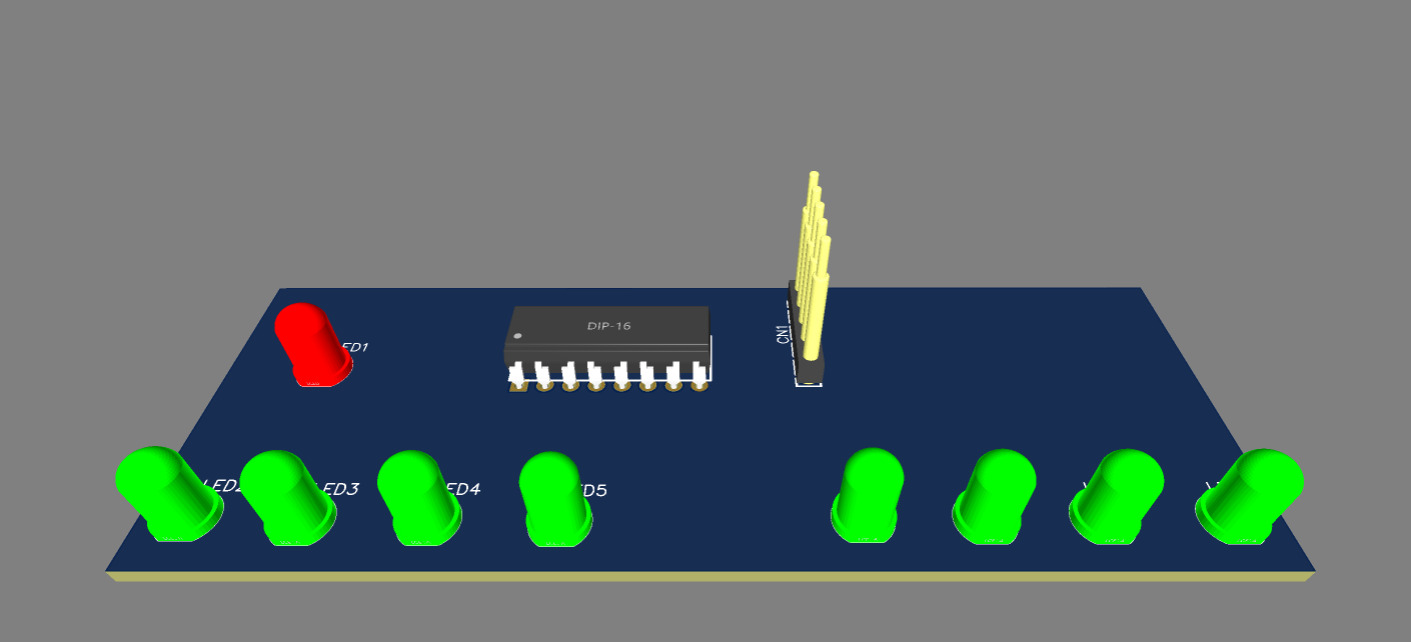
EasyEDA is a free, web-based Electronic Design Automation (EDA) software that allows users to create schematic diagrams, printed circuit board (PCB) layouts, and simulations for electronic projects. It provides a user-friendly interface and a wide range of components and modules that users can use to design and test their electronic circuits.

With EasyEDA, users can design their circuits by dragging and dropping components onto a canvas, and then connecting them together with wires. They can also simulate the circuits to test their functionality and performance, and generate a PCB layout for their circuit design.

EasyEDA also provides a large library of components that users can use in their circuit designs, including microcontrollers, sensors, power supplies, and more. It also has a collaboration feature that allows multiple users to work on the same project simultaneously.

Overall, EasyEDA is a great tool for hobbyists and professionals alike who want to design and test electronic circuits quickly and easily.

Electronic design in EasyEDA

To design a PCB using EasyEDA, a web-based software tool, the following steps can be followed:

  1. A new project can be created on EasyEDA with a relevant name and description.
  2. Components can be added to the circuit design and connected with wires using the schematic editor. Annotations such as values and labels can also be added.
  3. The built-in library can be used to search for and add components to the schematic.
  4. PCB
  5. A netlist file can be generated that describes the electrical connections between components in the circuit.
  6. The netlist file can be imported to the PCB editor to create a PCB layout based on the schematic design.
  7. The components can be placed on the PCB, traces can be defined, and power and ground planes can be added.
  8. The PCB library can be used to search for and add footprints for components.
  9. PCB PCB
  10. A design rule check (DRC) can be run to ensure that the layout meets the design requirements and manufacturer's guidelines.
  11. Gerber files can be generated, which will be used by the manufacturer to create the physical board. Drill files can also be generated if the board requires drilled holes.
  12. The design can be previewed to ensure it meets the intended requirements.
  13. The board can be ordered from a manufacturer or the design files can be exported to manufacture the board.

Additional features such as simulation, BOM generation, and 3D view are offered by EasyEDA for designing and analyzing circuits.

PCB PCB

Check out our group assignment: Group Assignment