8. Electronics Design
Reflection
In this electronic design, I remember in 2022 that I referenced Andrian's model but his design had 0 Ohm resistor so I redid it.
Then I redesign for ATTINY 1614, ATTINY85, ESP32 Xiao C3 boards in both EasyEDA and Fusion360 over the 2 years. It was an interesting experience though I would say I am still not strong like leadaing industry experts but I am sufficient for my original intent to be able to read basic schematics, to design basic and improve basic. Also tried some udemy courses like.

Many Thanks to Steven for teaching how to design my final project PCB to avoid using too many 0 ohm resistors.
Group Assignment
- Use the test equipment in your lab to observe the operation of a microcontroller (MCU) circuit board (as a minimum, you should demonstrate the use of a multimeter and oscilloscope)
Attached is the link to group assignment
Individual Assignment
Checklist for this week:
- ☑ Linked to the group assignment page: For group assignment I am suppose to send to board house, in step 9 is my process to send to board house.
- ☑ Documented how you made (mill, stuff, solder) the board
- ☑ Documented that your board is functional
- ☑ Explained any problems and how you fixed them
- ☑ Uploaded your source code: here is my file for blink for more codes for this pcb refer to output, communication and input topics. here is file for the EasyEDA Json file zip
- ☑ Included a 'hero shot' of your board
Workflow for Circuit Design in EasyEDA
The process of designing a printed circuit board.
| Step | Description | Key Actions and Considerations |
|---|---|---|
1. Project Creation 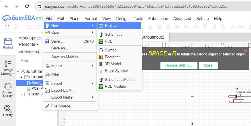
|
I create new project in EDA for my design files. | Create a new project folder within EDA's control panel to keep schematic and board layout files together. |
2. Schematic Design 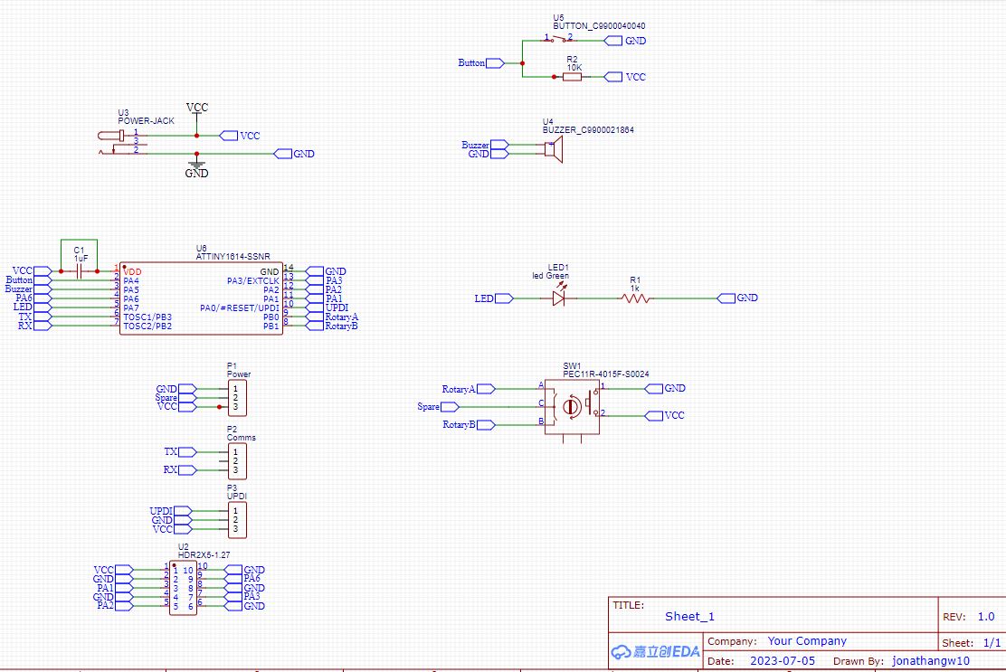 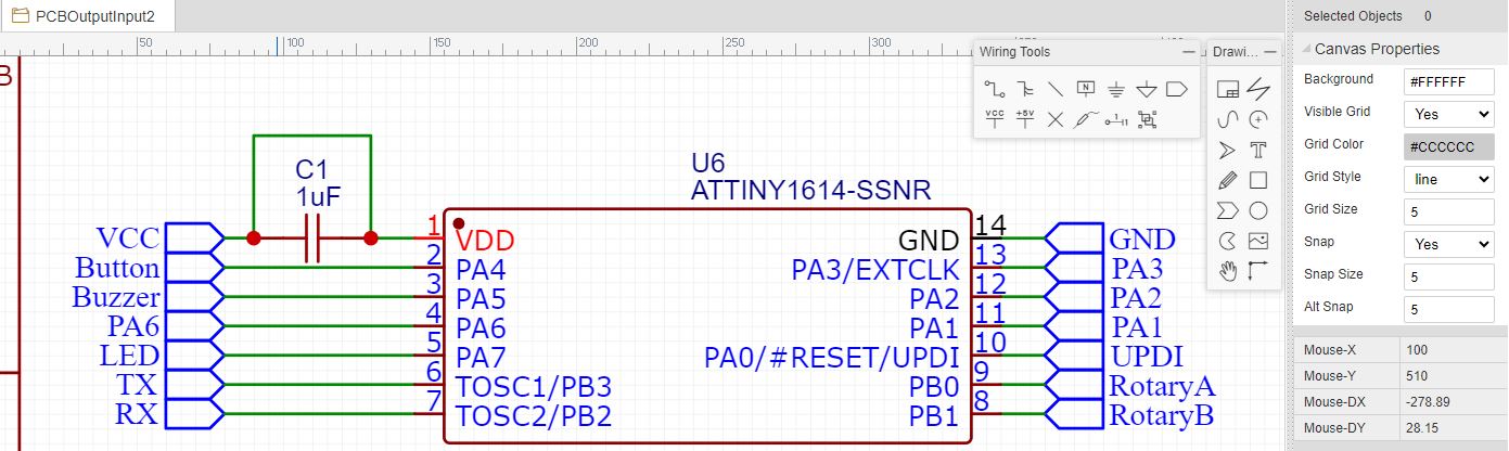 |
I start with the circuit schematic, which is a symbolic representation of my circuit. Next I am going to search and drag the components needed. | Use the Schematic Editor to place and connect component symbols. Ensure all components are correctly connected according to my circuit design. |
3. Component Selection 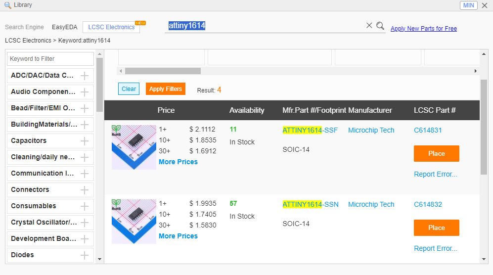 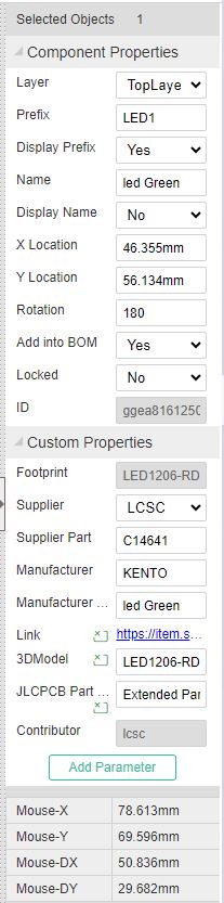 |
I Choose the physical components for design from EAD's libraries. | Select components based on their electrical characteristics and physical footprint. Use the Library Manager to find or add new components as needed. |
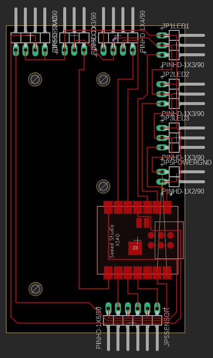
4. Board Layout 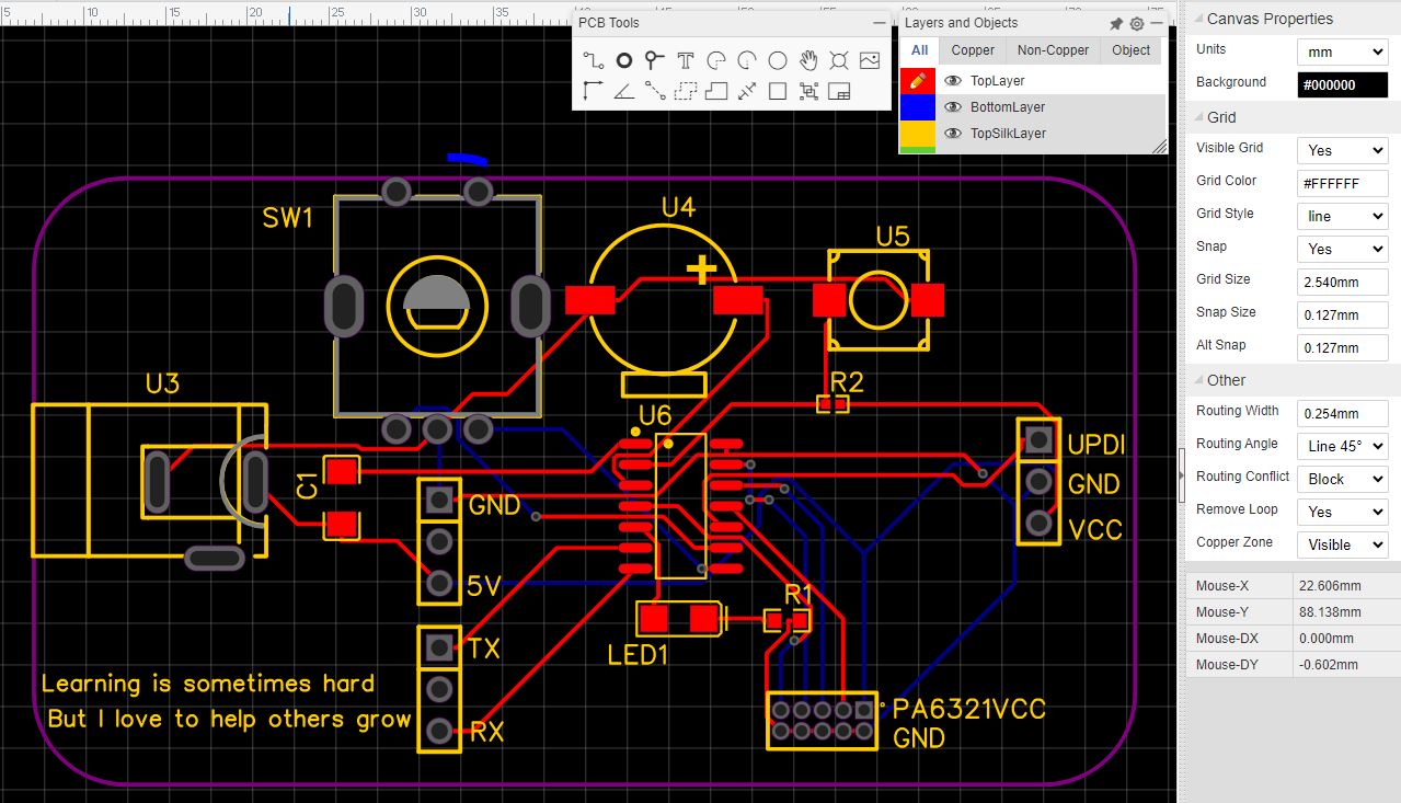 |
I swtich from schematic to physical board layout. Then I slowly put all the items onto the layout and route using the method taught. | Switch to the Board Editor, where EDA automatically creates a board from your schematic. |
5. Design Rule Check (DRC) 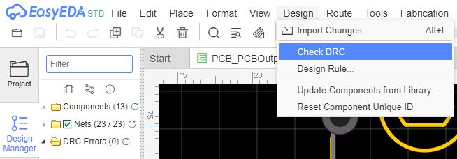 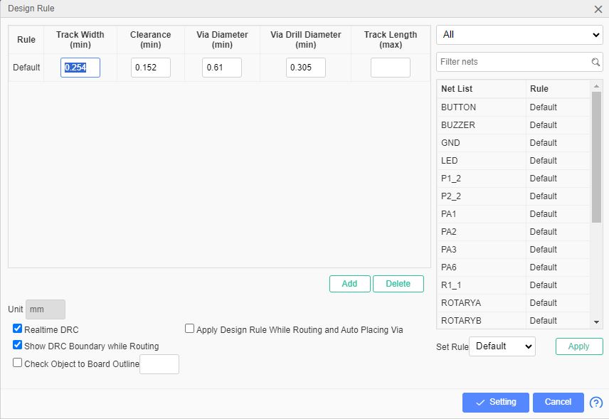 |
I Ensure went to iput the Design rule chcek settngs. | Run the DRC tool to check for errors like trace spacing, pad overlaps, and unconnected signals. Adjust your design to fix any issues. |
6. Generating Gerber Files
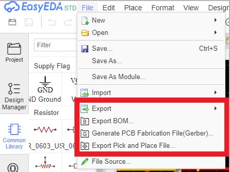 |
Using the Export Function, I geneerated the Gerber file. | Once design passes DRC and ERC, use the CAM processor to generate Gerber files, ie standard format for PCB fabrication. |
8. Bill of Materials (BOM) Creation
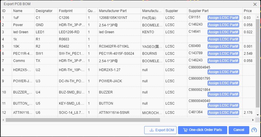 |
I liek EasyEda as it allows easy Compile a list of all components required for the PCB. | Generate a BOM from schematic, listing all components with their values, package types, and quantities for procurement. |
9. Setting SpecificationsOrdering (Board House ordering which is group project)
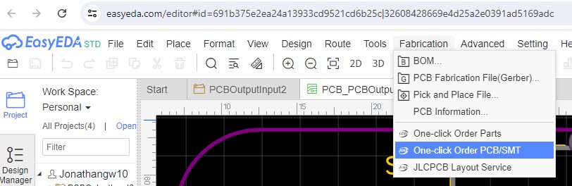 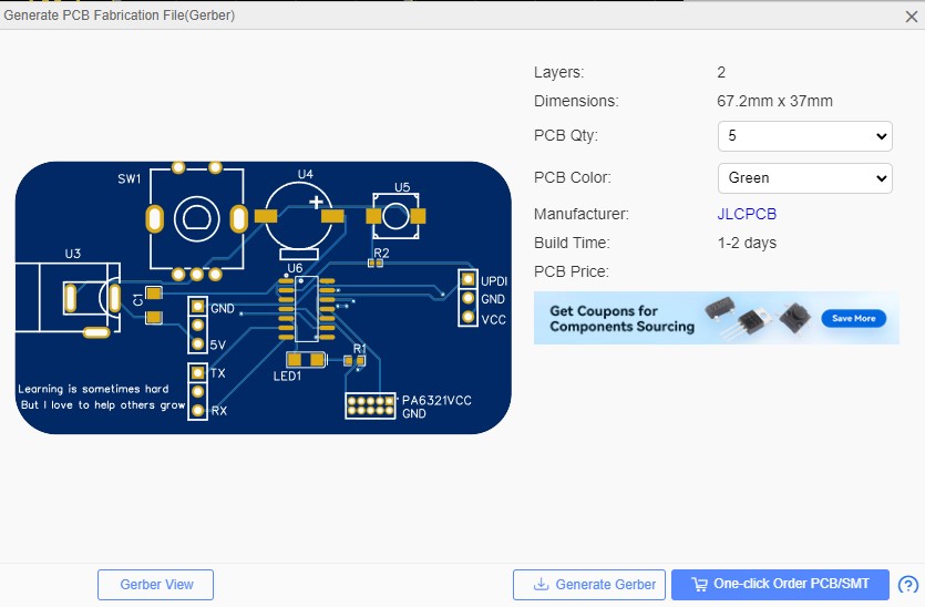 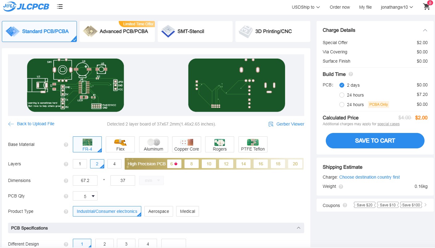 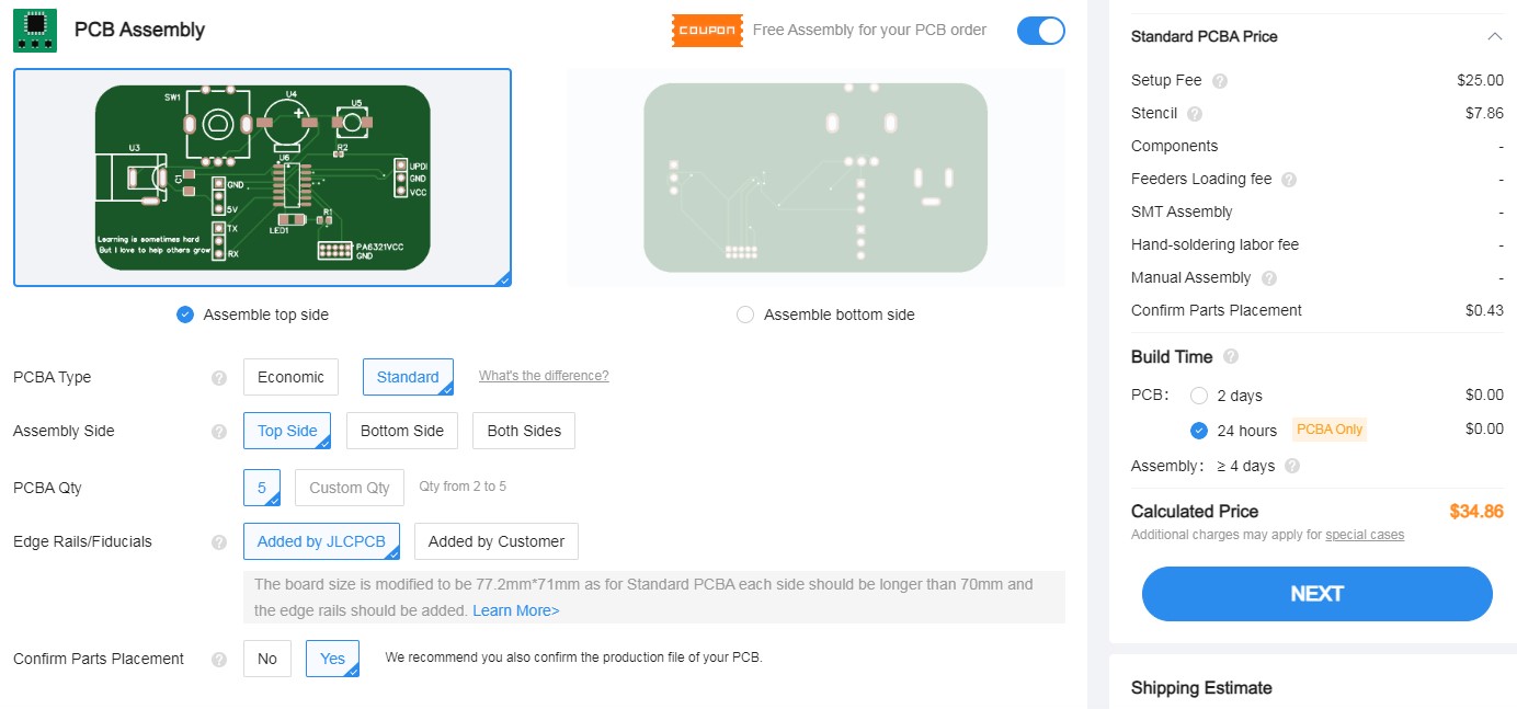 |
At EasyEda, i used the one click fabrication and selected specifications of PCB and clicked on PCB Assembly and made payment. | Generate a BOM from schematic, listing all components with their values, package types, and quantities for procurement. |
10. Testing PCB
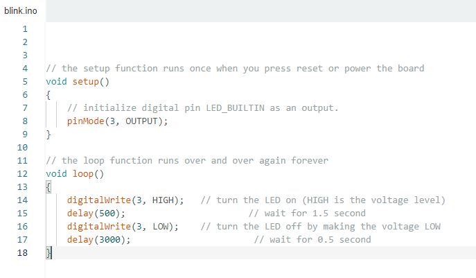 |
I manually tested continuity for each pin. I Create a blink sketch in the Arduino IDE tailored for the ATtiny1614. Pin 3 is being used. You can refer to output and input devices assignment to see other programming which i did with it. | Demonstrates the capability of the ATtiny1614 by executing codes. |
B2. PCB Components Detailed Overview
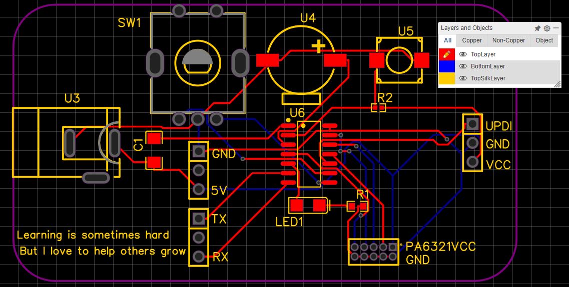
| Components I used | Technical Specification |
|---|---|
SW1 (Rotary Encoder) 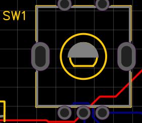 |
converts motion of shaft into electric signal |
U3 (DC Power Jack) 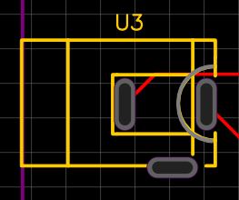 |
direct current (DC) power input. |
U4 (Piezoelectric Buzzer) 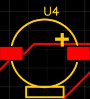 |
Component generate acoustic waves at a set frequency when an alternating electrical signal is applied across its piezoelectric material. |
U5 (Tactile Switch) 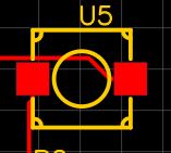 |
A momentary contact switch that can be tracked by input pins.. |
U6 (Microcontroller Unit) 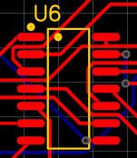 |
My attiny1614 that controls the input and output pin. |
R1, R2 (Resistors)  |
To limit current going to led. |
LED1 (Light Emitting Diode) 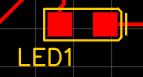 |
Light up when output pin of uC is activated. |
| 5V, GND, TX, RX (Power and Communication Lines) | (5V) and ground reference (GND), with transmission (TX) and reception (RX) lines for communication. |
| UPDI, GND, VCC (Programming and Power Interfaces) | UPDI interface for in-system programming and debugging of microcontroller units, ground (GND) and positive voltage supply (VCC) terminals . |
| PA6321 | PA pins: 6, 3, 2, 1 |
C1 (Electrolytic Capacitor) |
A polarized capacitor with a 10µF capacitance. |