4 - Electronics production
We learn the manufacturing process of a PCB from a design to the milling machine. To solder the board with SMD components and to program our circuits.
Summary
This week we start working with electronics. We learn to manufacture our PCBs and solder with SMD components.
Assigments
- group assignment:
- characterize the design rules for your in-house PCB production process
- extra credit: send a PCB out to a board house
- individual assignment:
- make an in-circuit programmer that includes a microcontroller:
- extra credit: customize the design
- mill and stuff the PCB
- test it to verify that it works
- extra credit: try other PCB processes
- make an in-circuit programmer that includes a microcontroller:
Group assignment
The link to Group Assignments of Fab Lab León is this
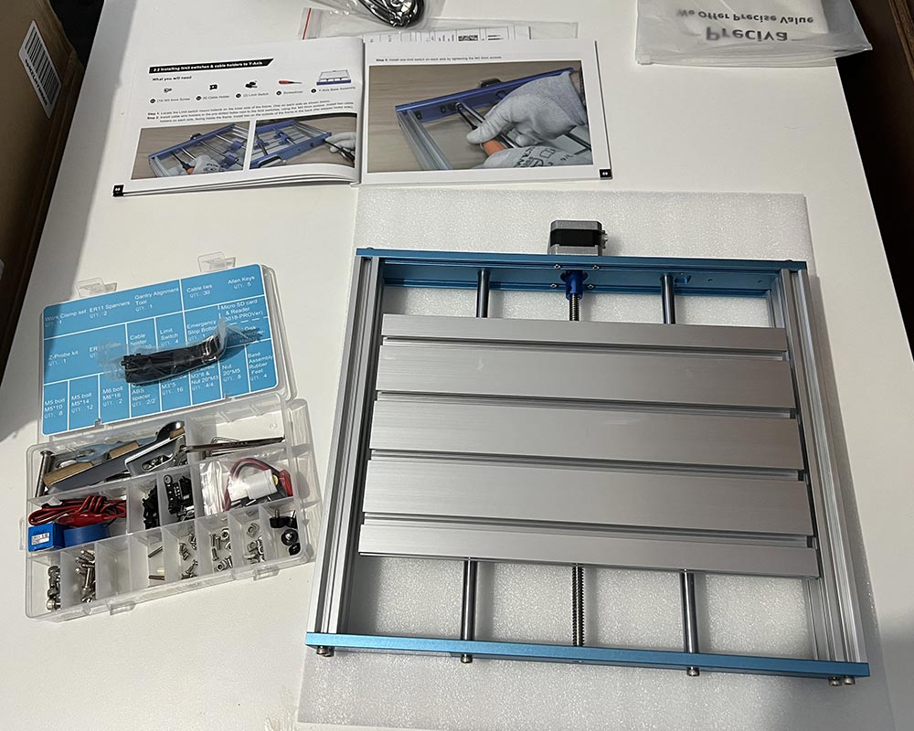
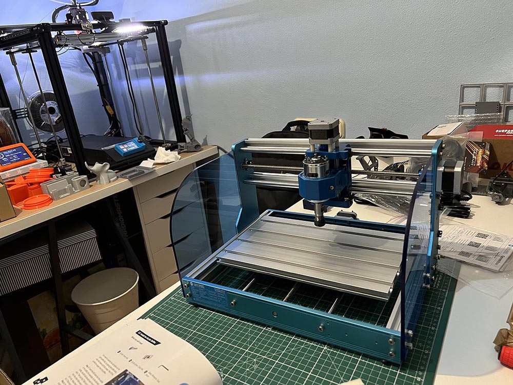
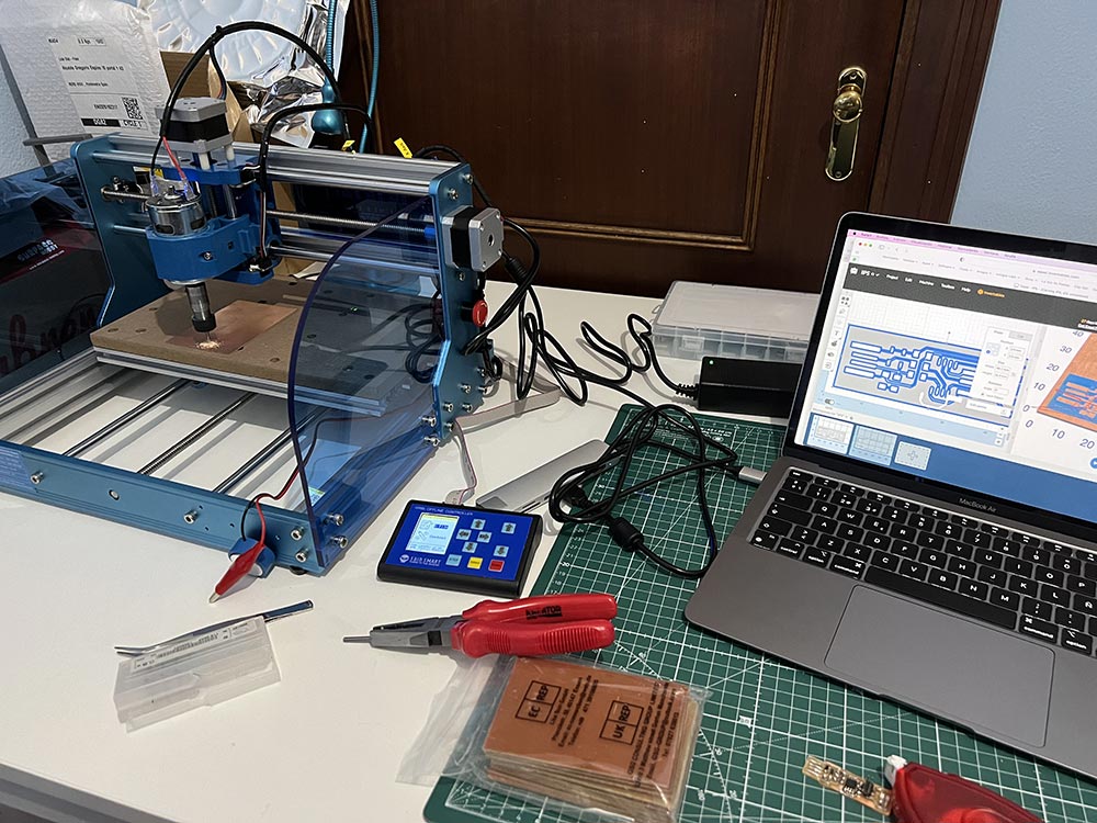
I will use the Genmitsu 3018-PRO (Resource Page)
The same Wednesday the 3018 arrived, before I started to assemble it I read the printed manual well, as well as the extensive online documentation that it has both on assembly and use.
My idea was to buy it before, but for a month there was no stock.
I was surprised how well packaged and documented it is, as well as all the details and accessories it comes with.
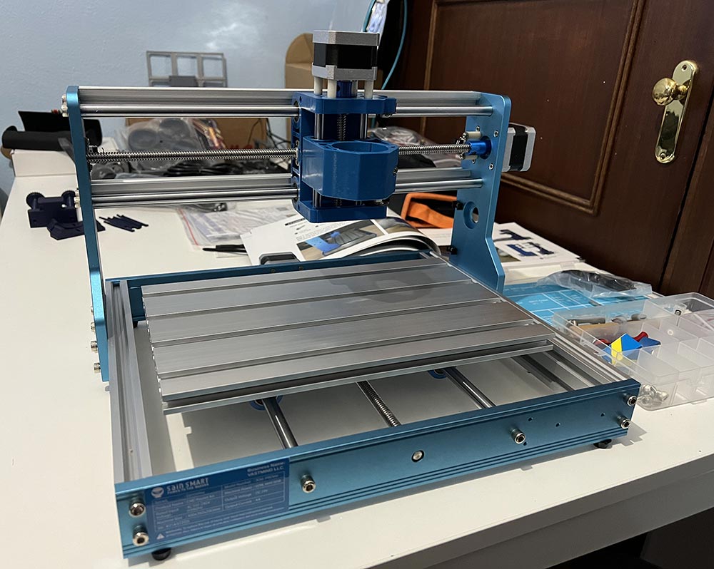
Build Millin machine
Parallel to the individual work I was assembling the milling machine.
Easel
After assembly I saw how to start milling. The manufacturer recommends for new versions of MacOS (Catalina, Big Sur, Monterrey….) to use Easel. Easel is a web-based software that allows you to design and carve seamlessly.
Only need install a driver in Mac, and work perfect in a MacBook Air M1.
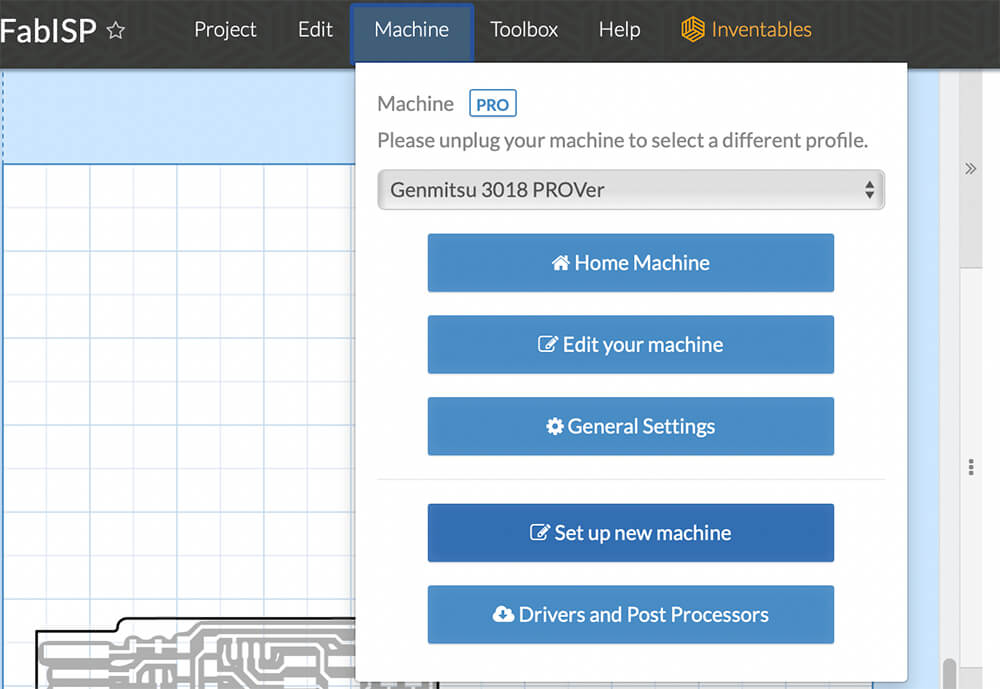
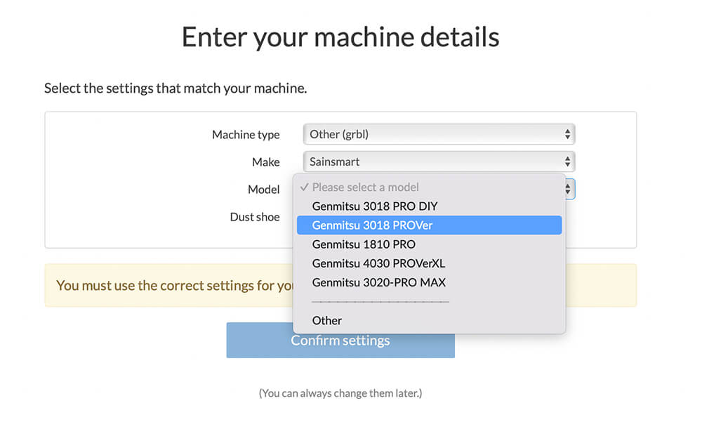
Setting the 3018ProVer
After register to Easel, the first is config your machine. From menu “Machine”, press “Set up new machine”.
Will open a list of Carve models or user Others (3rd party machines)
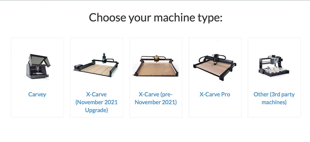
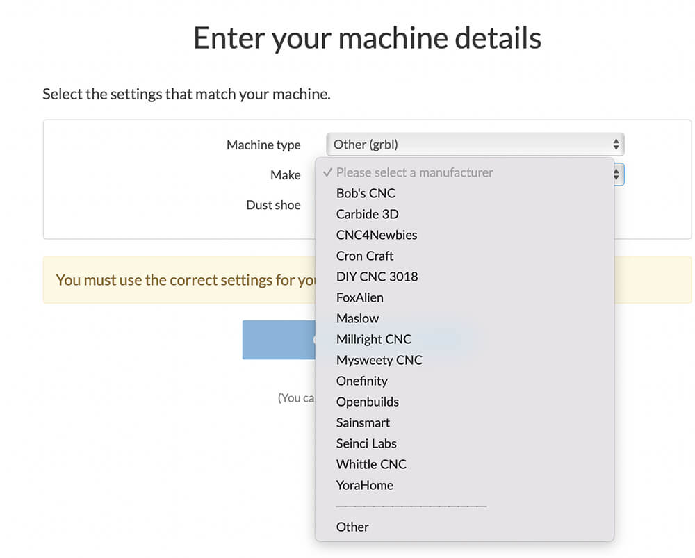
In my case i press Other and select my machine of a list, first the manufacturer “Sainsmart” and after the model “Genmitsu 3018 PROVer.
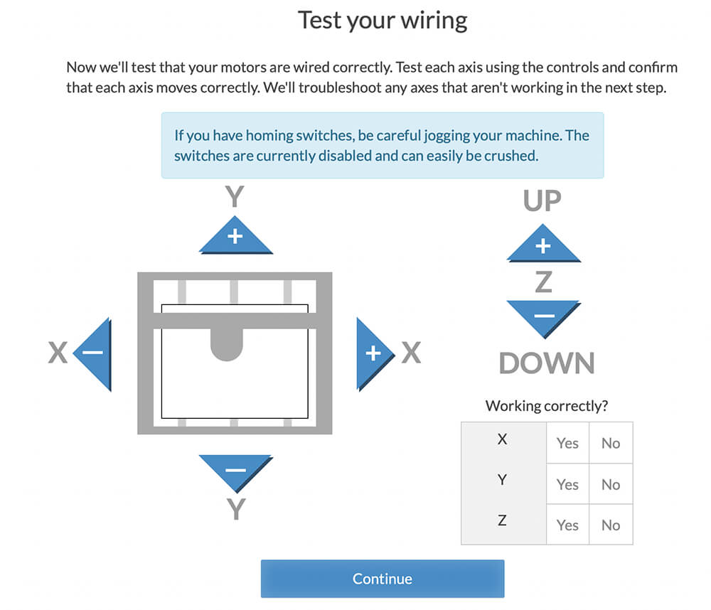
After this, the new window will ask for test the wiring, a small tool for move the XYZ axis, and if all work need press “YES” in the table.
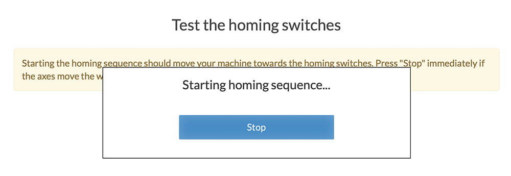
After press “Continue”, Easel made a test of the homing switches.
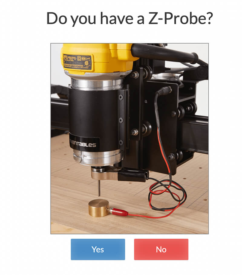
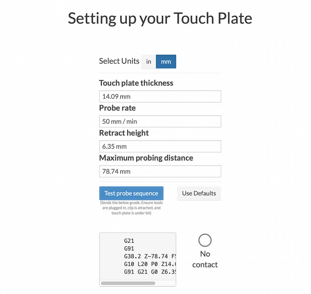
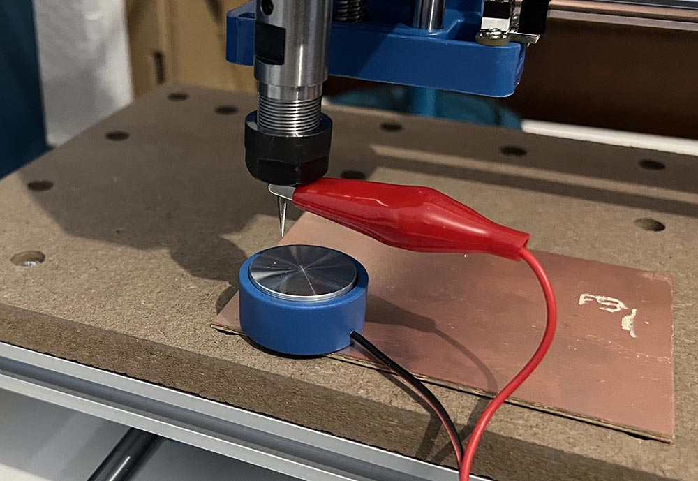
If you have a Z-Probe can set up in this point. And very importat edit advance setting.
Is very important configure good, in my case by default the touch plate thicknees is 14.09mm but Easel by default is 14.99mm, is very important set up good this, why the Bit will move 0.90mm down more when start to mill!
I edit too the probe rate, more slow and more precise.
And it´s all :)
Configure software
Easel can import SVG, G-Code, DXF or Image Trace, and have small tools for draw or made new designs.
I try import image, but is a bit hard, dont have controls for optimize the image, and the scale is not real to dpi, need edit or scale, and the vectorization it does is not very precise.
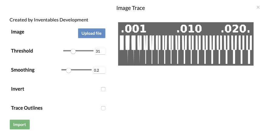
After this I open the PNG in Adobe Illustrator and vectorize, to export in .svg. I import the SVG file in Easel and the result was much better. Only i need delete leftover lines and objects.
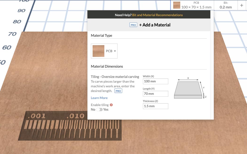
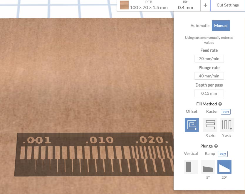
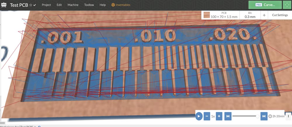
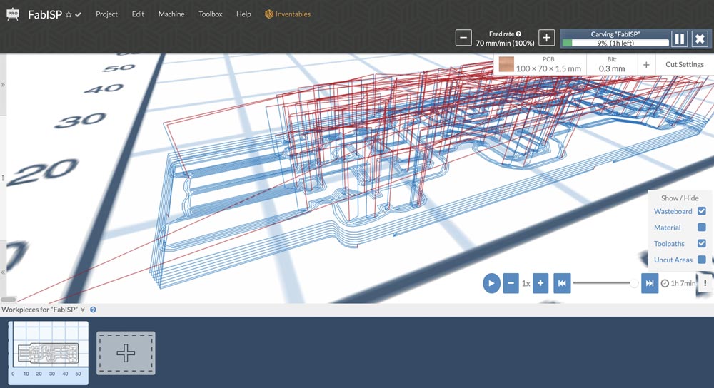
In right window i can set the type of surface to be milled. I will use PCB 100x70x1.5mm.
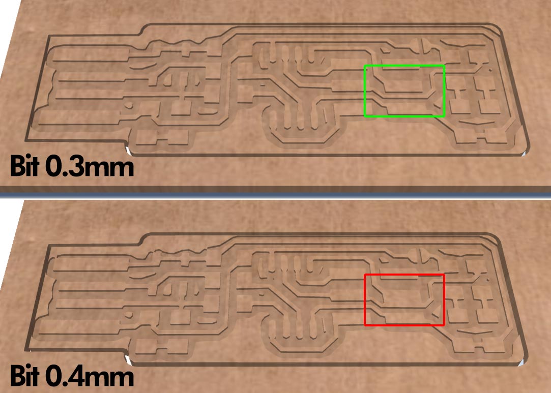
After set the surface, i set the Bit, i will start to use a Bit of 0.4mm. Can add more or edit your bits.
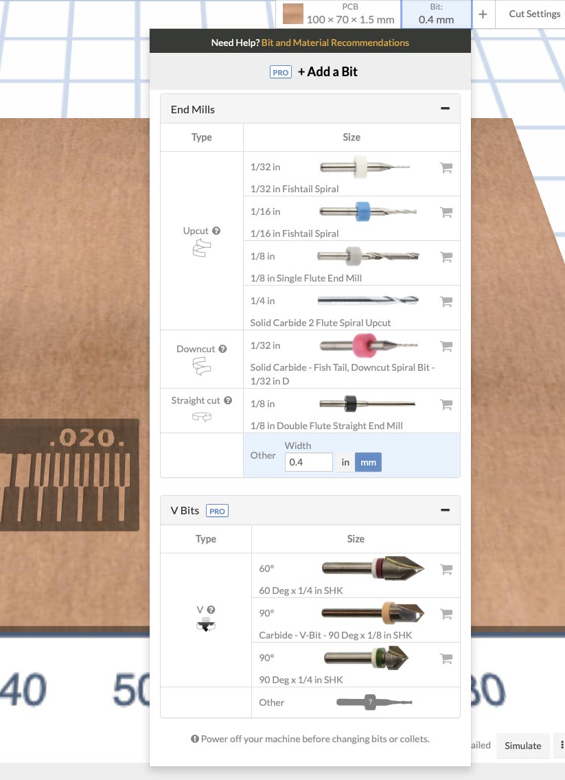
And finally set the cut settings, in my case with a Feed rate of 70mm/min, Plugge rate 40mm/min and a depth per pass of 0.15mm.
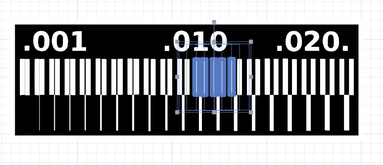
To define what the piece should cut, we must select the object to cut and define the height of the cut.
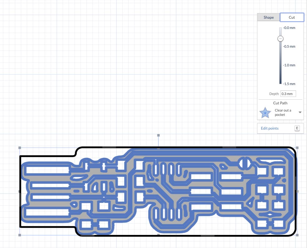
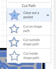
We can define how we want to cut; all the padding, cut on the path, outside or inside the path.
Start milling
I finally send the first test to be milled, it seems that it does it well, although it had a poor quality image so it did not do the correct milling.
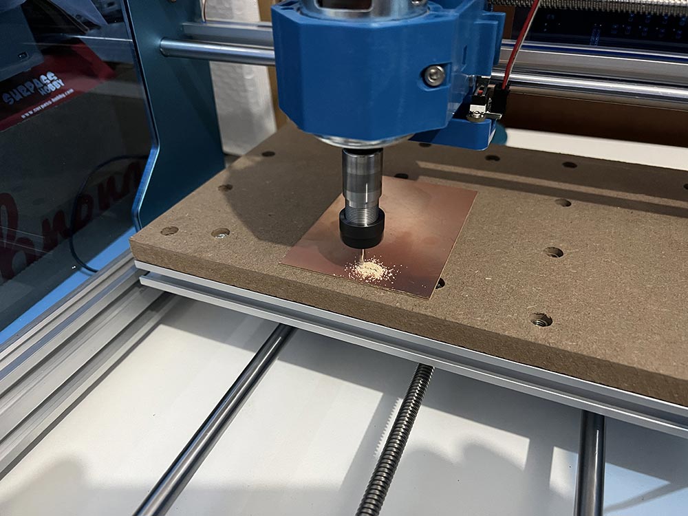
It is very important to review the preview of what the machine is going to cut, since depending on the thickness of the bit, it may cut more or less.
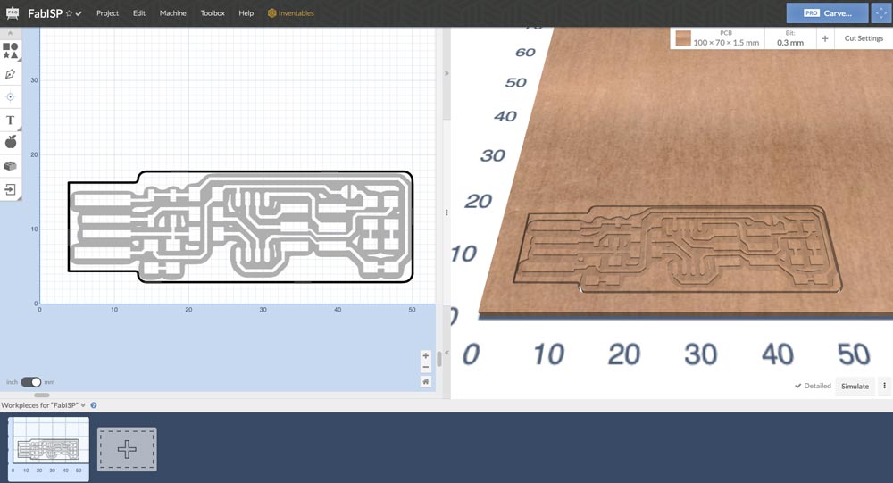
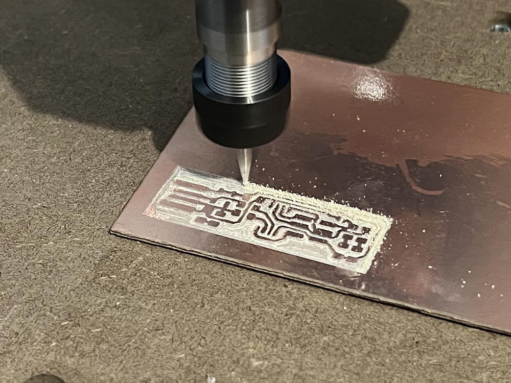
Trace width
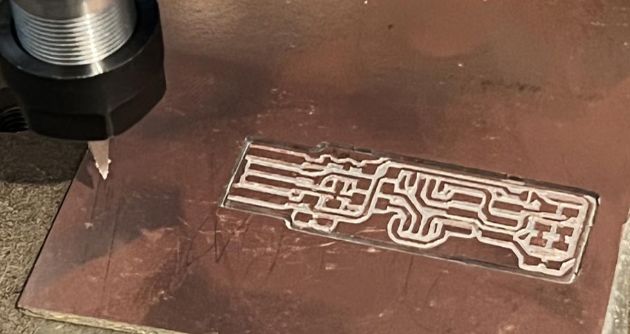
I made a test of trace with the 3018 and Easel. This is the result. I set the Bit to 0.3mm
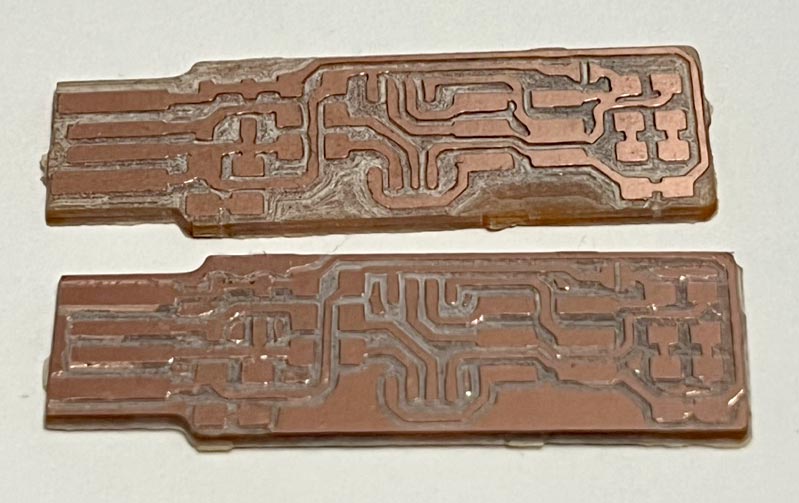
Optimizing the milling
In the case of Easel, it does nothing more than reduce the entire area, or the contours, without being able to make more passes around the area to reduce.
For this, in Adobe Photoshop I have prepared an area of passes, outside the tracks, where I am interested in removing the copper, but without having to do it for a long time, as if I were removing all the excess copper.
First need convert the image to gray scale or RBG.
For this I have selected the image channel, I have created a new channel with the original image, and I have selected it by pressing alt+channel.
So I have the selection of that channel. Then I create a new channel, expand the selection by X pixels, in my case 30, and fill it with white.
I select the original channel again, with alt+ channel, and erase with black color in the layer that was expanded. After this i select all in this channel, and copy into the background channel.
Then I do the normal process, to save the image and in Adobe Illustrator convert it to svg.
Individual assignment
Last week, during my stay in León, my instructors gave me the material to complete the first part of the assignment. A milled PCB and the components to solder. As the cnc still had to be assembled and configured to start manufacturing my PCBs, I started with the soldering part, to keep up with the class, without having to encounter the complications that putting the machine to work could entail.
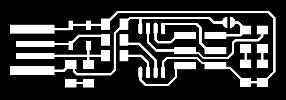
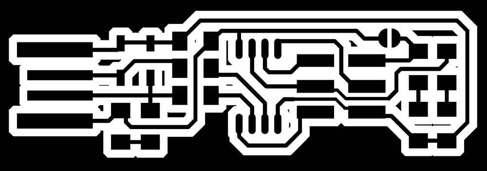
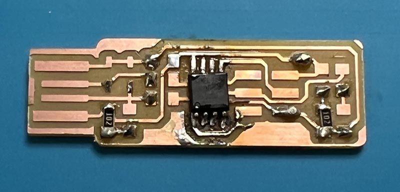
Once I had seen the design of the project and what material had been delivered to me, I made a list of the components, to then solder them. The PCB to be welded is a FabTinyISP of Brian.
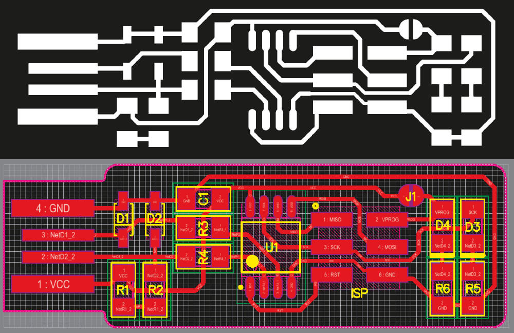
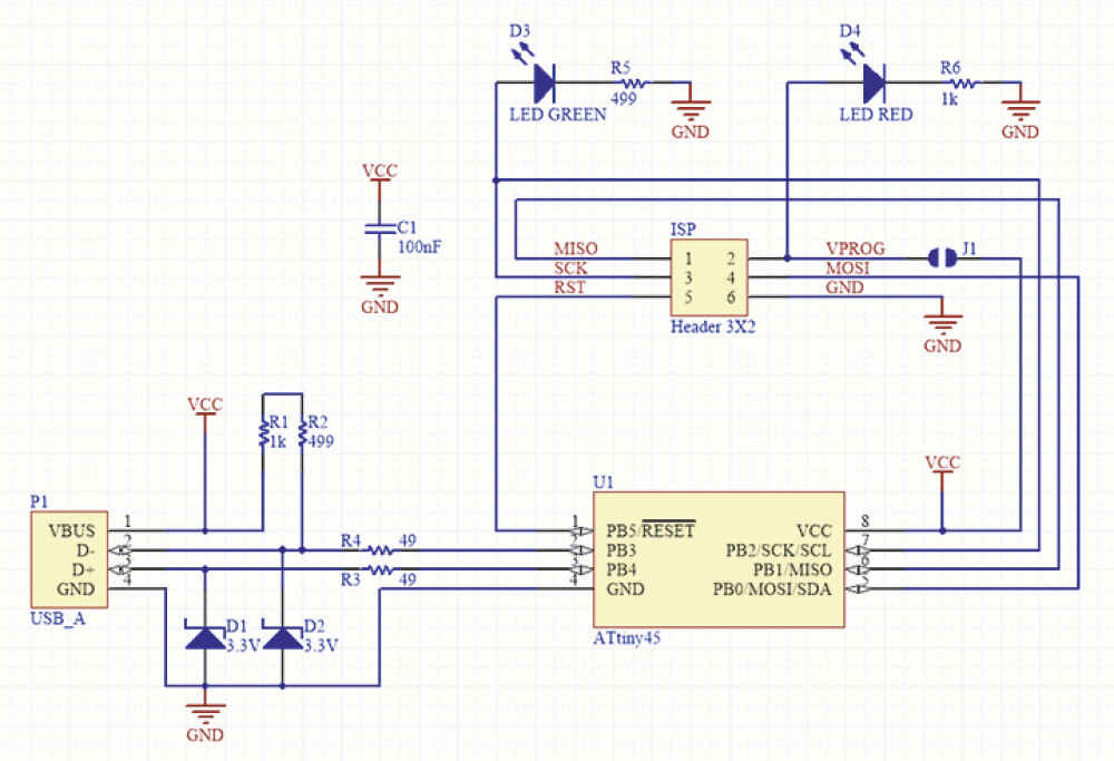
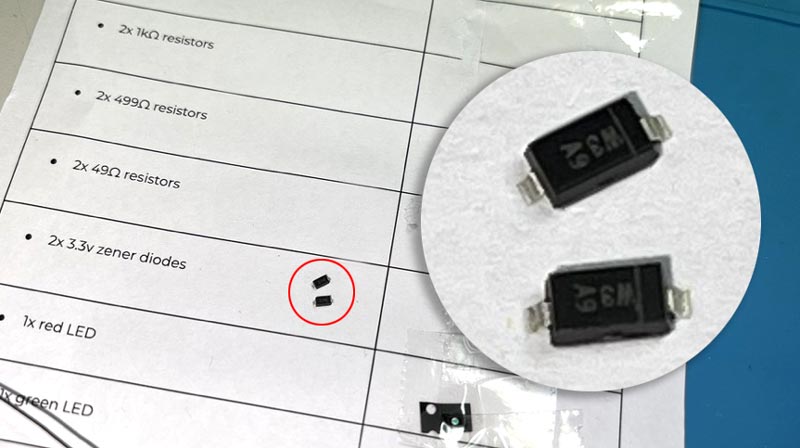
Bill of Materials (BOM)
U1 - ATtiny45
R1, R6 -1kΩ resistor
R2, R5 - 499 Ω Ohm resistor
R3, R4 - 49 Ω Ohm resistor
D1, D2 - 3.3v zener diodes
C1 - 100nF capacitor
D3 - Led Green
D4 - Led Red
ISP - 2x3 pin header
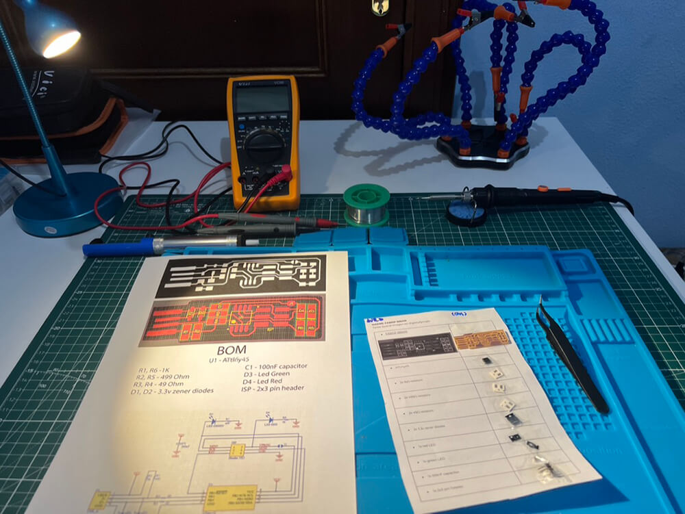
Soldering
After having all the components identified, the first thing I did was solder a point for each SMD component, where I was going to solder it initially and then solder the other points.
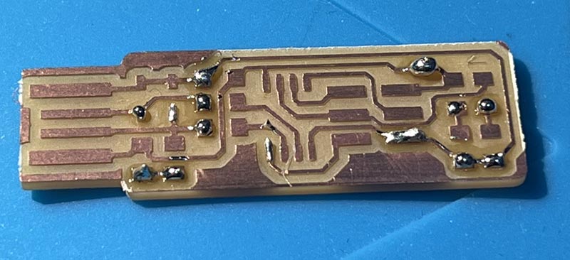
I found the ATtiny45 very complicated to solder, initially with a somewhat thick soldering iron tip, so I had to remove all the excess tin.
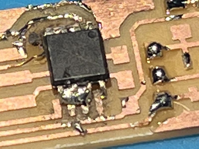
With my soldering iron it was complicated, so I went to A Industriosa, which has better soldering stations than mine at home, and Luis Miranda helped me to solder the component.
The other components were easier to solder, they were somewhat larger, although difficult to identify, such as diodes or LEDs. For the diodes help me from the iPhone camera to make a magnifying glass.
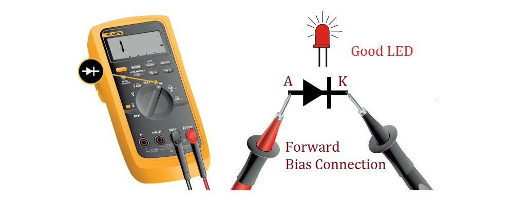
To know the directions of the LEDs, with the help of the multimeter in diode mode, identify the pole + and -.
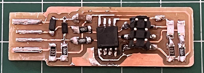
Testing PCB
For this part I use a multimeter and use continuity mode and check for shorts between VCC and GND.
Everything seems to be ok.
Program the ATtiny45
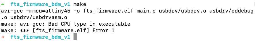
For flash the ATtiny45 i install CrossPack in MacOS 12.2 and download the Firmware for build, but when try to build gave me an error.
I have in my MacPro installed Parallels. Parallels Desktop is an application for Mac that allows you run Windows, Linux or even OS X operating systems and applications created for them on your Mac.
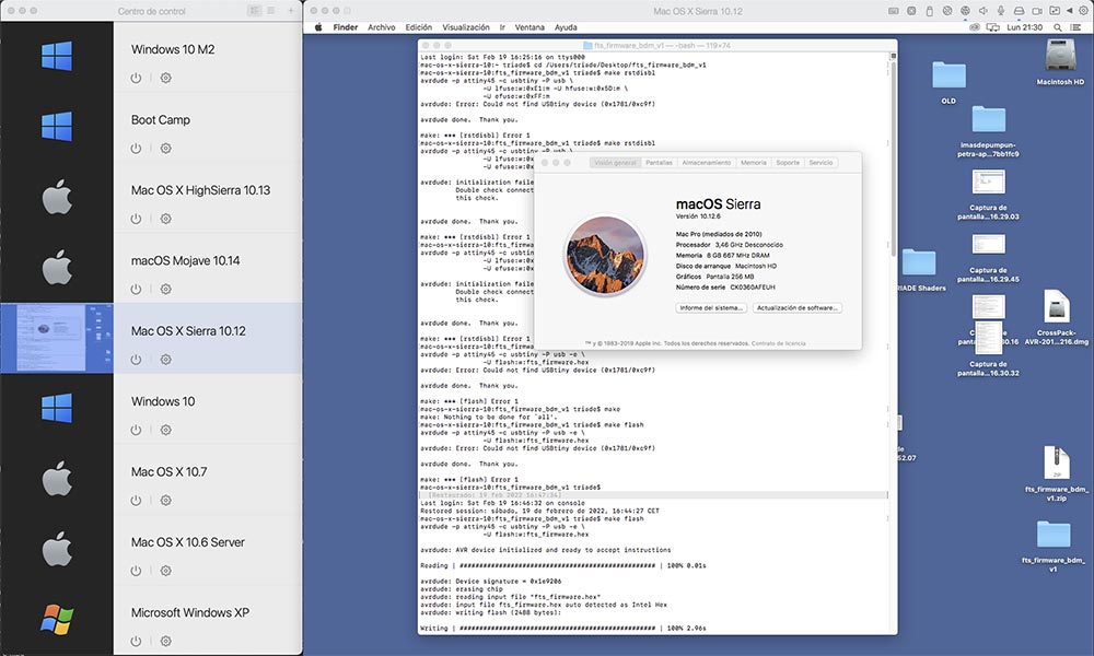
I have Windows 10, WinXP and MacOS installations that I use when I need to build an old app or use an older version of any app, or just to test something on another OS.
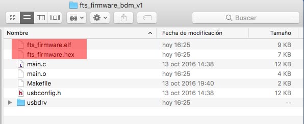
After the problems with Monterey, I try in macOS 10.12 Sierra, install the new CrossPack and try to build the firmware with make with no problems.
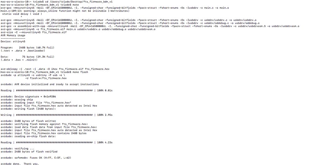
After build the firmware, i delete the content of chip with make flash
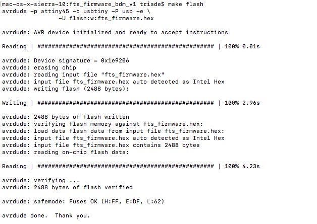
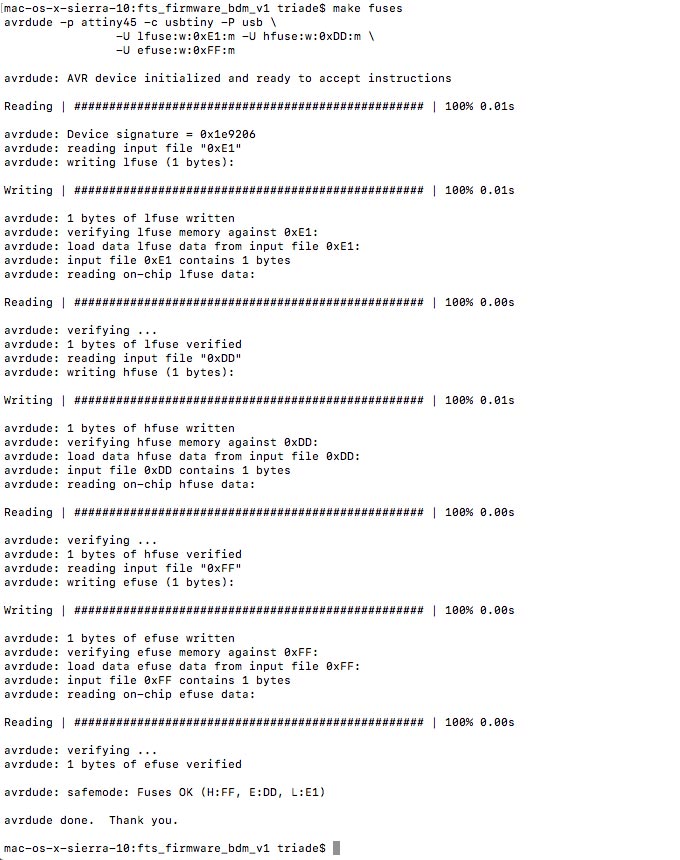
For flash the chip i use make fuse
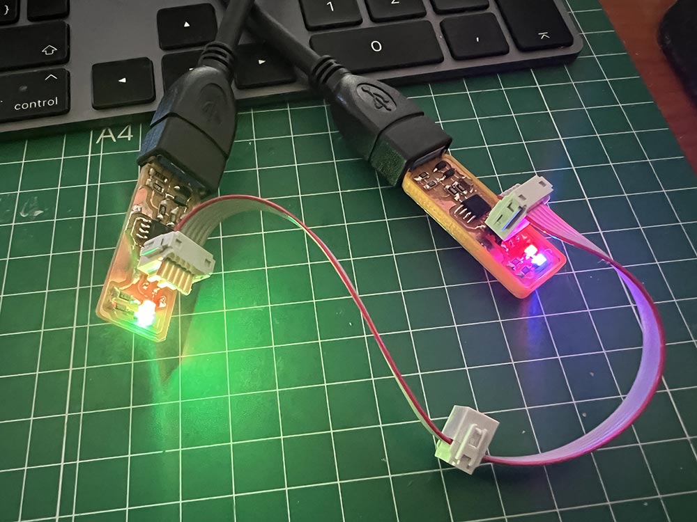
And after this i connect to Mac to see if the computer recognizes the board.
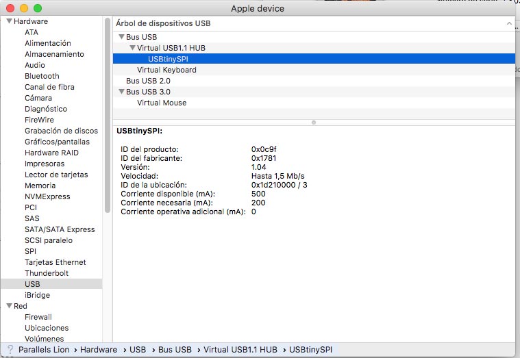
One very interesting thing about Parallels is that when connecting a device it allows us to select which Host we want to use it, whether our computer or the virtualization we are using.
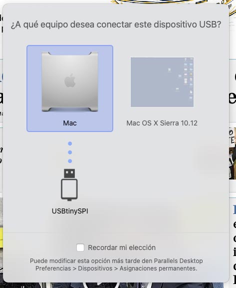
However, once the host is selected, we can certify that it is connected from About this Mac> System Report> USB
Lastly I connected the ISP programmer to the computer to run make rstdisbl. This does the same thing as the make fuse command, but this time it will also include that disable reset bit.
Downloads
Assembling Fabisp Brian (.pdf)
PCB Fabisp include .png and .svg files (.zip)
Explore more like this
17 - Invention, Intellectual Property, and Income
This is the last week before I present the final project, I already have a slide and video proposal of my project.
16 - Applications and Implications
Propose a final project masterpiece that integrates the range of units covered, answering: