
Assignment 7 - Electronics Design
Assignments
Group Assignments
- Use the test equipment in your lab to observe the operation of a microcontroller circuit board
Individual Assignments
- Redraw an echo hello-world board
- Add (at least) a button and LED (with current-limiting resistor)
- Check the design rules, make it, and test that it can communicate
- Extra credit: simulate its operation
Group Assignment
What we did in this weeks Group Assignment can be found here.
Individual Assignment
Redraw echo Hello World board and add (at least) a button and a LED
This Assignment was not very easy for me. Apart from the Cat-ISP I did for electronics production, I had no real experience with electronics. The whole lecture consisted of so many new things I havent ever heard or have thought of differently before. Like, I knew that there were some things called capacitors and resistors, but I never really knew what there job was on a specific Board and how one would choose the right values. With the local lecture on thursday this changed. We learned so many things. We went through the process of creating a whole board design with different features whilst explaining the thought processes and mathematics/physics behind almost everything. I had a really hard time grasping the concepts, but what made it easier for me to understand was the analogy with a body of water. That made things quite more clear for me. I have yet to understand everything but at least for now I could go forth and start creating my own board.
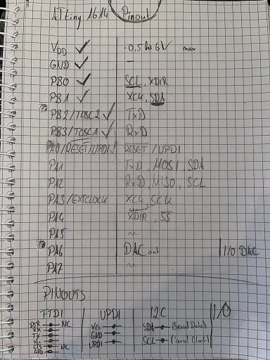
My first idea was to combine the thought of my Cat-ISP from electronics production week with this weeks assignment. As I already wrote in the electronics production week documentation, I had a few Ideas that just could not be done in time for that week. So I once again set out to create a board in the shape of my pixelated Cat I created in the beginning. Since this board would not need a USB-Plug, I simplified the Tail of the Cat within KiCad. This feature of KiCad was very cool. You can just drag around on Edged and Sides of your imported SVGs until you get to the desired shape. I did this for the Tail of the Cat, so that it would have a more natural form than the USB-Plug Tail. After that it was time to decide what microcontroller to use. Ahmed showed us a few examples of Boards from previous students and told us to go and have a look at their documentation, so we can better decide on what microprocessor to use. Pretty early on I set my eyes on the ATtiny1614 as it had many functions and pins to use for a multitude of different things. You could create a board that has a FTDI, UPDI and I2C connection, all on the same board. As I reassured my choice with Ahmed it also came up that this microcontroller had a few pins which could send PWM-Signals. This would be perfect as my final project would need motors that can be turned with such signals. After deciding on the microcontroller I tried to read as much into the documentation of the ATtiny1614 as possible. With the help of the documentation of former student Jefferson Sandoval I went ahead and started to write down what each of the pins of the ATtiny1614 would be capable of and which of the Pins could be used for different apllications like FTDI or UPDI.
I quickly realized that the documentation would stay as an open tab in my browser for the duration of the assignment. So many upcoming questions can be directly answered here. On the other hand its quite complicated to find the answers to your questions if you dont quite know what to search for in the documentation. After reassuring with Ahmed that I understood most of the things correctly, I began working on the board in KiCAD.
First things first I had to import the Fab-Libraries into KiCAD. The process for this is pretty much
straight forward. You just need to download the Git repo and extract it into a folder of your
choice. To find it better and have a consistent strcuture we were encouraged to put our libraries
into our documents folder, where KiCAD already craeted a folder for projects and other stuff. After
extracting the .zip file into the documents folder, I just opened it, cut out all files and pasted
them into the folder above, to not have just folder in folders. After setting up the files, you just
need to tell KiCAD where to look for them and what to use. This is done in three Steps, which can
all be found under the Preferences tab within KiCAD:
- Setting up/ Configuring the path to the folder you just established
- Choose a name for the path
- Give KiCAd a path to your Folder
- In my case just go to
Documents > KiCAD > Libraries - With the
LibrariesFolder selected, just press okay - Add the Symbol Library to KiCAD
- Again choose a name for the library
- Naviagte to the path of the library you downloaded
- Highlight the
fab.libfile and press okay - Add the Footprint Library
- Choose a name for the libaray
- Navigate to thr path of the library you downloaded
- Highlight the
fab.prettyfolder and press okay
If done correctly, everything should be set up and you can use the symbols and footprints of the fab library.
After setting up the library I created a new project and opened the schematic editor. From my
research and from talking with Ahmed, I now knew what parts I needed on the Board. If you want to
have a look at the BOM you can just click here. I
created this interactive BOM by installing the
Interactive HTML BOM extension via KiCADs Plug-In and Content Manager.
With this list of compoenents I went ahead and started working in the Schematic Editor. To insert a
specific part, you just need to press the Add Symbol button, which will then open a new
context menu. Here you can search for the name you gave your symbol library while adding it to
KiCAD. In my case this was fab. Now everything insode this library will be shown. If
you want to search within the library you can just use a syntax like
(NameOfLibrary):(NameOfPart) to find what you are looking for. The first thing I added
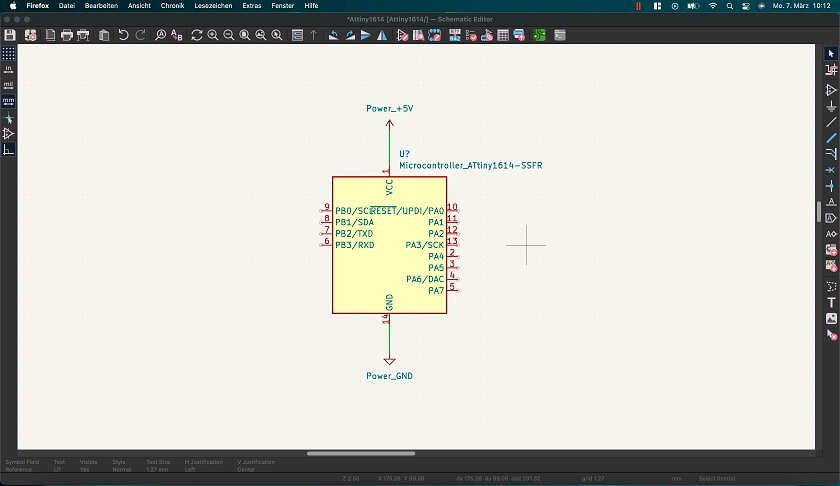
was the microcontroller which I then accompanied with a +5V and a Ground symbol. Contrary to the
other parts, the line for different kinds of volate and/or Ground can be accessed by clicking the
Add a power port Button on the right hand side of KiCAd right under the
Add symbol
Button.
After adding the microcontroller the schematic looked like this:
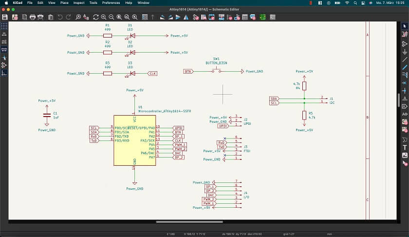
I then went ahead and added all the other symbols I needed and started connecting everything with Labels, as I think this allows for a cleaner look and does not confuse me as much when im looking at the schematic. Lables can also be created at the right side of KiCAD. After adding all the other parts, my schematic looked like this:
After the schematic was done, I ran the tool for filling in missing references in the schematic.
This
tool can be found on the top row of KiCAD. With this every reference will be numerated. So instead
of someting like C? you now have C1 or some other number when C1 already
exists. With this done I also double checked the footprints that were connected to the symbols by
using the footprint assignment tool in the top row of KiCAD. Here everything seemed fine. I saved
and clicked on the Open PCB in Board Editor Button. This opened the PCB editor where I
at first was confused, as I did not really see any of my parts. As it turns out this is pretty
normal and you have to click on Update PCB with changes made to the Schematic Button.
After running this you can now freely place the whole bunch of components from your schematic. After
the parts were placed, I followed the procedure I already did in the electronics production week and
imported my cat svg file. I chnaged the Tail as described above and slowly put parts into the cat
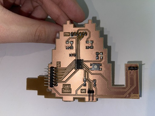
outline. The most important part for me was, that I wanted to have the microcontroller pretty much
in the center of the cat, and that I wanted to have two power LEDs which would then function as the
cats' eyes.
After putting everything down the way I wanted, I faced my biggest problem this week. Routing. I simply could not get everything to connect properly for such a long time. If everything was connected properly, some kind of Ground Isle was left over and if I managed to have the ground layer touch everything, some component was not connected. I tested around half a day until I asked Ahmed if he had some tips to fix this problem. He showed me how to efficiently use the space under capacitors and resistors to create some kind of bridges, where the ground layer could flow below the bridge. After using this advice I managed to connect everything without isolated Ground isles. The final result in the PCB editor looks like this:
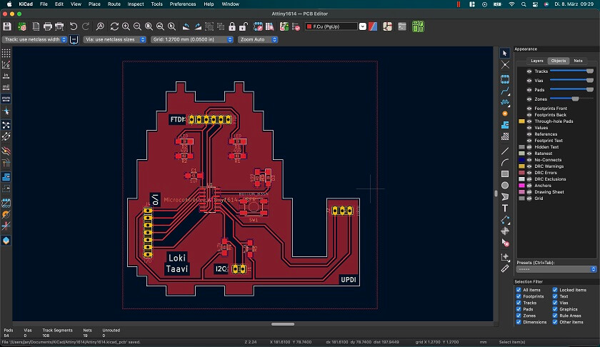
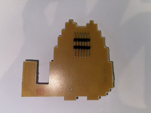
The only thing I had to change footprint wise, where the connectors for all external pins. So FTDI,
UPDI, I2C and I/O. We were told that and oval shape for the pads make thesoldering part much easier.
I edited the footprints of the pads by selecting one pad from each group and changing its settings.
The Shape would then be oval and the sizes would differ a little bit. After changing one pad you can
just use the context menu of the pad via right clicking, choosing the option
Push Pad porperties to other Pads.... This will change all the pads that are part of
the Group of the pad you changed beforehand. With the board design finished, I exported it as SVG.
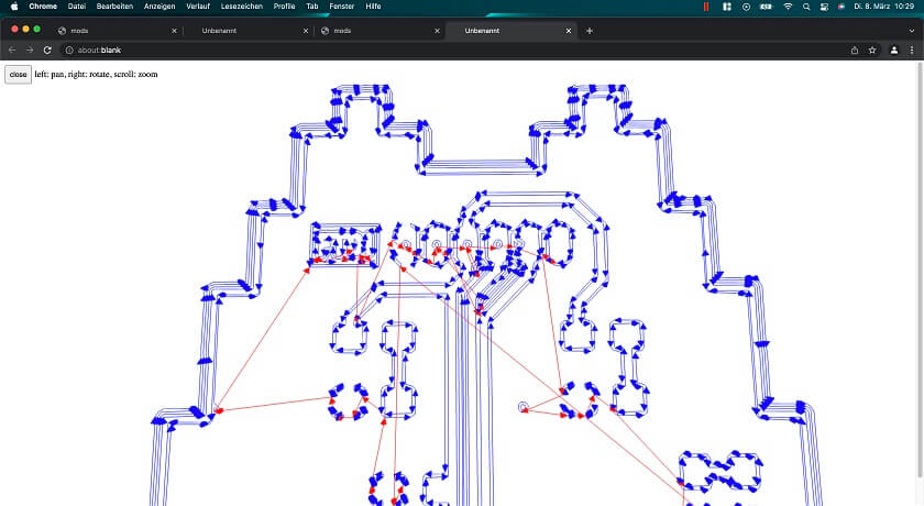
After the problems with SVG files in Mods in electronics production week, I wanted to try it again with SVGs but using a different browser. I chose Chrome, as it was the recommended browser in the lecture. I was very hopefull as opening the svg with chrome showed no mistakes in the interpretation of the SVG. After punching everything into Mods however, things started to act weird. I attached a picture below to show some of the weirdness I would get using the SVG file. So at least for me and for now, I was limited to the PNG tool. I used Inkscape to convert the SVG to a png file and then used GIMP to create my traces and my CutOut images. With these Images I opened Mods again and created the toolpaths for our Roland MDX-40.
Making the Board and testing it
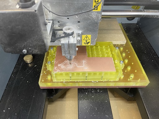
With the Toolpaths for the new Board now created I went on to the Roland MDX-40 to start cutting the Board. As in Electronics Production Week I went ahead and applied some sticky double sided tape to a copperplate and stuck it onto the acrylic layer of the machine. After that I eyeballed the X/Y Origin a s close to the lower left corner as possible and started the process of creating the Z Origin point. For this I started up the spindle and lowered it in smaller increments the closer the board was to the tool. I had a look at the tool and the copperplate all the time to see when the tool began piercing the board. When it did I set this position as the Z Origin. For the traces I used a 0.4mm cylindrical Bit as opposed to the V-Shaped Bit I used in electronics production week. For the Cut-Out I once again used a 1mm bit. After the cutting was done I was left with the following Board:
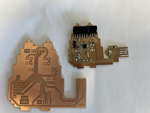
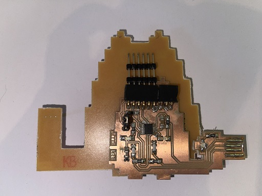
As you can see, the newer Board is quite a lot larger than the CatISP I did. This is because I scaled down the SVG to fit the proportions of the USB-A port at the Tail, which I did not need to do here. With the board cut I once again settled for the Proxon drill in the Lab to drill the holes for the pads manually. After that I gathered all the material I needed according to the BOM. This time around soldering was somehow much more straight forward than with the CatISP. There are still some points on the board that could have been soldered better but all in all I was very pleased wit my result. The ATtiny1614 is larger than the FTDI chip of my programmer, and so it was much more easy to solder each leg of the chip individually. Funnily enough one of the hardest parts was the button. Here the legs have to be straightened out as they come flush with the casing from the factory. This resulted in me trying to straighten out all the pins in the same way, which did not really work out. I had to use a bit of pressure to get a few of the legs down onto the copper layer for soldering. After the soldering was done I double checked the Vcc and Ground Lines with the multimeter for any mistakes I could have made. Everything seemed to be fine. At this point I was ready to test the new board out.
Initializing and testing the Board
To start testing the Board I loosely followed the Guide from Jefferson Sandoval, which is a little bit Outdated because atleast for me some of the mentioned options are not available anymore or are atleast called differently. The first problem I encountered was, that my Macbook would not recognize my Programmer. I only tested the programmer on my windows machine and the windows PC at the lab. From the prior testing i knew that the problem was not the CatISP but rather some driver problem with my Macbook. After a little bit of research I was directed to this page, where I downlaoded the driver for my corresponding OS. After installing the driver, my Board was recognized and I could begin. I set the CatISP into UPDI mode and connected the Boards together. First little Success: The two little LEDs I wanted to have as eyes for the Cat were working! Now onto getting the Bootloader on the ATtiny1614.
First things first we need to add the MegaTinyCore to the Arduino IDE to get the IDE to work with
the ATtiny1614. This is done in just two steps. First we need to Add a URL for Additional Board
Managers under File > Preferences. Here we add the URL
http://drazzy.com/package_drazzy.com_index.json, press okay and go over to
Tools > Boards > Boards Manager... and search for MegaTinyCore. For me
personally the newest Version at the moment, which was 2.5.10 worked just fine. After the
installation process of this package we have to edit some more options under the tools sub menu:
- Under
BoardschooseATtiny3224/1624/1614/1604/824/814/804/424/414/404/214/204 - Under
ChipchooseATtiny1614 - Under
Clockchoose20Mhz internalif you have not added an external clock to the board - Under
ProgrammerI personally choseSerialUPDI - SLOWas that promised the highest compatability
With these Settings in place I connected the two Boards via UPDI and inserted the programmer into my
USB Hub. After selecting the newly added port under Tools > Port, I burned the
Bootloader via Tools > Burn Bootloader. In theory now everything should be ready to
upload a sketch. To make things easy for testing the board for the first time, I just copied the
sample code from Jefferson
Sandovals page and laoded it onto my Board. To my very surprise, it worked! Here is a short
Clip of the LED blinking:
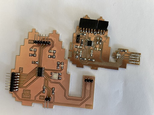
After this I just wanted to quickly test the Boards FTDI capabilities and added a serial singal that would write "HIGH" when the LED is turned on and "LOW" when it was turned off. So now in theory I could plug the Board into my CatISP in FTDI mode and open the serial monitor to see if the Board sends the Data. But there was one huge problem. The FTDI ports could not connect. As it turns out, I have not thought about the Ears of the Cat to stop my CatISP from accessing the FTDI port. After a bit of thinking Ahmed suggested that I could just desolder the current port with a hot air gun and solder a new port to the pads, that would be on the bottom of the board. I haven't really had that thought in my mind at all but I liked the idea very much. So we then went ahead and desoldered the old port, cleaned the pads up with a soldering wig as good as possible for me. After that we inserted the new Port the other way around and I just soldered the tips looking up on the front of the Board. This resulted in the FTDI port now being much more accessible:
With the new FTDI port in Place I just plugged the Board in and could read out the High and Low signal being sent by the chip: Success!

And on top of all, the new FTDI port makes the two boards look like one Board! Neat!
File Downlaods
ATtiny1614-CutOut.png)
ATtiny1614-Traces.png)