Week 6 Electronic Design

Assignments:

Group assignment:

    • Use the test equipment in your lab to observe the operation of a microcontroller circuit board (in minimum, check operating voltage on the board with multimeter or voltmeter and use oscilloscope to check noise of operating voltage and interpret a data signal)
    • Document your work (in a group or individually)

Individual assignment:

    • Redraw one of the echo hello-world boards or something equivalent, add (at least) a button and LED (with current-limiting resistor) or equivalent input and output, check the design rules, make it, test it.

-Drawing board as a shape + barebone setup + led + buttons + pin headers.
-Check DRC.
-Use the ISP toolchain to program an ISP board → hello echo,

Learning outcomes:

    • Select and use software for circuit board design.
    • Demonstrate workflows used in circuit board design.

Weekly practices:

Research

This week was intense as I had to delve into electronic components, resuming my week4’s research on microcontrollers. I explored the different types of microcontrollers. Thanks to my instructor Mr. M Kamel who suggested this useful link which describes in great detail about microcontrollers and their types.
1- Microcontroller Types According to the Number of Bits: The bits in the microcontroller are 8-bits, 16-bits, and 32-bits microcontroller.
2- Microcontrollers Types According to Memory Devices: The memory devices are divided into two types, they are

    • Embedded memory microcontroller.
    • External memory microcontroller.

3- Microcontrollers Types According to Instruction Set: CISC/RISC
4- Microcontrollers Types According to Memory Architecture: The memory architecture of microcontroller are two types, they are namely:

    • Harvard memory architecture microcontroller.
    • Princeton memory architecture microcontroller.

5- Microcontrollers Types: There are different microcontroller types like 8051, PIC, AVR, ARM,

image

I moved on to power. The MCU circuit will need electricity to operate so the powering circuit will provide the proper power to the circuit. There are AC, batteries, DC sources along with regulators to provide the proper power to the circuit. It is highly recommended to check every component’s data sheet for knowing the range of operating voltage/current.
Example: according to the Attiny44 data sheet
Operating voltage: 2.7 - 5.5V for Atmel ATtiny24/44/84

image
image

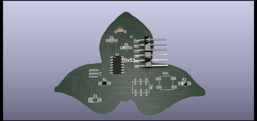
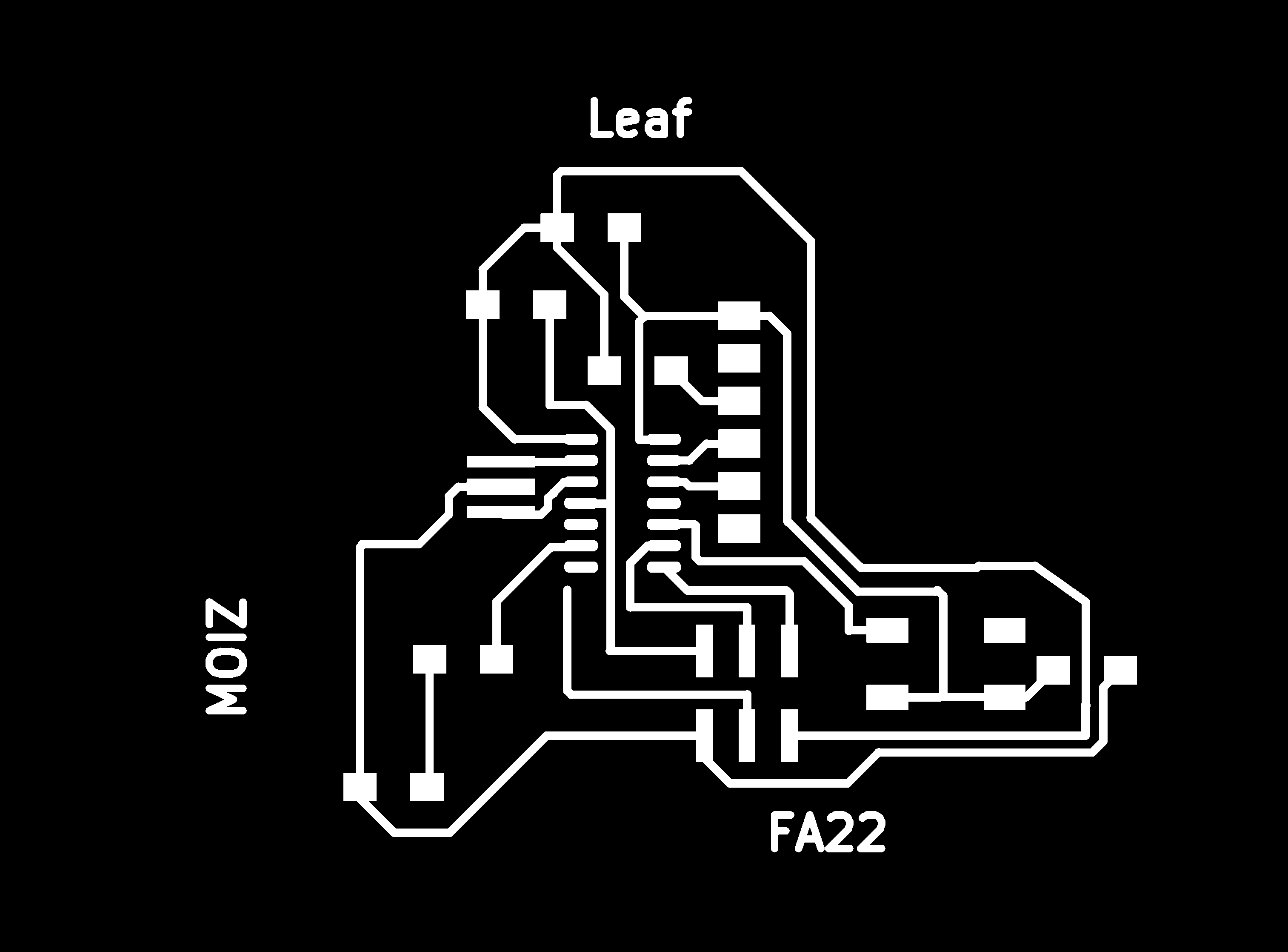
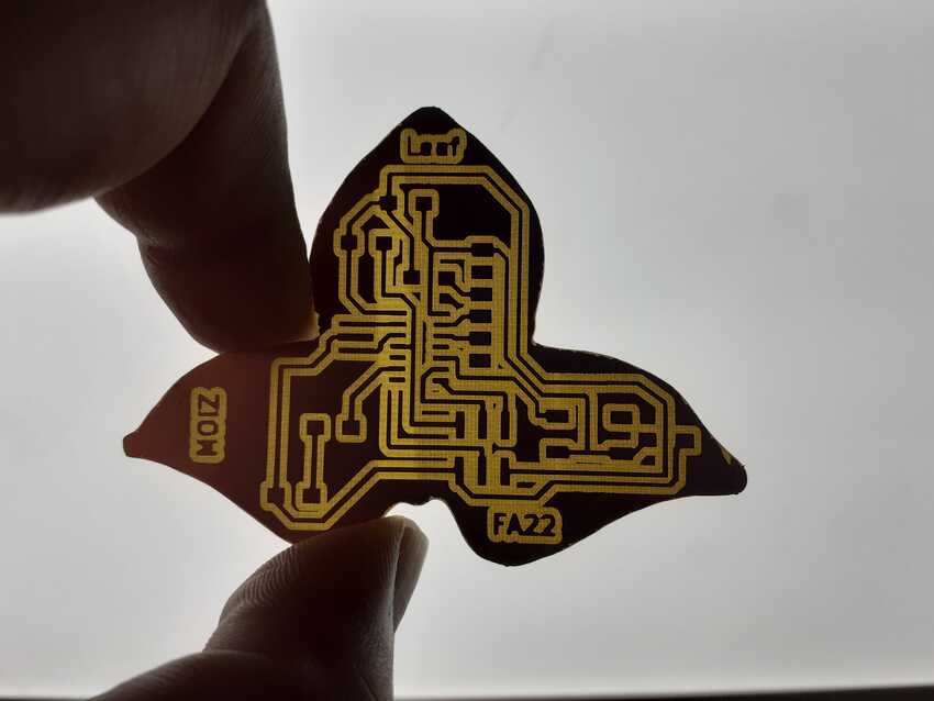
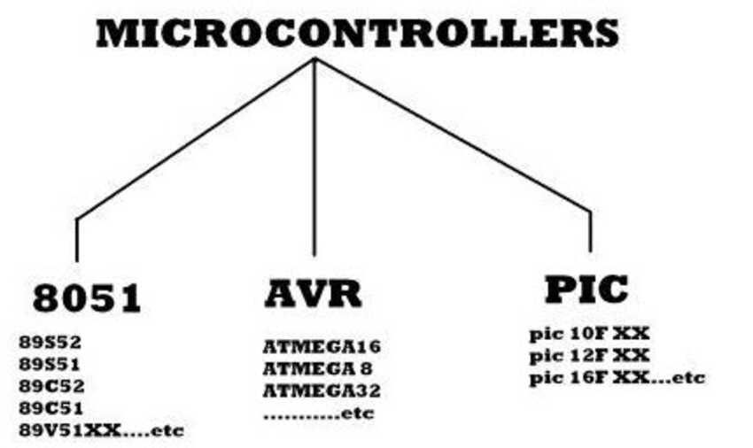
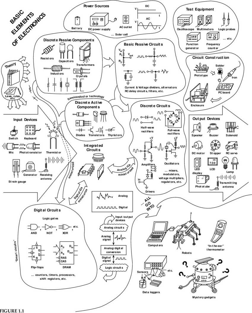
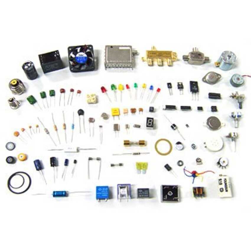
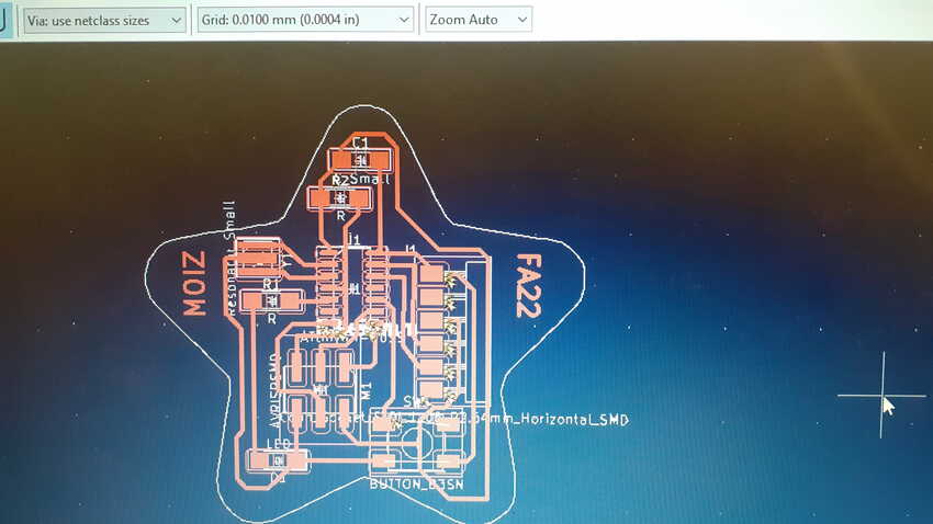
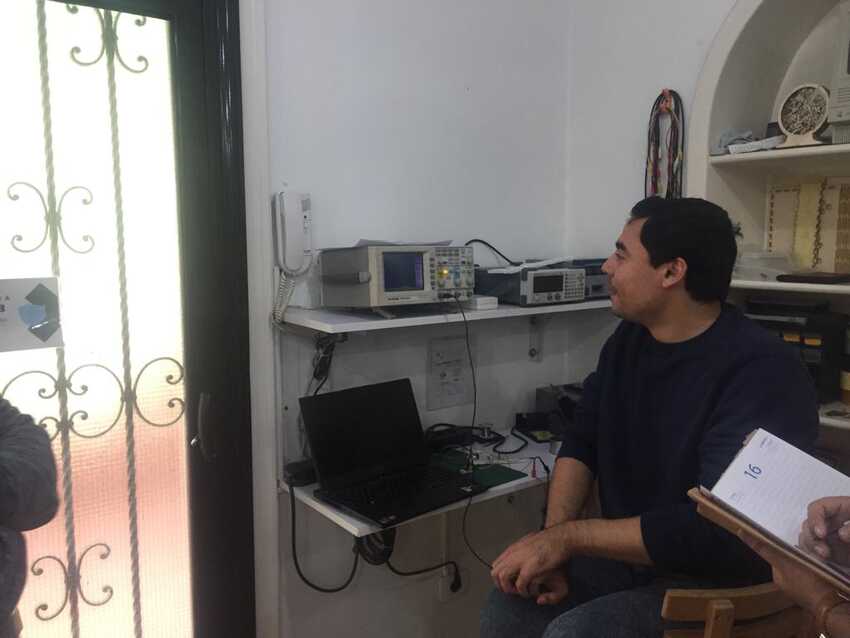
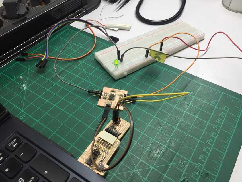
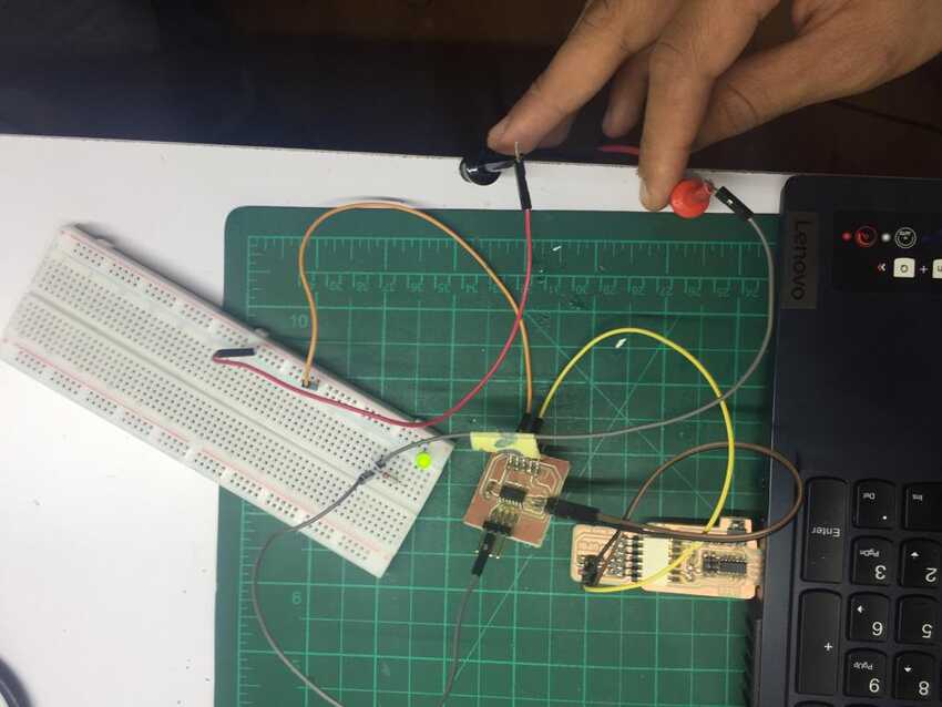
The circuit consists of many components such as active and passive components (as shown in the picture). It was recommended by my instructor to have an overview of as many types of components as possible to grasp the electronic designing well.

So I started with basics: Resistors: as the name suggests, create a resistance of the electrical flow. They have two end points and have no specific orientation (they are non-polar). In every circuit there is a balance between voltage, current, and resistance so that the resistance is the voltage divided by the current: R = V / I. This is a very useful video for beginners to learn more about the resistors and its types.

capacitors: Capacitors store electrical charge, somewhat like a battery, although it’s stored in a different way. Generally, it can’t store quite as much energy as a battery, however it can charge and release its energy much faster. Capacitors stay charged for a little while even after the power source is cut off.
The unit value of a capacitor, its capacitance, is measured in farad, given by the symbol F. The values used on our boards are generally really small, around micro, nano, and pico values. They can be used to smooth out noise in the power supply (such as when converting from AC to DC power). It basically helps to keep a constant voltage throughout the circuit.
SMD capacitors are tiny rectangles with a color that signifies its capacitance value, while for THT capacitors you can have several different kinds of shapes, such as cylinders and flattened spheres, with the values written on top. For all beginners like me I highly recommend watching this short video about capacitors.

Diode:A diode has an anode (positive) side and a cathode (negative) side, with the current being able to flow from the anode to the cathode side. A diode can thus (functionally) only be installed in one specific direction. Generally, the cathode side of a diode is marked somehow, such as a white line or an arrow mark on the bottom side.
LED stands for light-emitting diode. It’s a specific kind of diode, but one that’s become more “famous” than the “normal” diode. An LED emits light when current flows through it. However, a diode is a component which allows the current to only flow in one direction. diodes can be used to protect a circuit from accidentally connecting a power source in the wrong direction, and to help go from AC to DC current. But LEDs can of course be used simply to have a (blinking) light.
Besides LEDs we could also come across Zener diodes, which allow you to clamp a voltage (say you want the voltage to not get higher than a certain value).This video helped me to understand more about it diodes and its properties.

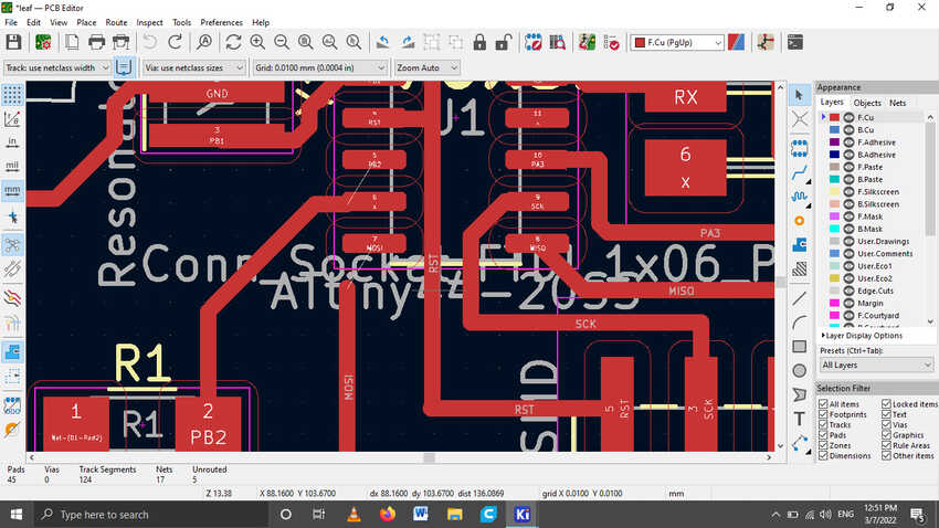
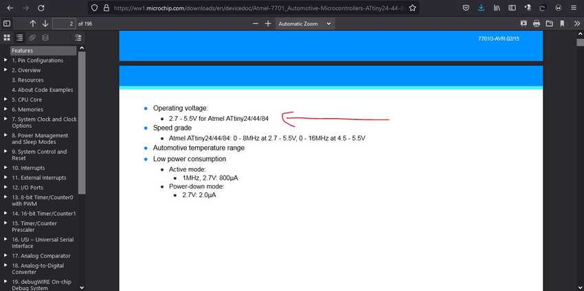
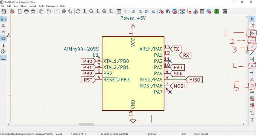
Resonators: Resonators are used as clocks inside a circuit. They are a critical part of a microcontroller. They have a piezoelectric material inside, such as a quartz crystal, that resonates at a certain frequency when a current is passed through. For the old ATtiny44 chips the internal clock wasn’t accurate enough and thus an external resonator was needed. You can clock a microcontroller using a crystal oscillator and two capacitors or a resonator. We usually prefer to work with a resonator since it does not need additional capacitors.
There are many components left to discover, Stay tuned for more updates after finishing my assignment.

image
image

Kicad

I resumed my practice from week4 and continued the tutorials. I also explored how to add a footprint mainly because I wanted to explore how to add customized design for the outline of the pcb . This video helped me alot and I followed it to prepare a non-geometric shape like a star and practiced designing on it. Voila here is the result.

image image
image

UPDI Programmer

In week4 I fabricated 2 boards, bridge and serial to UPDI for programming purposes but couldn’t finish it, so we took the opportunity this week and completed all the process so that in the future we don’t get constrained to fabricate it with the other assignments.
All the steps are updated on week4 assignment page

Simulation

I explored the simulation on Kicad software at first I attempted to do it all by myself without any tutorials and as expected did not work then I followed this video and found that it worked and now I will explore more and keep updating here. ins

image image

Weekly assignments Group assignmnts:

Here is the link to the group assignment page.
This week in our group assignment we explored the test equipment - Oscilloscope, which observes the operation of a microcontroller circuit board.

image
image

The Multimeter is a measuring instrument that can measure multiple electrical properties. A typical multimeter can measure voltage, resistance, and current, in which case it is also known as a volt-ohm-milliammeter (VOM), as the unit is equipped with voltmeter, ammeter, and ohmmeter functionality. Some feature the measurement of additional properties such as temperature and volume.
Analog multimeters use a microammeter with a moving pointer to display readings. Digital multimeters (DMM, DVOM) have numeric displays and have made analog multimeters virtually obsolete as they are cheaper, more precise, and more physically robust than analog multimeters. It is commonly used so that is why I didn’t focus on this more but I concentrated on something which I haven’t seen in my life, this was the first time I heard about it and explored how to operate it.

image
image

The oscilloscope graphically displays varying signal voltages, usually as a calibrated two-dimensional plot of one or more signals as a function of time. The displayed waveform can then be analyzed for properties such as amplitude, frequency, rise time, time interval, distortion, and others. Originally, calculation of these values required manually measuring the waveform against the scales built into the screen of the instrument. Modern digital instruments may calculate and display these properties directly.

image image
image

Our instructor had prepared a pcb attiny1614 and used the UPDI programmer with FTDI serial communication board to program it to automatically increase and decrease the voltage on the led , the result can be observed by the light intensity but for accuracy we used the Oscilloscope machine to view the voltage change in specific time period (as in technical terms signal reading of changing duty cycle of a PWM signal overtime). The graph which displays signifies the signal voltage which is read between the led ( 2 probe is connected to the 2 ends of the led).
I was amazed when I found out that this machine’s importance in regards to reading the time and debugging the error in any voltage related problem.

image
image

Individual assignmnt:

For my individual assignment I had to redraw one of the echo hello-world boards and use the ISP toolchain to program an ISP board. Considering the limited resources available in the lab and recommendation by my instructor, I used the “ATTINY44” , redrawing attiny44 echo hello-world board and customized it by adding new components and the border shape. In this documentation I will be focusing on Kicad software more as it was the new and required learning output from this week. And the other fabrication and programming steps will be discussed in less detail.
For the outline pcb shape I wanted to explore my capabilities by not just downloading it from the internet but to DIY it also. So, I came across this lovely 3 leaves design on someone’s main door and got inspired by it and tried to replicate it as perfectly as possible.
As practiced in week2, I used both raster and vector applications Gimp and Inkscape to trace the image and finally got the result which I wanted to fill the 3 leaves with black color and the rest white so that the Kicad image converter would read it correctly.

image
image

I prepared my Kicad software by following Prof. Neil’s video and added fab2022 libraries for both symbol and footprint by navigating to their editor options and adding the files in there.
I also defined the design rules from the PCB window from the files menu board settings and then navigated to the design rules on the left and changed all the values to “0.5mm” so that I can get some space to solder easily.

image image image
image

Then I opened the image converter from the Kicad dashboard and converted my 3 leaves design. I found this tutorial very helpful and very detailed.
After loading the image by clicking on the load bitmap. I changed the required settings (size, layer and footprint mod file) as shown in the picture above.
Then I changed the layer name in the mod file and saved it in a folder ending with “.pretty” so that I can add it in the footprint in the Kicad software.

image
image image

Then I moved on to the schematics of my board. Since I've been practicing on this software from week4, I knew the basics and could manage the basics very smoothly. That’s why I explored some new tools this week in Kicad. All the tools which I used are numbered in the image.
1) Add a new symbol: By pressing on the icon or the shortcut A on the keyboard I added each component from the fab2022 library and its footprint to have the correct symbol and footprint. For example, in the add options I searched for the library and scrolled down until I found LED which I wanted to add as an extra customization. Upon highlighting the LED option the symbol and the footprint is previewed on the right side which helped me to choose and understand about it quickly.
2) The second icon I explored was a kind of special power symbols for VCC (each volts..), GND and power flag ( which helps in indicating input or output for the power). These are special symbols to resemble power related operations on the board. I used the +5v as a source of power VCC as the board will be connected on the computer via usb cable and the normal GNd symbol for the ground tracing. As for the power flag I placed them on the FTDI and ISP connectors so that the board's power input and output is known from these pin headers.
3) This icon activates the net routing line and the shortcut is W on the keyboard, this allows me to join any connections and pins together. As shown in the schematics pictures the green line is this net routing line.
4) This is a new tool which I explored this week that if any of the pins on the components are still not connected with anything this icon acts as “no connection flag” so that in the ERC check it doesn't consider this as an error.
5) I used the labeling process to join the connections with each other because it looked more neat and easy than running along with a long net routing line. It is a very simple and easy to use tool, just add a label and type the name and click ok, same for the end point so that it connects together very well.
By using these tools I designed my whole board. Here are some pictures of the schematics.
Tip: The name in the label should be exactly the same on the other end of the connection, to get a successful connection between them.

image image image image image
image

After finishing the process I first clicked on the annotate to give all the components its name automatically. I.E. for the resistors it automatically numbers them by R1, R2, R3 and R4. In short it gives names to each component so that it helps identifying it anytime.
Upon completion I clicked on the ERC check icon which is located on the top bar. If there are any errors or warnings it will show in the popped up window, if not then move on to the next step. (the errors are visible in the DRC check)

image
image

On the top there is an icon which opens the pcb window where I can actually design the pcb and arrange the components on the specified outline. At first the components didn’t show as my pcb window was already open so it didn’t update, so I pressed on the “update from the schematics” icon which updated all and now all the components were visible. Here also I used many tools ( I didn’t mention the simple and basic tools rotate and move tool ).
1)It is the same as adding the symbol but here to add the foot print. I used this tool to add my 3 leaves design in my design workspace. All other footprint of the components were already allocated in the schematics that is why I didn't need to add any components anymore.
2) Routing wire line which results in the traces on the pcb board is activated from this icon or from the X letter from the keyboard. And to finish it by pressing the K letter from the keyboard. This part is the most interesting and exciting to do the main designing of the pcb connections but at the same moment it is the tedious job to perfectly join the components all together in a small area without using any kind of extra components which acts as the bridge (not via or bottom layer as I am still focusing on single layer pcb only on surface mount components). I guess I need more practice and exposure so that I reach this stage.
3)This is the text tool from which I wrote on my board my FA22 and my name and the name of my outline pcb design LEAF.
4)This is the measuring tool where I checked that the components are far from the outline of the pcb by at least 1 mm so that while cutting it doesnt eat the traces/ pads of the components.
5)F.CU is the top layer name of my board which I am currently working on and which will be exported and fabricated from this layer’s design.
6)EDGE.CUTS is the outline pcb layer where the lines color is white and where I added my 3 leaves’s design to automate the 3D shape of the pcb.

image
image

By using these tools I completed my design and moved on to DRC checking. Here I encountered many warnings and errors about silkscreen and overlapping, which as a beginner it didn’t matter to me very much as I was not fabricating with the silk screens.
Then I pressed the “alt+3” to activate the 3D viewer and view my board and its components if possible.

image image
image

As this was one of my first attempts to design and fabricate pcb on my own I asked my instructor for any comments and feedback before I fabricate , so 2 comments were to keep the resonator as close to the attiny44 as possible, so I changed the position as recommended and then exported layers by navigating to the Plot option in the file menu and then selecting the the layers which I needed “FU.CU’ and “EDGE.CUTS” and selected plot.
And the second comment was to make sure that the distance between the components and the outline minimum of 1mm. I also checked that by the measuring tool.

image
image

From now on I had use the process which was described in week 4 in more detail. That is why I will speed up the process here.
I prepared the gerbers files in gerberview and then adjusted the PNG file from GIMP to reach these 2 images below.

image image
image

I used the mods as CAM for roland mx-20 machine and fabricated my board. All the steps are briefly described earlier.

image image
image

I soldered my fabricated pcb and made it ready for programming.
To program this board I followed the programming guide from the class schedule and used my FabISP programmer which I fabricated it on week4.
I copied text from both mentioned in the notes: echo.c.make and echo.c and pasted it to a new notepad++ document and renamed it to hello.ftdi.44.echo.make and hello.ftdi.44.echo.c .
Then I right clicked in the folder containing the 2 files and clicked Git Bash here.
I typed make -f hello.ftdi.44.echo.make program-usbtiny-fuses while connecting my FabISP to my laptop and connecting it with the hello echo board using ISP 6-pin connector. At first it didn't work which I have discussed in the challenges. Then after solving the problem I retyped the previous command and after getting successful message I typed -f hello.ftdi.44.echo.make program-usbtiny.
After getting successful messages I opened an arduino IDE and opened the serial monitor while connecting my board with an FTDI cable and tested it in serial.

image image

Hooray here is the result.

image image

Voila its done

To sum up, I completed the following:

    • √ Linked to the group assignment page.
    • √ Documented what you have learned in electronics design.
    • √ Explain problems and how you fixed them, if you make a board and it doesn't work; fix the board (with jumper wires etc) until it does work.
    • √ Included original design files (Eagle, KiCad, - whatever).
    • √ Included a ‘hero shot’ of your board.
    • √ Loaded a program and tested if your board works.

File: Download KICAD file with gerber files and outline file.

#Challenges 1

While designing the PCB, I checked the DRC and it was all good, but as soon as I changed the arrangements of the components after my instructor's feedback, I didn't check the DRC again thoroughly because I missed 2 traces and didn't connect them properly. as shown in the picture.

#Solution 1

The 6th pin problem was solved easily by just changing the pin number in the coding, but the 7th pin of the IC was problematic as it wasn't properly connected. So while soldering I added a small piece of resistor leg and connected both traces together.

#Challenges 2

After soldering my pcb didn't work, I could not program or burn the bootloader on it.

#Solution 2

My instructor pointed out that the first problem was that while soldering I made a short circuit on the resonator. then still didn't work so he changed the IC itself as I may have burned it and now it's not working. and it finally worked thanks to my instructor.

image

Aknowledgment