Week 4 Electronics Production

Assignments:

Group assignment:

    • Characterize the design rules for your PCB production process: document feeds, speeds, plunge rate, depth of cut (traces and outline) and tooling.
    • document your work (in a group or individually).

Individual assignment:

    • Make an in-circuit programmer by milling and stuffing the PCB, test it, then optionally try other PCB fabrication processes.

Learning outcomes:

    • Described the process of milling, stuffing, debugging and programming.
    • Demonstrate correct workflows and identify areas for improvement if required.
    • Explained any problems and how you fixed them.
    • Included a ‘hero shot’ of your board.

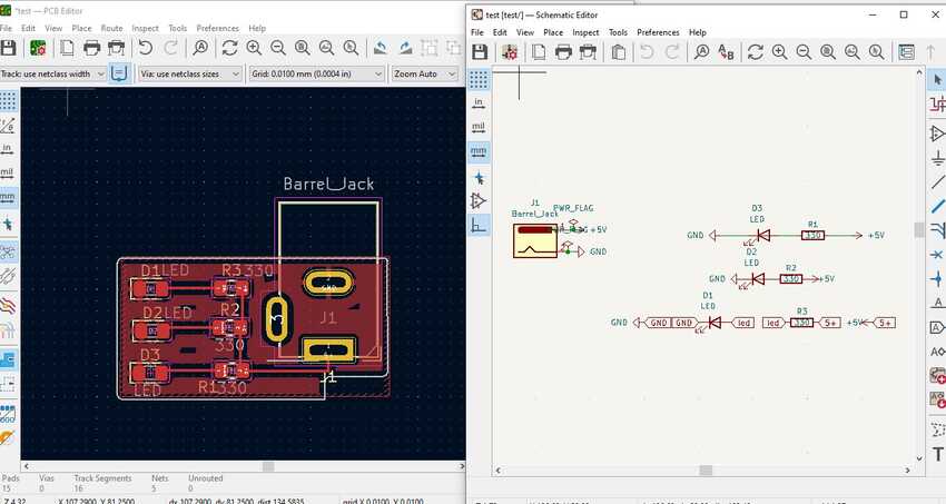
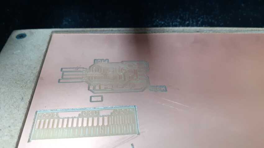
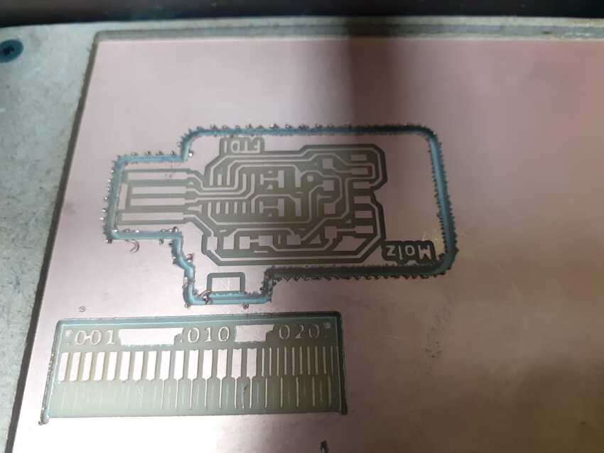
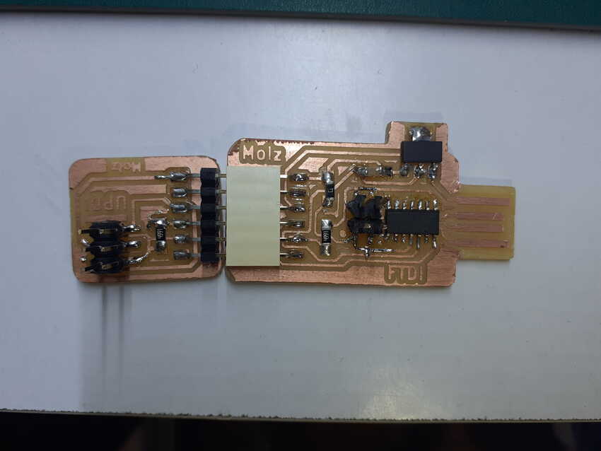
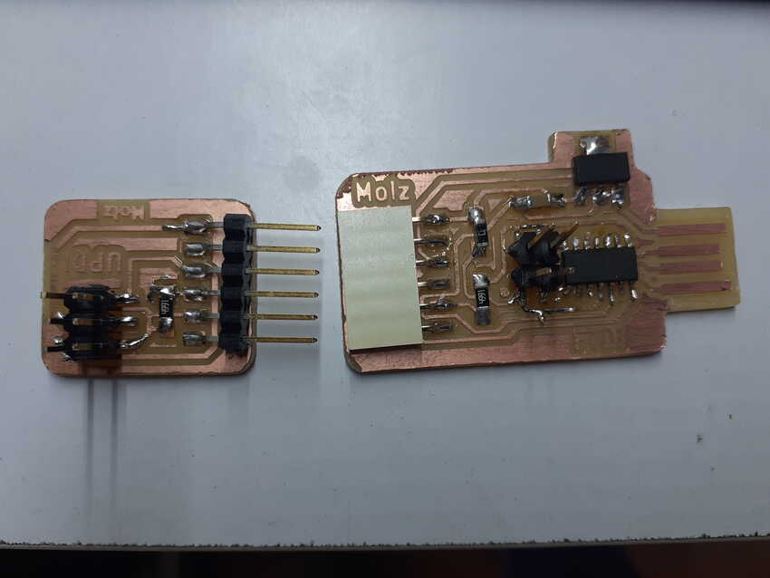
Weekly practice Research

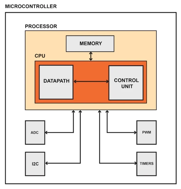
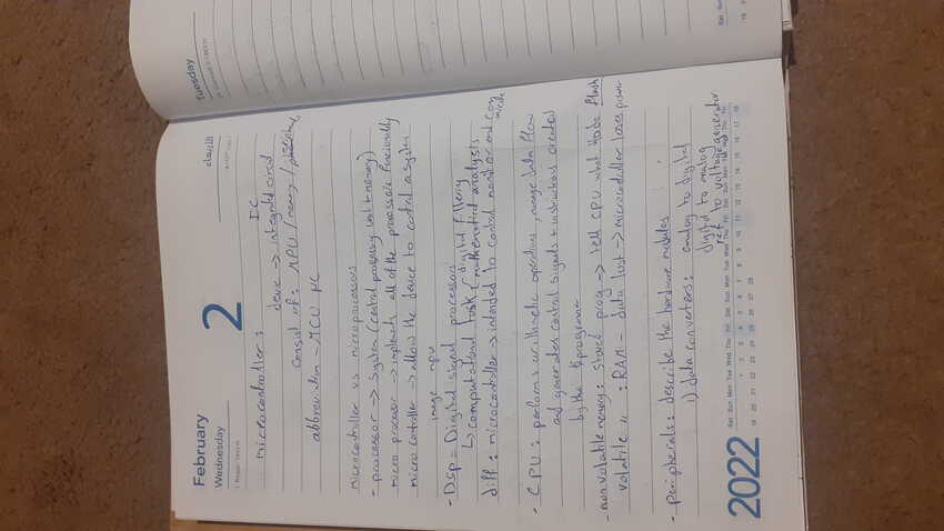
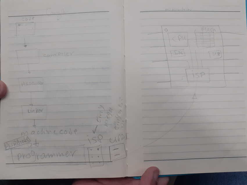
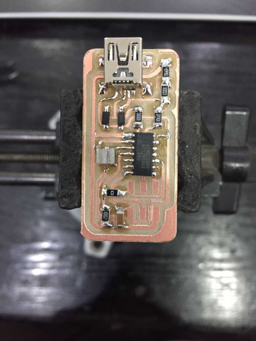
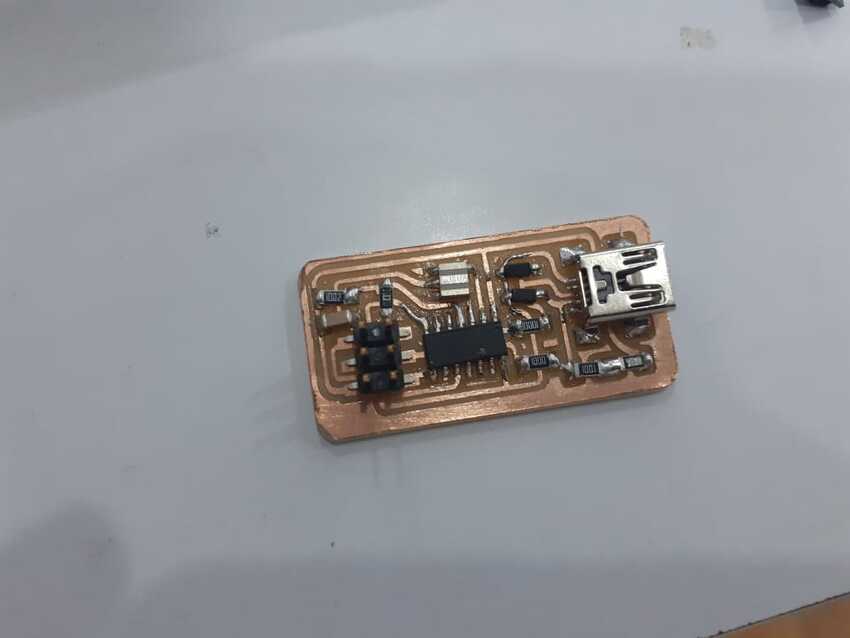
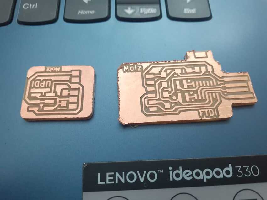
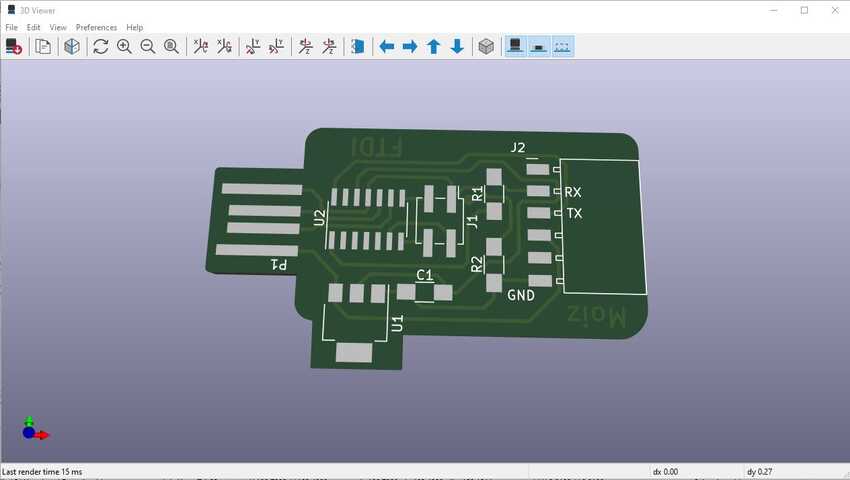
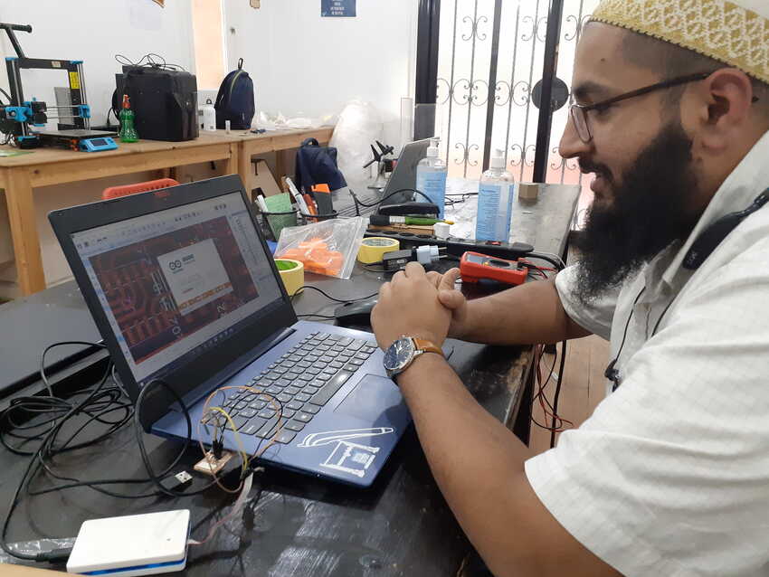
Electronics production is a whole new subject for me as my background is not engineering. I started by learning about MCU’s/microcontrollers, peripherals and a little about the families and programmers.
At first I found the terms and the concepts a little bit confusing but then step by step it all started to make sense and I was able to cope up with the little information I learned. I am looking forward to delve and explore more, but after finishing the weekly practice and assignment.
I did little reaasearch on micro controllers and peripherals and made some notes so that I can remember it well. There are plenty of recources but these were the most helpful of them all for information about microcontrollers and pheripherals.
I concluded while learning that for my final project I may need the timmer, analog to digital, input and output, serial communication and memory peripherals. As for the digital to analog and the pulse peripheral is still not chosen as no task assigned to it yet.

image image image
image

KiCad Software

I also took the advantage and started learning the designing process side by side so that it can help me in my assignment for customizing the programmer pcbs and also to ease the process in the future.I downloaded KiCad, as it is open source and easy to use software. I found these tutorials very helpful and in great detail but the only catch was these videos were for version 5.0 and I downloaded the latest version 6.0 so found little differences in the command keys and the interface. I liked the software very much as it has the option to choose any symbol for any footprint i.e. if i want to use the triangular shaped symbol without the arrows, I can easily do it in this software.

image

Weekly Assignment Group Assignment

Here is the link to the group assignment page.
This week in our group assignment we had to characterize our machines (We have 2 machines: Roland mdx20 and China Router ) at the fab lab for pcb fabrication. This process lets us know the design rules for manufacturing on these machines.The design rules are as follow:

    • Minimum clearance.
    • Minimum trace width.
    • Speed of the spindle.

So our instructor started explaining theoretically the processes which are:

    • fixturing: The pcb should be fixed by any adhesive material to make it rigid on the underlay and the underlay also should be rigid on the bed so it doesn’t move from its place. For the pcb - underlay adhesion it is recommended to use tape.
    • Underlay: it is the sacrificial wood sheet which is put rigidly on the bed. The cutting process involves drilling holes and the pcb border, so to cut them accurately the bit should be cut deeply so it cuts from the sacrificial layer also.
    • Orientation: When fixing the pcb on the underlay, the underlay should be correctly leveled and shouldn’t be any remains of the previous job, also the pcb should be aligned well.
    • Zeroing: For better communication between the placement of the pcb and the machine we should set zero for the 3 axis, X Y Z. The X and Y are done simply by commanding the machine to move certain millimeters, as for the Z, by controlling on the machine move the Z axis down until little space is left and then start the process of set-screws.
    • Set-screws: This process involves fixing the bits in the spindle and tightening them with the 2 black screws. It also involves while zeroing the Z axis to loosen the screw a little bit so that the bit should fall and touch the surface of the pcb and then tighten them back again.
    • Milling: This is the first process of the machining for the pcb, where the machine traces with V-bit 1/64 on the pcb.
    • Cutting: This process involves the drilling of the holes plus the cutting of the boundary of the pcb by End Mill 1/32 bit.

image image
image image image image

Then under his guidance we practically fabricated the test on both machines.
My role in this assignment was to partner up with my friend/colleague Amany Ayman then to fabricate this test on the china router machine . It was amazing to work with her and get to know more knowledge about how to use Mods from her for exporting gcode for the machine, then we had setup the machine for fabrication by applying tape on the pcb and cleaning the underlay well before fixing the pcb on it and then we both used the open builds software to run the machine. The process of milling was running very smoothly, actually it was kind of exciting and enjoyable to use this machine. Until the disaster happened in the cutting process :).
To know more about the disaster, please click here. I hope explaination is not needed, but still if needed Contact us (fablabegypt) on mattermost. Thank you.
So we relied on the mdx-20 results which are:
A. The minimum trace width the machine can mill is 0.001mm.
B. The minimum distance between traces is 0.42mm.

image image image

Individual Assignment

I had to make an in-circuit programmer that included a microcontroller. So I started by fabricating a FabISP programmer without any customization following Ali Shtarbanov’s tutorials.

image
image

Firstly I downloaded both images: trace2.png and outline2.png and found out that the color orientation was not proper in the outline image. As the black color indicates the cutting line and the white indicates not to cut. So I inverted the color in the image using Gimp software . I added another layer and scaled up a little bit so that the thin line of the border becomes large one- this will effect while choosing the tool diameter in the Mods. Then I merged both layers to have a result like this image.

image
image

Next step was to generate the gcode , so I opened the CAM software: Mods.It was my first time to use it, very exciting and easy to use (which I recomd to use it always) then I opened the page and then after pressing the right click on the mouse, I navigated to programs > open server program >Roland-mill- PCB png.
Then I added the file by clicking “select png file” and changed under mill raster 2D as follow:

    • The tool diameter for each traces:0.4 and outline:1.15mm.
    • The Max depth 0.15 for the traces.
    • The Offsets 3 for the traces but for the outline 1.

Then I clicked calculate to view the outline to be cut.
Then I moved to the “Roland MDX-20 milling machine” and these settings:

  • The Speed for traces kept it 4 and for the cutting process 1.
  • The Origin : moved to 50 mm in X axis and 95 in Y axis. These values are very important for zeroing the Z axis for both traces and outline cutting processes.

After checking all settings are good I finally selected send this will send gcode to the machine.

image
image

I started preparing the pcb and fixing it on the underlay (as said earlier in group assignment and kept the pcb on the most leveled/unused part of the sacrificial layer), then according to the size of the pcb I adjusted the zeroing process for the 2 axis X and Y (which I mentioned in the previous step) and started machining by using 1/64 V-bit for the traces. And using the set screw process I fixed the bit and moved on to start the zeroing process of the Z axis. Then I changed the bit to end-mill 1/32 for the cutting process which is the outline.png file..
Tip: I saved the values of the X, Y axis so that after finishing the trace process and changing the bit it is still on the same point. But had to change for the Z axis.
After completing the fabrication I used a flat screwdriver to remove my pcb from the machine and started watching it with tap water. The pcb had some rough edges so I used the silk from the sink and a cutter to make it very smooth.

image
image

Stuffing process: Then I started soldering the components on it, so before I do that I requisite the components from the fab lab inventory here is the BOM:

Component Description QTY
ATTINY44A-SSU-ND IC AVR MCU 4K 10MHZ 8SOIC- 1
H2961CT-ND CONN RECEPT MINI USB2.0 5POS 1
609-5161-1-ND 6 Positions Header Connector 0.100" SMD 1
311-10.0KFRCT-ND RES 10.0K OHM 1-4W 1% 1206 SMD 1
311-1.00KFRCT-ND RES 1.00K OHM 1-4W 1% 1206 SMD 1
311-100FRCT-ND RES 100 OHM 1-4W 1% 1206 SMD 2
311-499FRCT-ND RES 499 OHM 1-4W 1% 1206 SMD 1
311-0.0ERCT-ND RES 0.0 OHM 1-4W 1% 1206 SMD 1
XC1109CT-ND CER RESONATOR 20.00MHZ SMD 1
445-1423-1-ND CAP CER 1UF 50V X7R 10% 1206- 1
BZT52C3V3-FDICT-ND DIODE ZENER 500MW 3.3V SOD123 2

For the resistors I found this useful link. which helped me to confirm any doubts before I solder them. Then I started soldering the ATTINY44A then the components from center to outside, until all was completed.
Tools used while soldering: soldering iron, soldering stand, soldering wire, solder sucker, tweezer, wet sponge and solder flux.

image
image

Now to the programming part, I followed this tutorial to program my FabISP pcb. It required downloading many applications, which eventually took me about an hour just to set up and download/install all the files. The list of applications is as follow:

    • The Git bash.
    • TAtmel GNU toolchain (extract the folder to c/programs).
    • GNU Make
    • Avrdude

As for the drivers either install Atmel studio or Zadig. I used both as firt i installed Atmel-ice but didn't work so I went for the other Zadig, it worked directly.
In the sanity check I always got “command not found” when checking avr-gcc which is the toolchain application.
So I programmed my FabISP by usingomar seif‘s FabISP so that we both benefit at the same time (he gets to check and program a pcb and I get my pcb all ready to do the same).
First of all I downloaded this firmware .zip file and stored it at a known location.
Then I connected Omar’s FabISP to my laptop and checked through the device manager , to see if the driver is working or not. Mine didn’t work so I used this Zadig application

image
image

Then I opened that firmware folder and right clicked > “Git Bash here” so it would automatically open the git bash terminal with the current location. Then I wrote these codes one by one expecting success in each. “Make clean”, “Make hex” “Make fuse”. First one was a successful operation but the second important step did not work, ( I have written down in the challenges how I solved this issue). Last but not the least, When the previous command worked this command didn’t work on my pcb but worked on the arduino board. (see below for the solutions).
Finally it worked
Then I made it programmer by entering “make program” Now it can be used as the programmers.
Then I desoldered the 0 ohm resistor and connected my FabISP pcb with my laptop. It automatically detected it as FabISP. I then gave my FabISP board to Amany ayman as to program her programmer through mine. Hooray!!

image image
image image

hero shots

image
image

UPDI: Then I moved on to fabricate the UPDI programmers so that along my journey in fab academy I have the freedom to use any kind of family of microcontroller and also to practice fabricating pcb specially soldering. While exploring for fabricating this kind of programmer, I came across this summary which had various types and designs for the programmer, so I chose to fabricate these 2 from it.
I started customization in the borders: I opened the "Edge cuts" layer which is for the border, converted sharp corners to round ones by creating 90 degrees arc and positioning it on the borders and then resize the two lines to snap with the arc.
I also added my name "MOIZ" on the board, as after fabrication of FabISP all of our pcbs were looking the same so everybody marked with the marker on it to recognize which one is his. I did this step by navigating to the front top layer again and selected the text tool and wrote my name, scaled up a little bit as it will be fabricated with 0.4 bit so just wanted to be sure. And finally used the move tool to position it properly withen the boarder and also Rotate tool by pressing the R letter on the keyboard.
Also our instructor had edited the design to replace the regulator with the package footprint that we have in our inventory.
Stay tuned Stuffing and programming in the process.

image image image
image image image

I soldered both boards and started programming by following the Flashing bootloader steps from Bridge Serial D11C Documentation. As instructed I copied from ArduinoCore-fab-sam the URL https://raw.githubusercontent.com/qbolsee/ArduinoCore-fab-sam/master/json/package_Fab_SAM_index.json to Additional Boards Manager URLs" in the Arduino IDE > File > preferences.
Then I installed the fab sam core from Tools > Board > Boards manager.
Then connected the Atmel ice programmer to my bridge. Select chip setting from arduino IDE > Tools, and set the programmer to atmel-ice then click Burn bootloader.
After burning the bootloader we don't need atmel-ice anymore, only the bridge inserted in the USB and upload firmware using arduino.
I changed to Generic D11C14A from Port, then clicked upload.
Now my programmer is set and to test it I imported the chip core to arduino http://drazzy.com/package_drazzy.com_index.json and from the boards manager I installed megaTinyCore by Spence Konde. I then connected the bridge to USB > then the Serial to UPDI adapter to the programmer > then connect it to the ATtiny1614 board. Then I copied the code from hello.t1614.echo.ino to an arduino and set the setting in Tools. And uploaded using programmer then to check it I opened the serial monitor and typed anything it echoed back again.

image image

Voila its done

To sum up, I completed the following:

    • √ Linked to the group assignment page.
    • √ Documented how you made (mill, stuff, solder) the board.
    • √ Documented that your board is functional.

#Challenges 1

When burning my FabISP programmer with Mr. Omar Saief's FabISP programmer, the "make hex" command didn't work and prompted error that attiny44 directory not found. So I could not complete my assignment.

#Solution 1

I got help from evrybody, specially my instructor who checked all of my applications for programming were correctly installed, we found that AVR GNU also known as avr-gcc was not found. So he suggested to reinstall all aplication regarding programming, it sounds crazy but truely after I reinstalled the "Make" application and exported the AVR GNU folder into C/programs again it worked directly.

#Challenges 2

After solving the above issue, still the command "make fuse" didn't work on my pcb, although for debugging we tried on arduino and it worked. The problem was on my pcb itself.

#Solution 2

Check the connections of the pcb with multimeter or by applying hot soldering iron again on the solder to perfectly touch the traces/pads. I worked directly after doing This.

image

Aknowledgment

    • √ Special Thanks to Omar saif, Omar and Amany Ayman. Without them I could not have finished my assignment for this week.
    • √ Thanks to Mahmoud Abo ElNaga and Ahmed Saeed, I have learned alot from their documentations for this week.