7. Electronics design
Assignment
group assignment : use the test equipment in your lab to observe the operation of a microcontroller circuit board
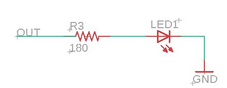
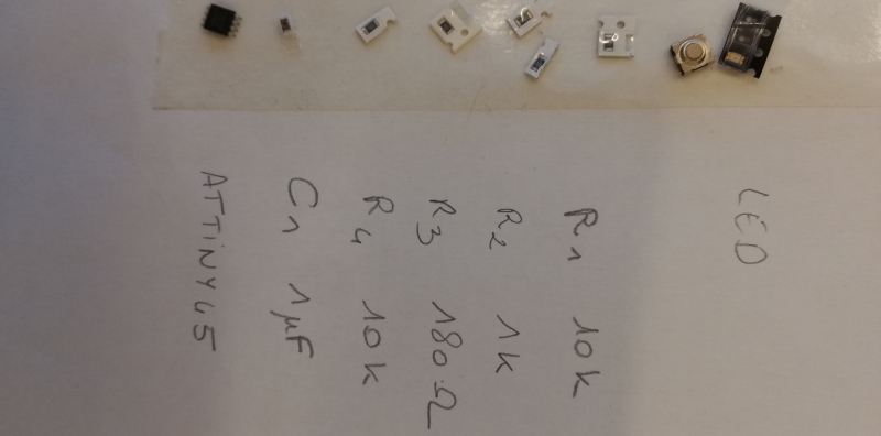
individual assignment : redraw an echo hello-world board, add (at least) a button and LED (with current-limiting resistor) check the design rules, make it, and test that it can communicate
Board drawing with Eagle
Here is an example of a board on which we have to add a LED and a button.
 |
 |
|---|---|
| Example for the hello-board. | |
 |
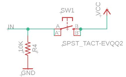 |
| Principle for LED connexion on a 5V board. | Principle for BUTTON connexion |
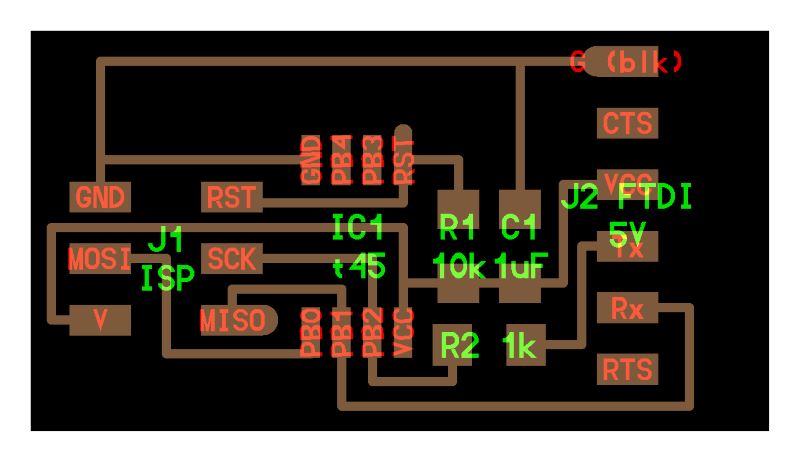
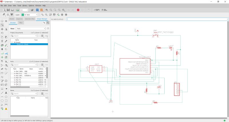
Schematic design
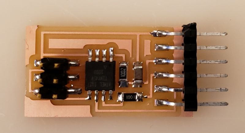
I use Eagle to redraw an hello-word board customized with an ATtiny45.
 |
|---|
| First schematic for the hello-word board. |
 |
| First board for the hello-word board using auto routing. |
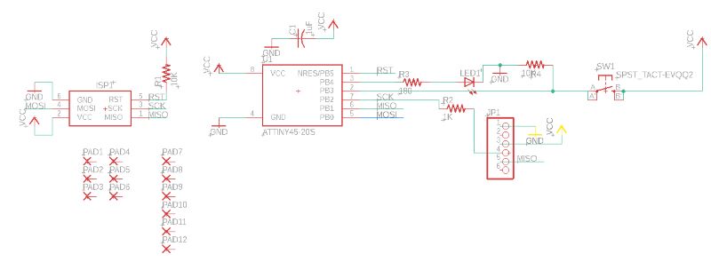 |
|---|
| Schematic simplified. |
Functions I use to draw schematic :
I use  to place new components founded into libraries.
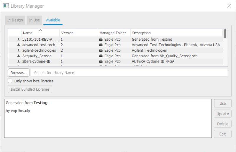
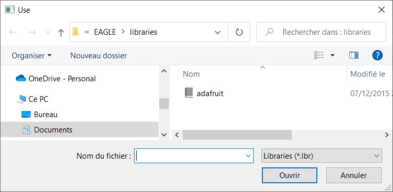
To manage libraries click on Library > Open library manager. Here you can add some libraries downloaded on Internet. I add adafruit, _hhn_attiny25_45_85 and SparkFun-Eagle-Libraries-main libraries.
to place new components founded into libraries.
To manage libraries click on Library > Open library manager. Here you can add some libraries downloaded on Internet. I add adafruit, _hhn_attiny25_45_85 and SparkFun-Eagle-Libraries-main libraries.
 |
|---|
| Eagle library manager. |
 |
| Adafruit library. |
You can copy  components and delete them
  .
.
I use  and
and  to move and rotate components. It’s possible to rotate components using moving button and right click.
I use  to add text like the name of the board and indications like VCC which can help for recognize connexions.
With  you can add components values and with
  you can name nets. When two nets have the same name the application propose to merge them like here :
(add photo)
You can control that all the net with same name are connected by using
you can name nets. When two nets have the same name the application propose to merge them like here :
(add photo)
You can control that all the net with same name are connected by using  .
.
With  you can connect components together and use
  to make junctions between nets.
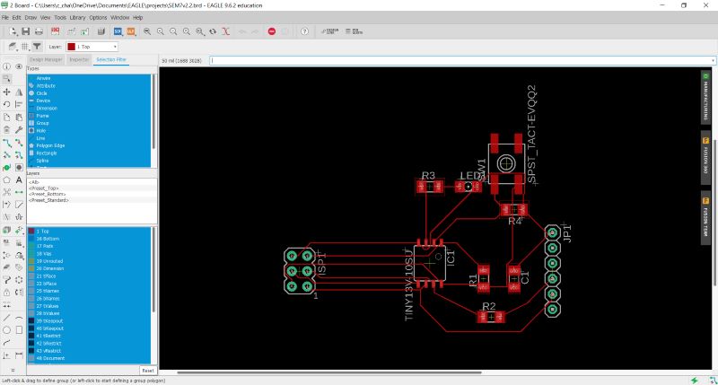
Board design
After doing schematic, you can designed the board associated with  .
.
(add GIF)
You can check your connexions with . It highlights all the net connected to the point you select.
With  you can make a polygon around your board to have a ground plate by naming it GND and using
  .
.
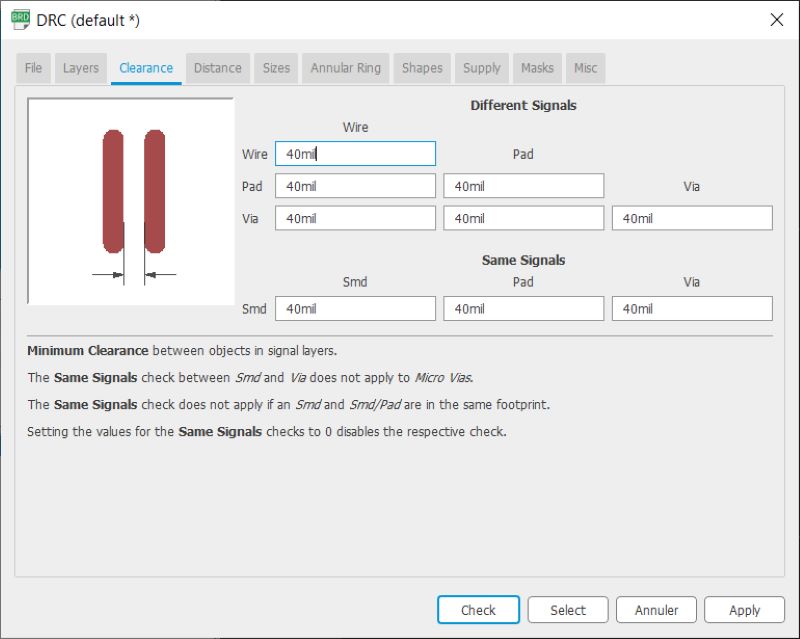
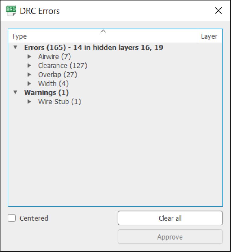
You have to register your design rules using DRC button and check your design.
 |
 |
|---|---|
| Design rules depend the process you use to mill or cut your board. |
This time I use manual routing with  . It convert connection you have done on the schematic by a real route. This button
  can be used to do an automatic routing.
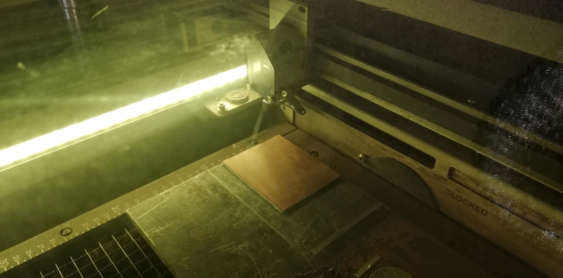
Board production
Before exporting your file you have to turn off some layers with  .
.
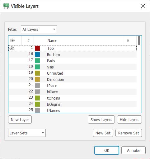 |
|---|
| You choose layers you want to engrave. |
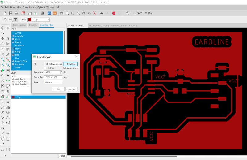 |
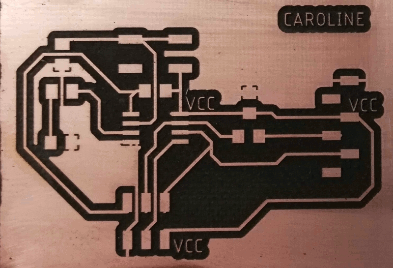
| Export the board as a monochrome image with 1200 resolution. Only the top layer is selected. |
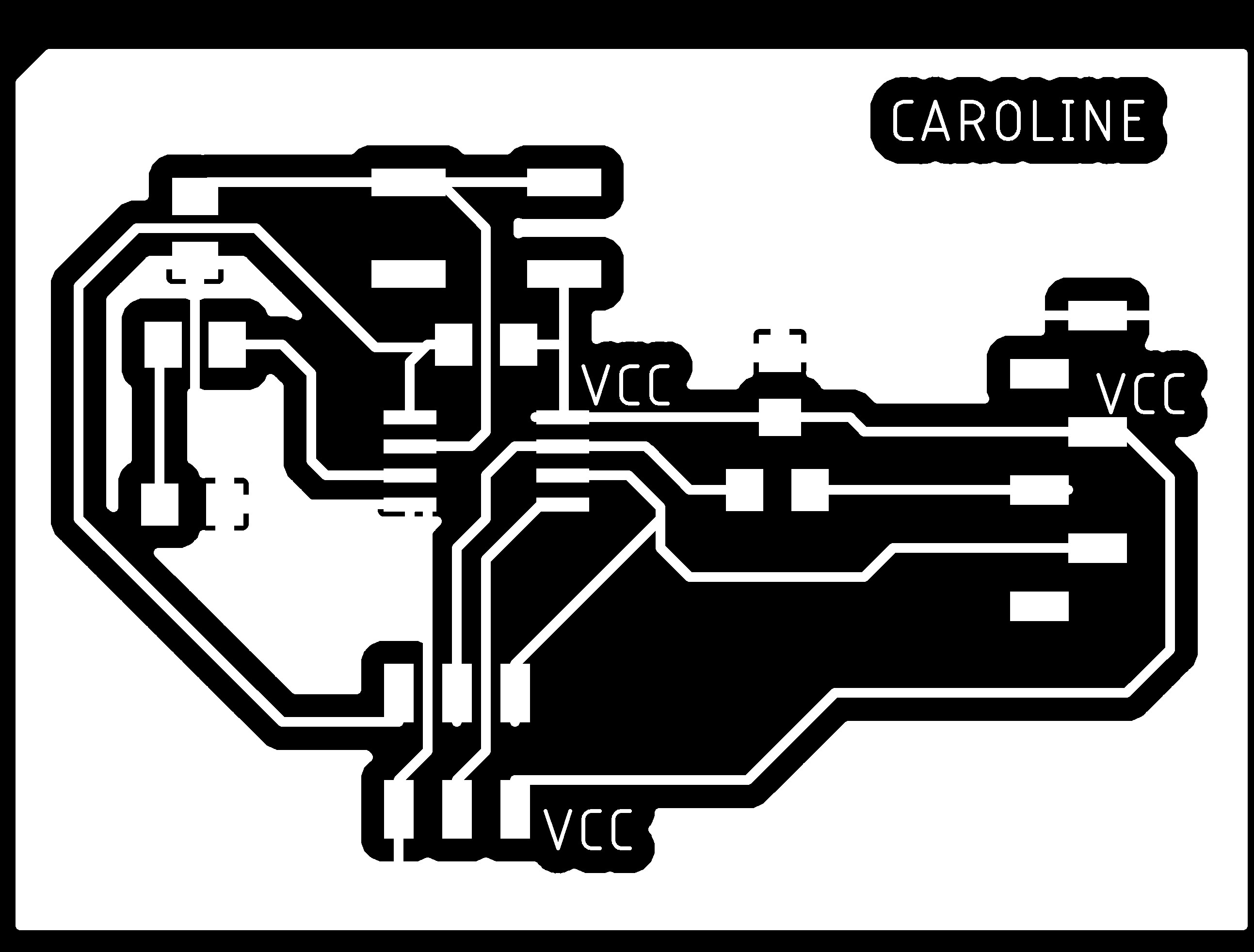 |
| File ready to be cut with laser. |
 |
| Vidéo ? |
 |
|---|
 |
 |
| GIF avec les deux images précédentes |
Observation of a microcontroller operation 
Analogic 
 |
|---|
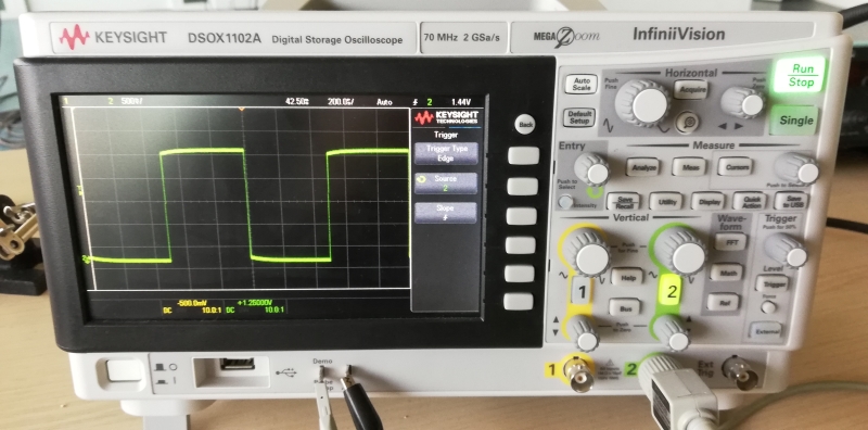
| Oscilloscope. Signal test sent by the oscilloscope itself to adjust settings. |
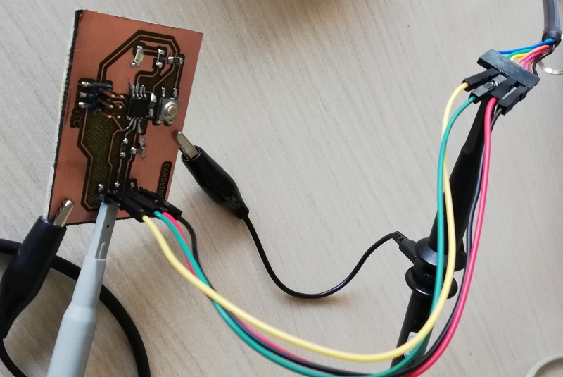 |
| Two sensors positioned on the board. Two black clamps connected to the ground. |
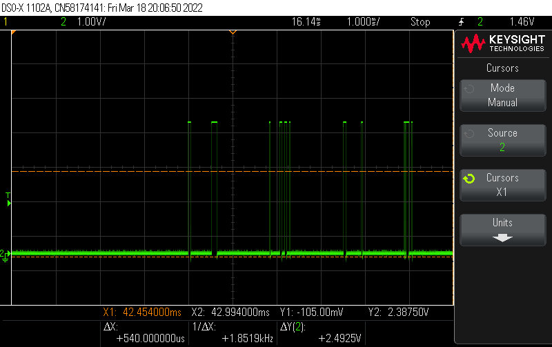 |
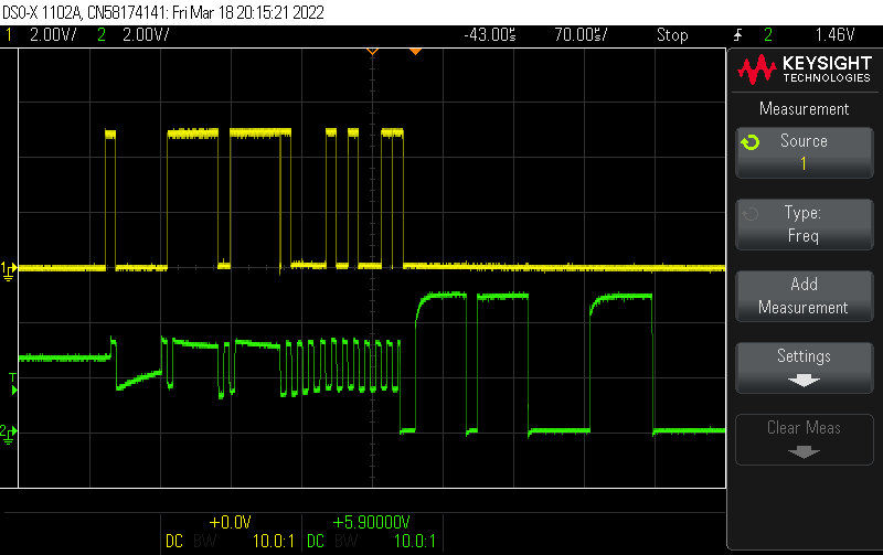
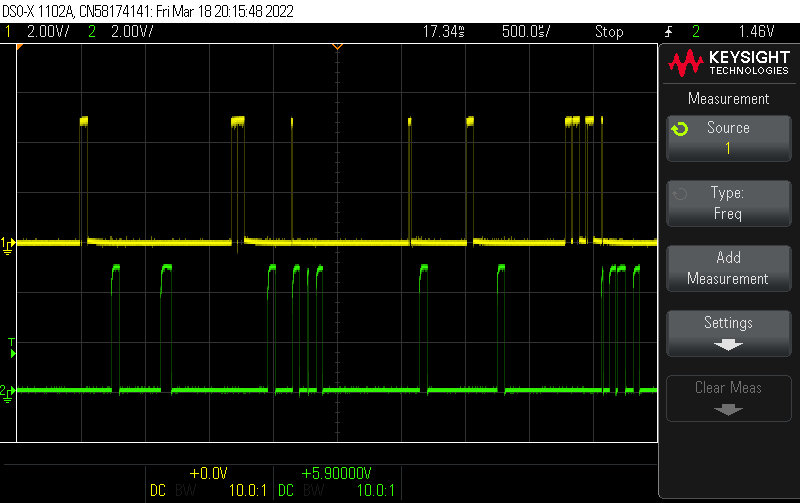
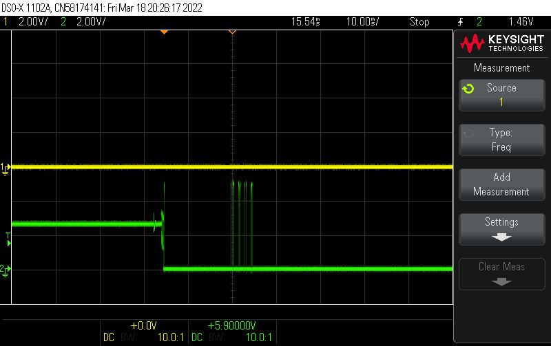
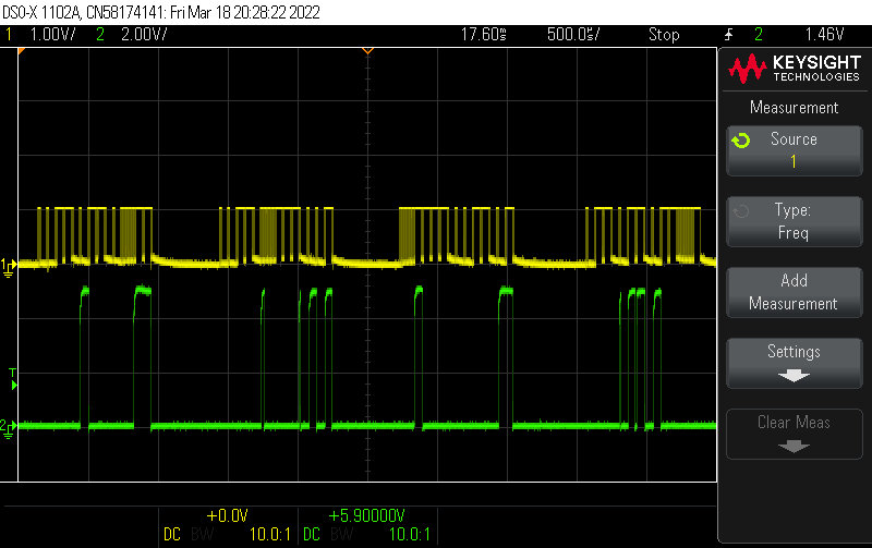
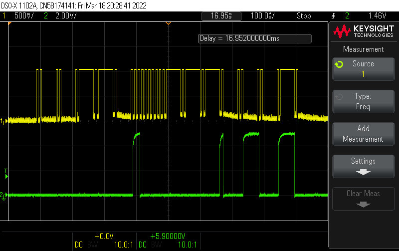
|---|
| MISO signal observed after sending an order to the card (programed with hello word) with computer. |
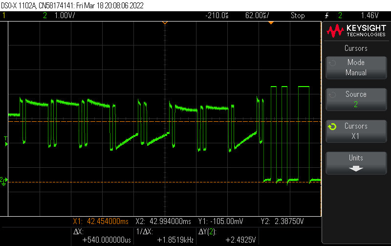 |
| MISO signal observed after sending an order to the card (programed with hello word) with computer (other part of the signal observed). |
 |
 |
 |
 |
 |
 |
 |
 |
 |
 |
Digital 
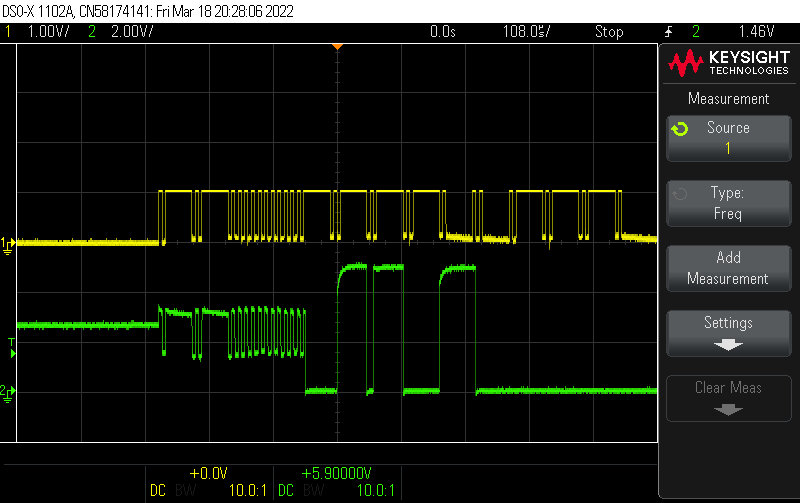
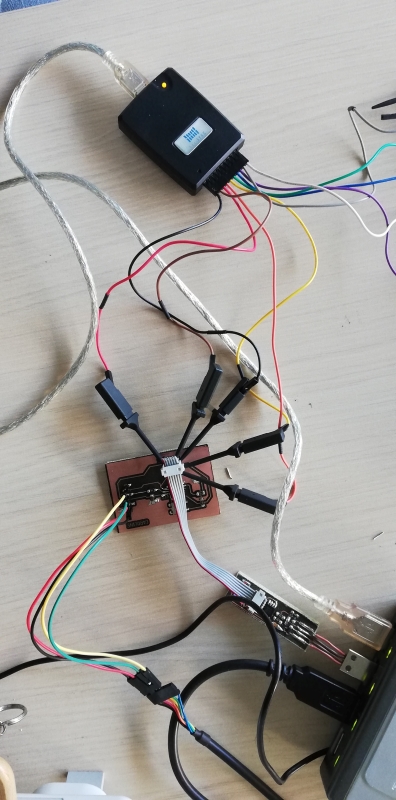
We use digital sensor connected to computer to observe digital response of the micro controller.
 |
|---|
| Digital sensors connected to the board. |
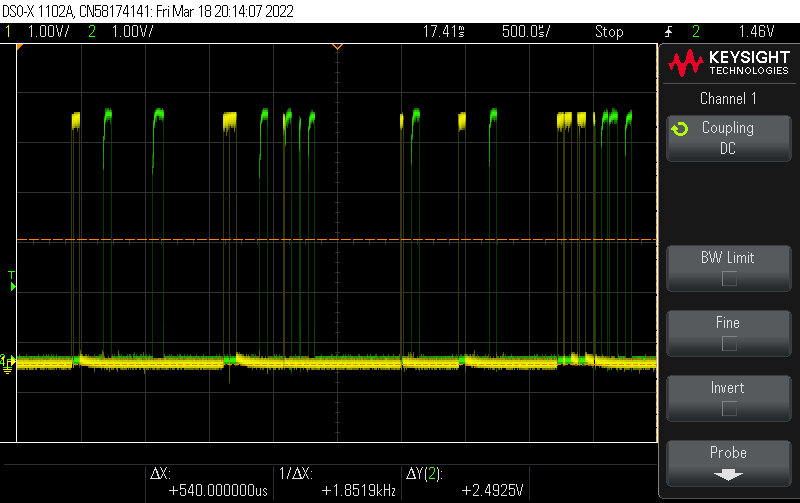
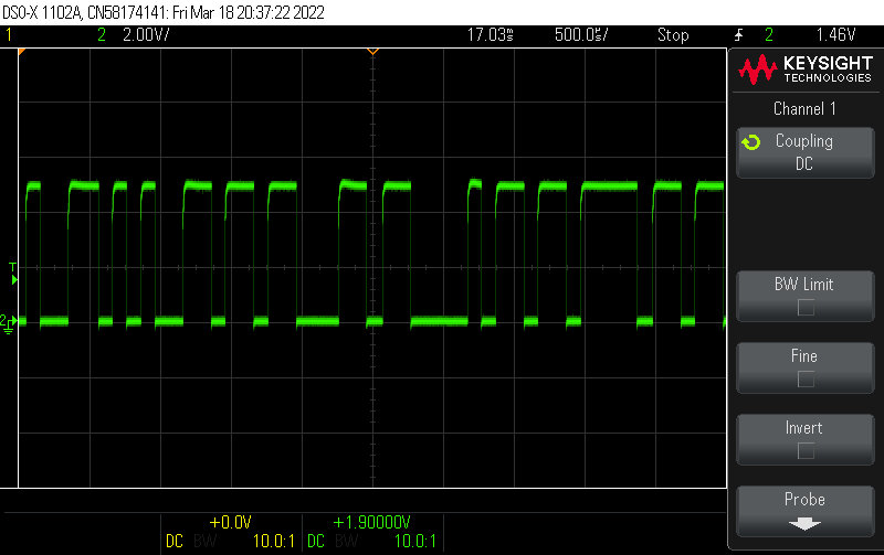
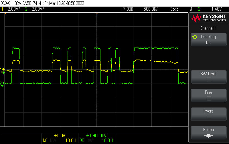
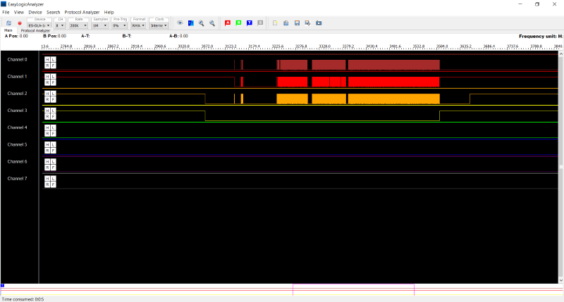 |
| Digital signal observed after sending my program for button and led. MOSI on channel O (red), MISO on channel 1 (orange), SCK on channel 2 (yellow), and CS on channel 3 (green). |
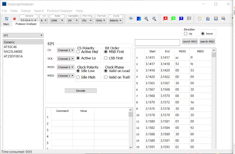 |
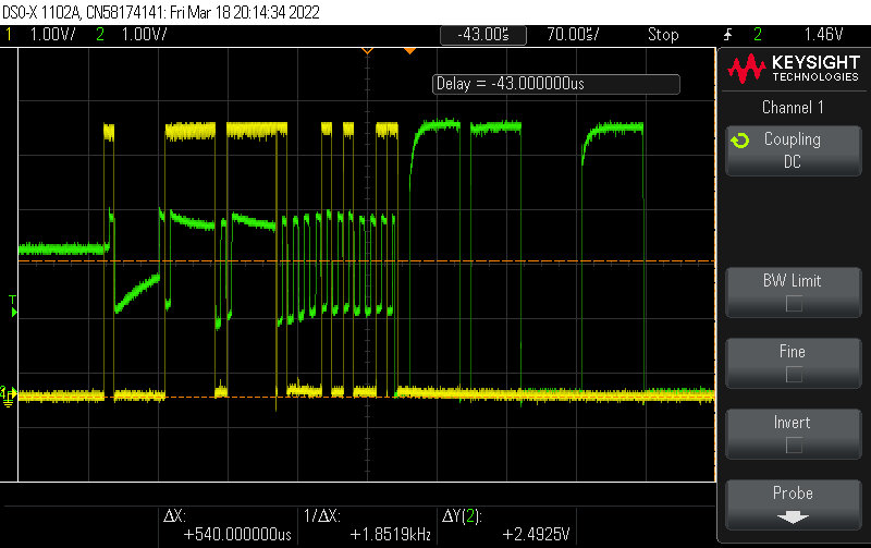
| Translation by EasyLogicAnalyser. Signal received by sensors MOSI and MISO. |
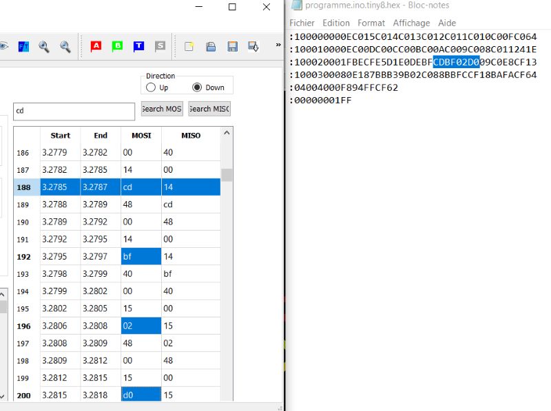 |
| Correspondence between code sent on the right (C) and signal read by EasyLogicAnalyser on MOSI channel. |