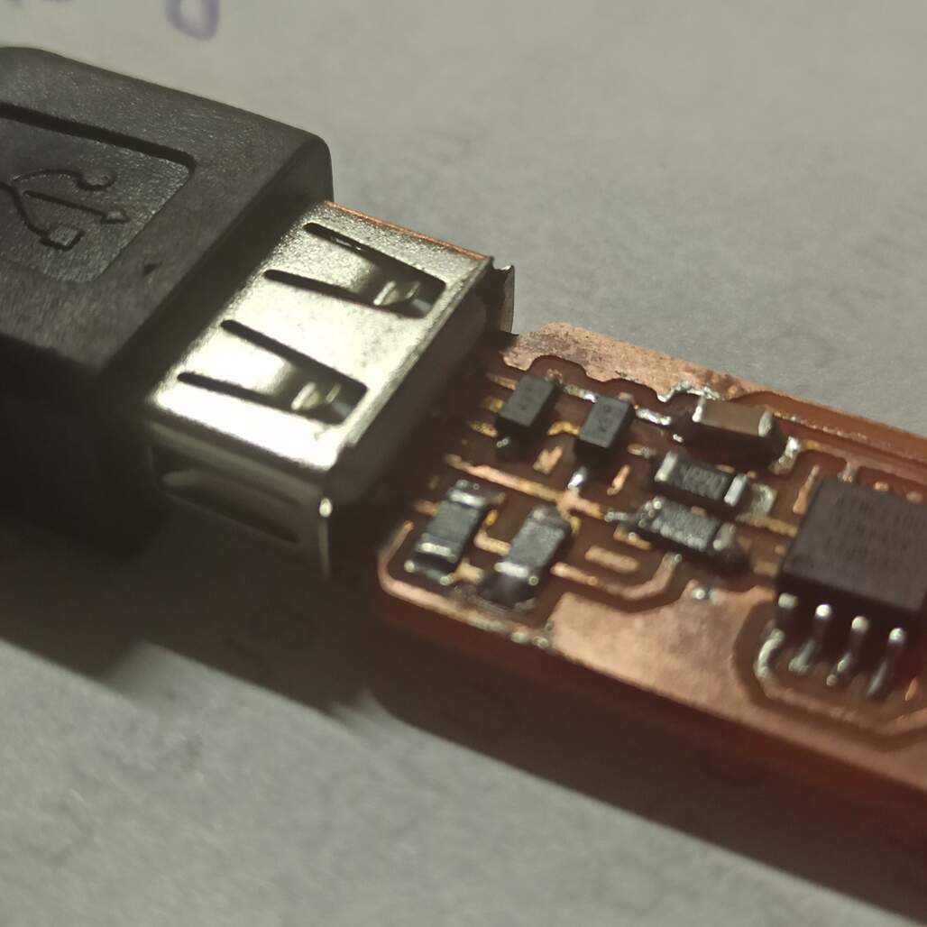
Programming the FabTinyISP board
As I was at home with another FabTiny board to program the ATtiny45 on my board I try to use an Arduino UNO as ISP to get the .hex file on the ATtiny45 using the next pin-out.
| ISP pins |
pin |
Led indicators |
pin |
| reset |
10 |
Heartbeat Led |
9 |
| MOSI |
11 |
Error Led |
8 |
| Miso |
12 |
Programming Led |
7 |
| SCK |
13 |
|
|
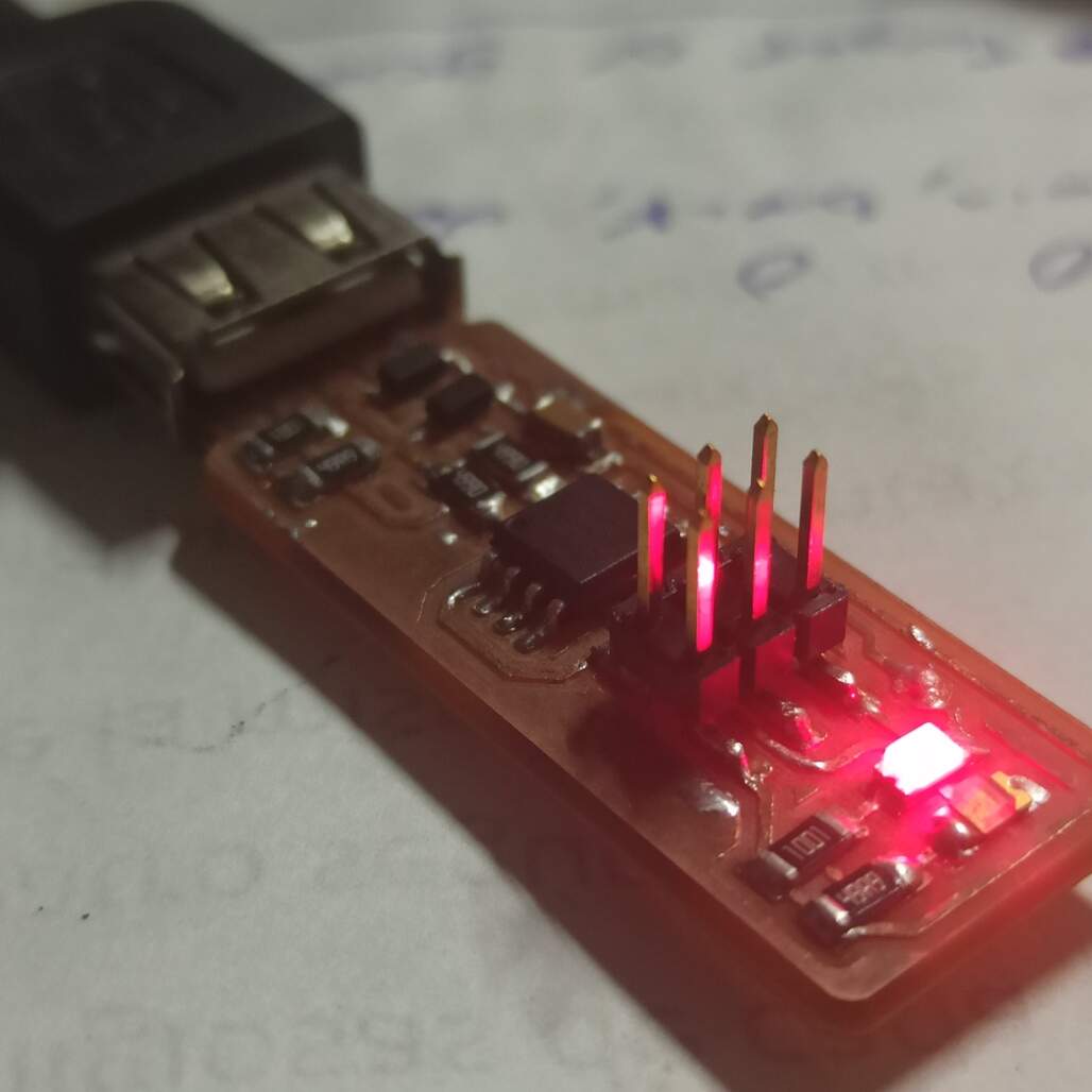
You also have to connect the VCC and ground to power up the ATtiny45, after that was connected by jumper wires, the LED's are completely optional but as it was my first time programming an ATtiny45 they help me to have more confidence.
I started installing software on my computer following the steps mentioned in this useful page about Programing the FabTinyISP. Also this page helps me to solve some issues that I step across when I was installing the needed software.
The programs needed in order to program the ATtiny45 are:
In the documentation of the FabTinyISP, they recommend the following steps to successfully program the ATtiny45 using the Makefile. And the programs installed previously via any terminal or bash that should be placed where the make file is located using cd.
make -> make flash -> make fuses -> test usb functionality -> make rstdisbl
Commands/Steps breakdown
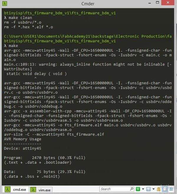
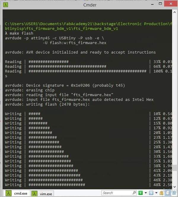
- make This command executes the first part of the make file and will also compile the program to a .hex file that contains the instructions for the microprocessor.
- make flash This will use avrdude to erase the memory of the ATtiny45, and load the .hex file with the compiled program.
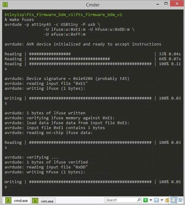
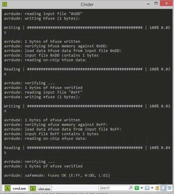
- make fuses This sets the fuses (bits that act as switches to configure modes and features as pinout and clock signal) of the ATtiny45, this first change to the fuses ensures that everything needed for the USB communication is set up but won't disable the reset pin.
- test USB The main idea is to get a computer to recognize the FabTinyISP as a valid USB, more info can be found here.
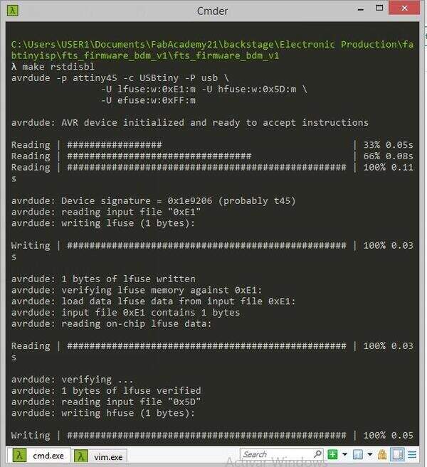
- make rstdisbl This is the last command that will set all the previous fuses + one that disables the reset pin and crate one more GIPO pin (output), and disable the avrdude ability to reprogram the ATtiny45.
As I was using the Arduino Uno as ISP I have to adapt these steps to make them directly on the console.
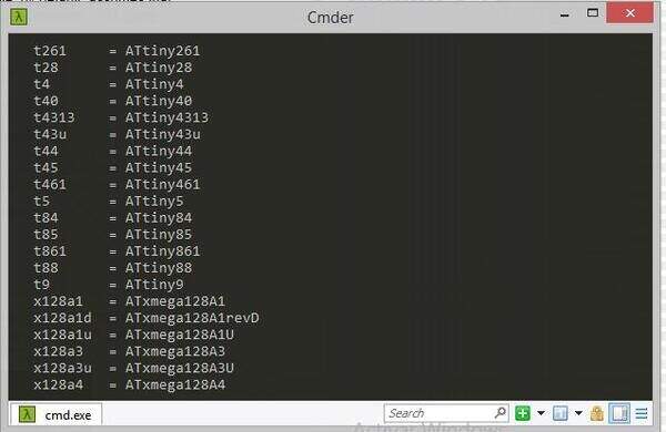
I started by displaying the list of possible target chips to be programed by avrdude using avrdude -p xyz to then choose the correct code and the set the flag -p t45 to select the ATtiny45 as the current target.
After that I make sure to know where the board was connected in this case COM4 so I set the next command to ensure that all the connections are properly made and avrdude is ready to program avrdude -c arduino -b 19200 -p t45 -P COM3 -n
Flag breakdown
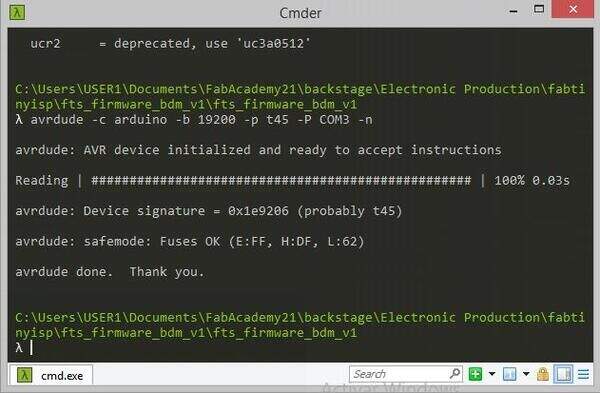
- -c is to define which programmer will be used.
- -b defines the baud rate of the serial communication with the programmer (especially needed for the Arduino)
- -p part number of the target microcontroller
- -P port on which the programmer is connected
- -n no write flag, here to make sure this line is only to test connections.
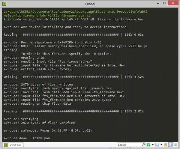
Using the previous command and changing the -n flag for a -U flash:w:file.hex, to load the .hex file to the MCU.
After that was done I try to test the USB functionally with no results because the fuses weren't set as needed for the USB protocol, so I then try to execute the make fuses without any success because the make file is not adapted to use the arduino as ISP. So there are not -b or -P flags, which default value works well for a USBTiny programmer but not for the Arduino.
Then I try to change the fuses manually but it didn't work because of the safe mode and how I did the command on avrdude. I decided to test and understand how to change one and then apply the knowledge to the other 2 fuses. but I choose the wrong one to test with, and I manage to write the fuse but it was the one that changes the clock signal. And after that, I wasn't able to reprogram the ATtiny45 because it needed an external clock or something like that and couldn't communicate with avrdude returning a 0x000000 as the chip signature.
After this I research and read about fuses and that help to understand how I ended up with the ATtiny45 'bricked' (a term used to describe an MCU that has a wrong fuse configuration), and also how to make a 'fuse doctor circuit' that uses 12v on the reset to force the fuses to the desired state, this was my first idea to solve the issue and reprogram my board. But Roberto suggests that I can replace the bricked ATtiny45 with a new one and try the programming again.
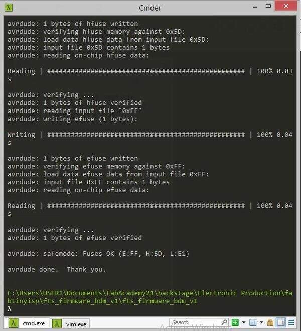
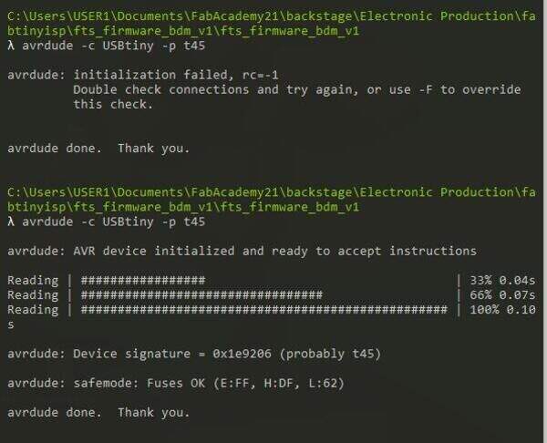
Once I remove the ATtiny45 and soldering a new one, using Camilo's FabTinyISP I finally manage to program the board and fuses using the Makefile and the steps described above.
And it finally works!
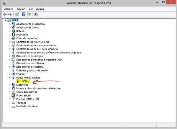
When connected to my my Windows computer it appears on the DeviceManager, and it actually can be used to program based on the ISP protocol