Week6; Designing Electronics
Week 6 is about designing circuitboards and learning the workflow in KiCAD or Fusion360-Eagle for that. In order to do so, some basic understanding of electronics is part of this week. If everything goes well I have a working Hello world board at the end of the week
Wednesday Global Class
Basic Electronics. I did learn a bit of electronic design in Delft, but that was a long time ago and only the very basics. So it was all very familiar but a great repetition for this course.
So Neil mentioned the different elements that we will use.
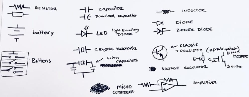 and he showed basically how they look and what they do.
Next to that he showed the workflow of KiCAD, which is at tool to design circuitboards with.
Weekly Assignment
Group assignment:
- Test the circuitboards and electronic elements with the tools in your FabLab Individual assignments:
- (re-)Design and fabricate an Hello World Board
- Test the Hello world board
Planning this week
Due to Corona, we have to split up the group in halves to work in the Waag, I am scheduled to be there on thursday (instruction and group assignment) and on monday and tuesday, the afternoons. I work on monday-morning, tuesday-morning and friday, so it is quite a tight schedule. I made my planning around this schedule.
| Day | Lesson | subject/activity | activities |
|---|---|---|---|
| Wednesday | global class | make this plan | |
| Thursday | local class explanation Electronics Design | Lesson KiCAD | group assignment measuring electronics |
| Friday | 'work' for my work | learn Fusion360 electronics | design Hello Board |
| Saturday | global open time | Make Hello Board | |
| Sunday | family-time | ||
| Monday | afternoon local Fab time | get my Hello Board milled | Soldering |
| Tuesday | afternoon local Fab time | Finish & test the board | Documentation |
| Wednesday | presentations | ready to present | fix last things |
Subject research
In order to follow along I went back in time and re-red my comics-book 'Resi and Transi'. It explains everything about analog electronics and although it's from the 80ies the resistor is still the same.
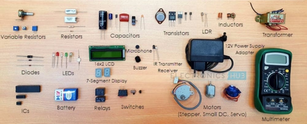
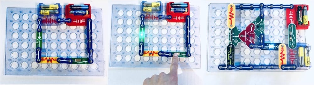
![]() And I played around with our electronics-set that we used with our children. All the basic elements are in there, and some nice integrated circuits. I had fun with basic electronics to get reminded again of all the different parts
And I played around with our electronics-set that we used with our children. All the basic elements are in there, and some nice integrated circuits. I had fun with basic electronics to get reminded again of all the different parts
Online I found the Electronicshub to be very useful for translating my Dutch knowledge in English and American component-names.
Thursday instruction
Henk explained about
- Basic circuits and how to calculate with them.
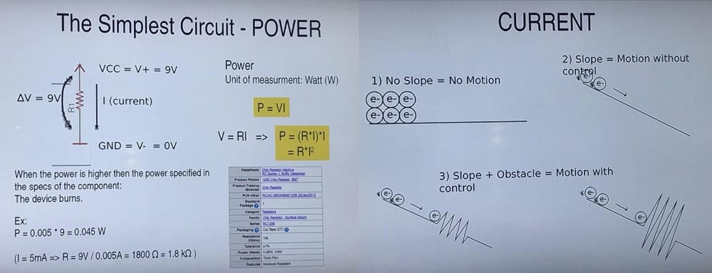
- Ohms law: R=V/I (Resitance equals Voltage divided by Ampere) and Current V = R*I (Voltage is Resistance times Ampere)
- Watts P=VI (and with V=RI P=RII)
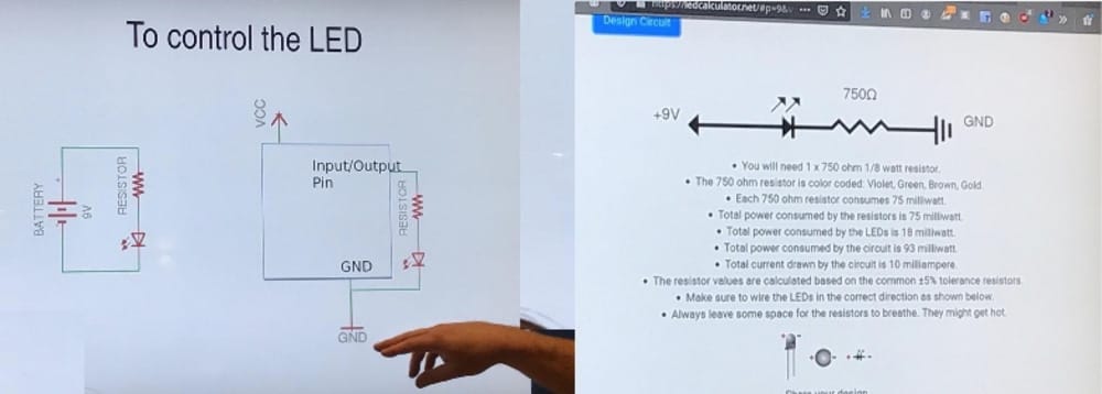
- LED's are non-ohmic (I like the word) and therefore they need a resistor in the circuit. (calculations at LEDcalculator.net)
- Circuitboards and the different views of them while designing.
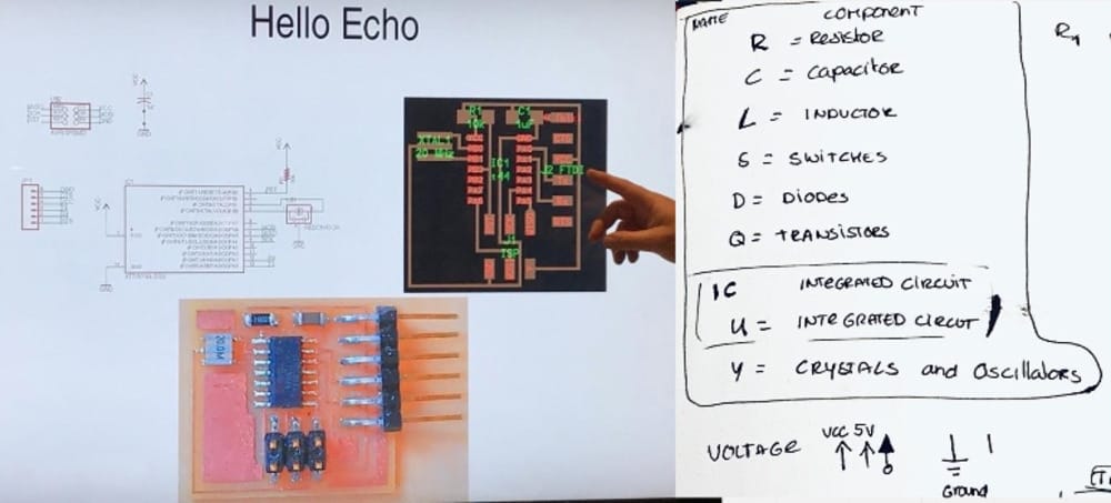
- The Letters that are the equivalent of the symbols for the different components.
- Parallel and series and how that works with resistors and with batteries.
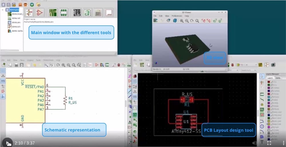
workflow in KiCAD/Illustrator/Gimp:
First use the schematic editor
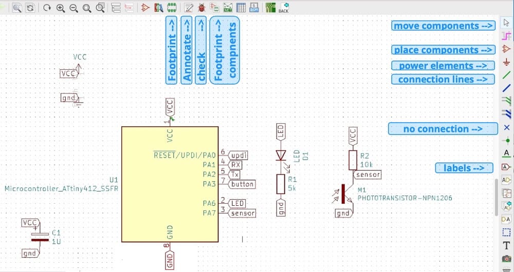
- Open the schematic editor
- Upload the right components.
- Arrange the components so that they are schematically fitting
- Connect the components with green lines or labels
- Check if everything is annotated
- Check the electronic system, fix all mistakes
- connect footprints to the components, Apply
- save the schematic and continue to the PCB-Layout-editor
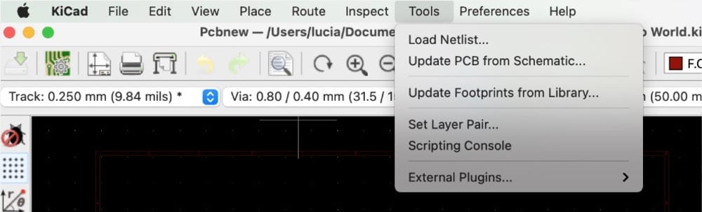
PCB layout editor
- First 'tools; update form schematic' and check if there are no errors.
- Place the very compact version of all the footprints, with white lines between all connecting parts.
- Spread the different footprints a little and turn and move the footprints so that the white lines are not crossing at all (or at least very little).
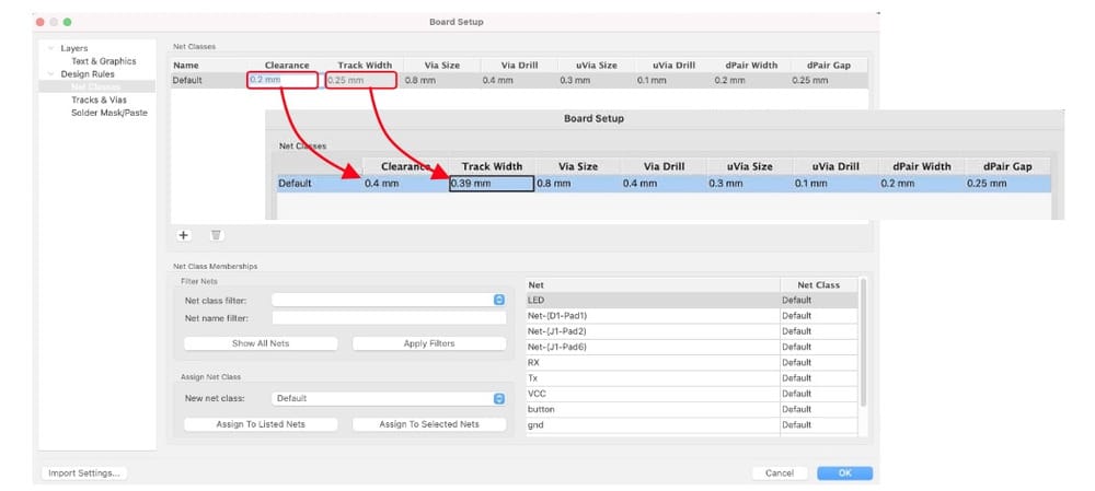
- Update design rules: settings for the trace-width and cut-width.
- Trace the board (green line-icon on the right)
- draw an outline
- export the copper-layer and edgecuts-layer to SVG
- print mode
- edge cuts
- one file per layer
- board area only
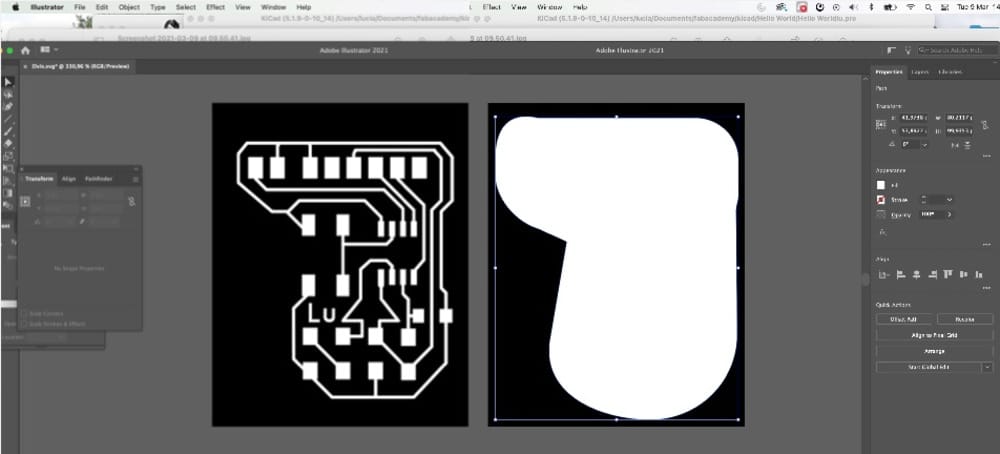
Illustrator/Photoshop/Gimp
- set measurements in mm
- Invert the board (black is milled away) (if you invert look at the line-thickness)
- set the dpi to 1000 dots per inch
- save the two different files (Traces and outline) as .PNG.
Group assignment
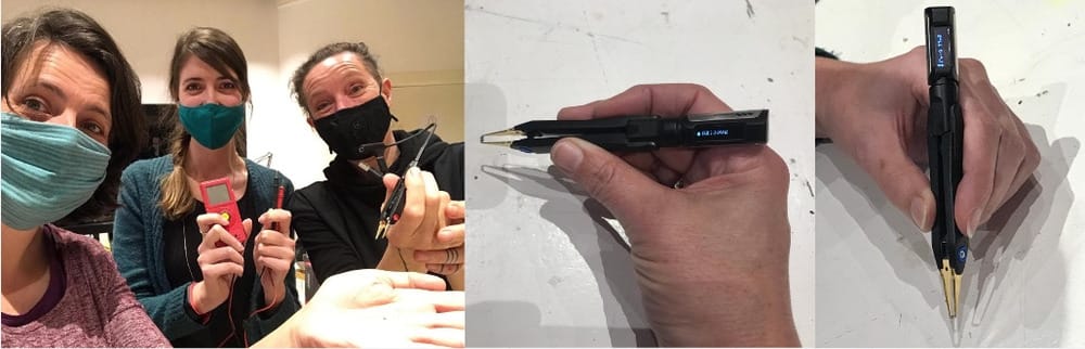
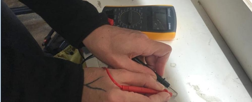
For the group assignment we had to look at the different measurement-tools and play around with them.
oscilloscope
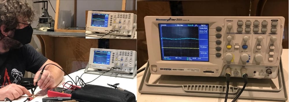 the oscilloscope gives an overview of the current during time.
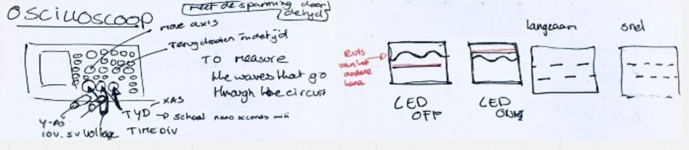 It is also possible to record a while in order to zoom in. Playing around with the time and voltage level can zoom in on really fast electric differences

Logic analyser
a logic analyser can evesdrop what is happening in the circuit. You can so to say see the bits passing by.
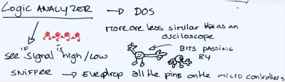 On the laptop you can read what the logic analyser shows. for example with the program pulseview.
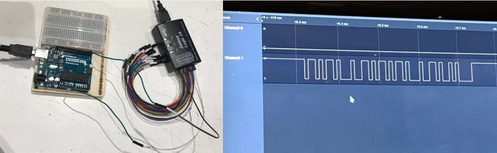
We (Loes, Nadieh and I) played around and especially the 'magic-tweezers' were fun to analyse odd components with.
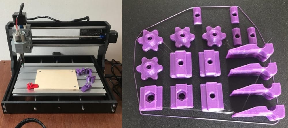
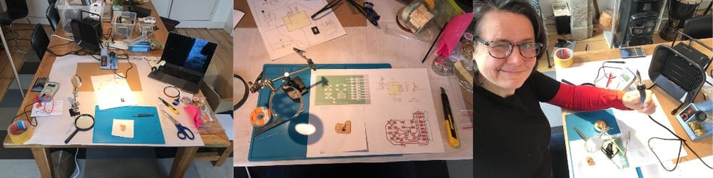
Milling machine at home
On friday, we did not have the assignment yet and I planned to work on FabAcademy in the morning, so this was a great time to assemble my 3018-pcb-mill.
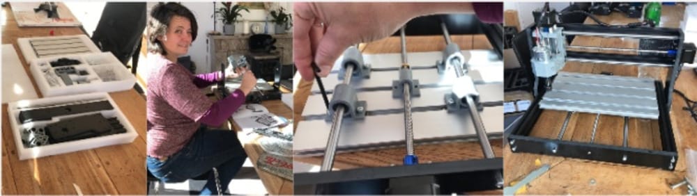 It is quite a basic setup, and after assemebly I played around with the 3d-printer I assembled earlier this week to make clamps from Thingyverse. And I redesigned one of the nut-holders so I could make a flat wooden bed so I can tape my boards on them. Good fun, but took me the whole day ;-) I did not mill yet, because I don't have the right milling-bits yet. I did go to the local electronics-shop and they will help me out, they bought the inventory of a pcb-milling-factory so next week they will have a whole lot of millingbits for me. And since we are in lockdown it is very cool that finally we can visit shops again.
Individual assignments
Design and produce a Hello world board
this is what we got for the assignment:
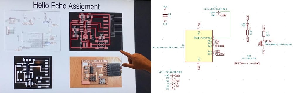
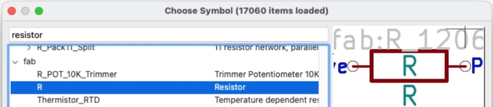
I tried to follow my notes and worked it out in KiCAD. It did not work, the notes from thursdays quick tour did not give me all the information needed to tackle this baby.
S0 I looked online and found a nice workflow with images of the right buttons for the different steps.
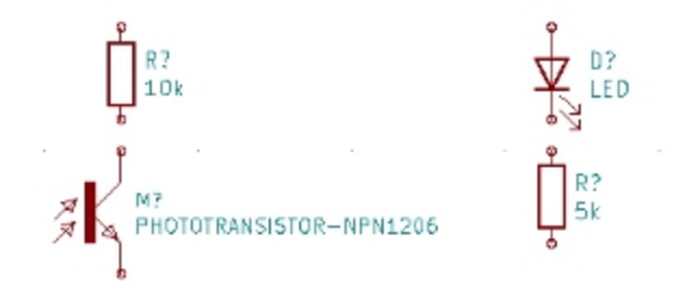
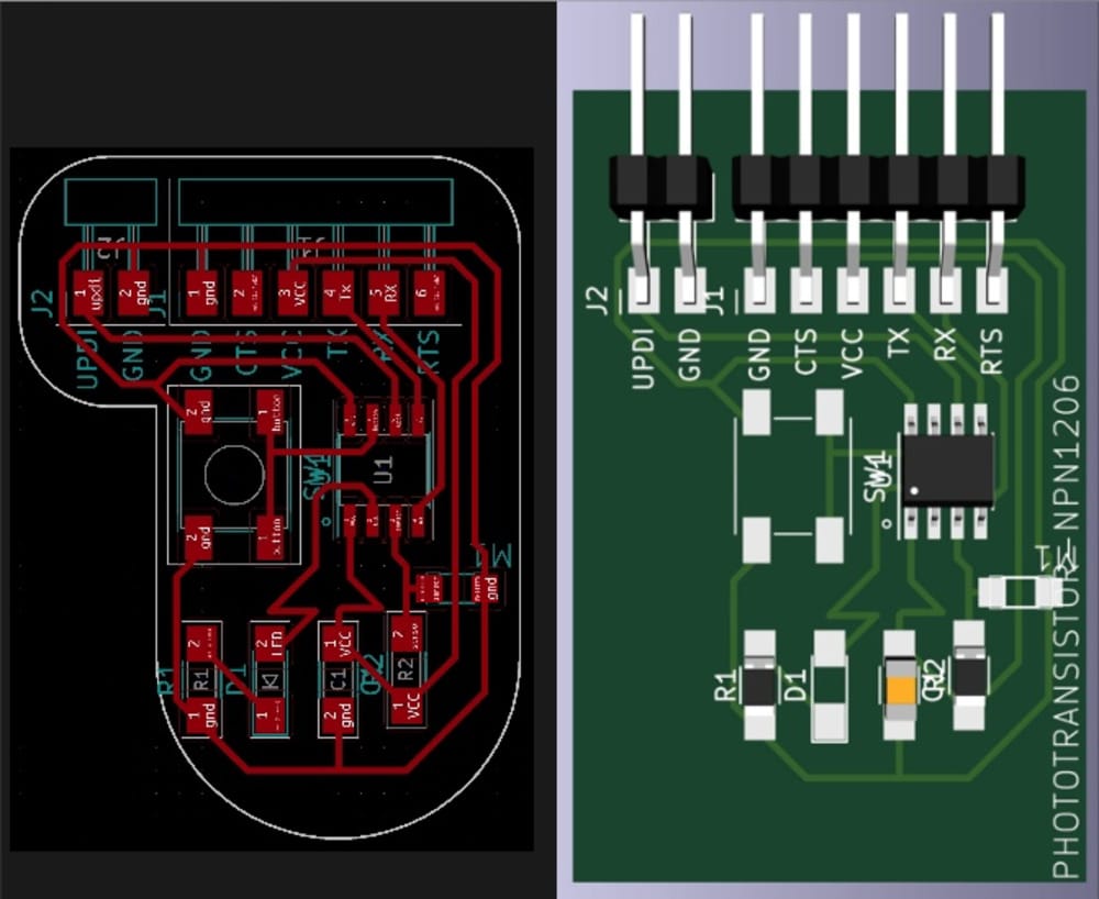
I made the schematic design but when I tested it I had quite some errors though:
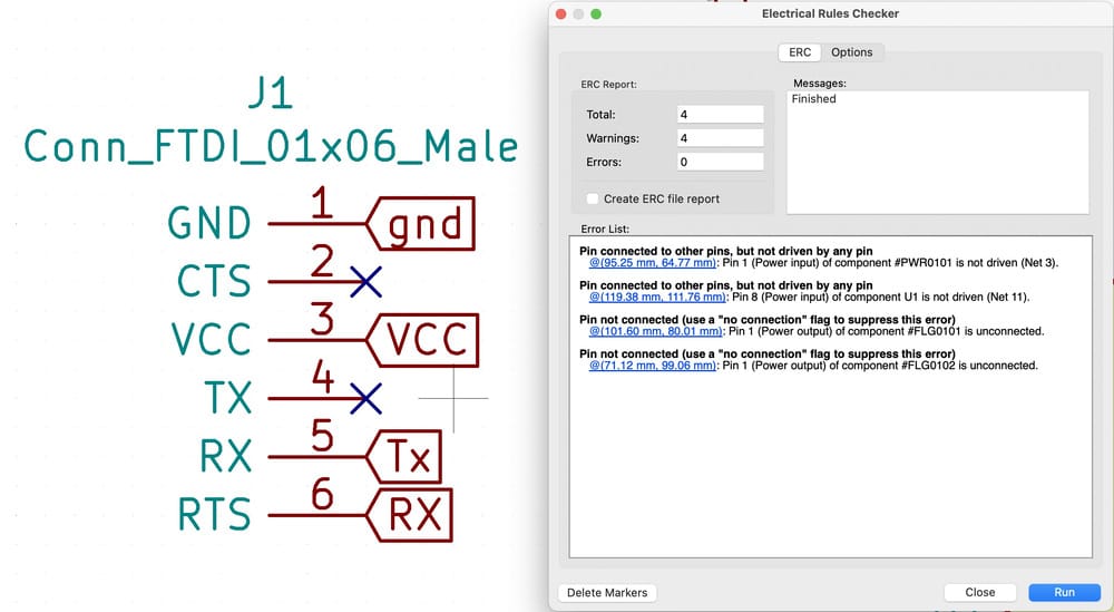
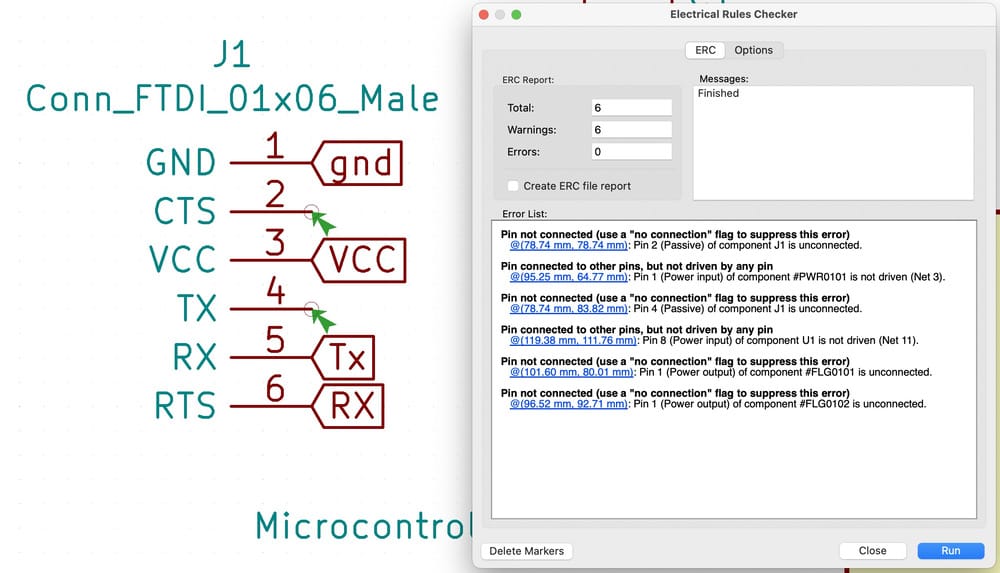 I looked into 'no connections' and found how to fix that. the 'power-mistakes' I could not fix by myself.
 But luckily the guys at open-time on saturday helped me out: saying that they found online that I need 'power-flags'. More importantly: They assured me that such a mistake is not really stopping the process, you can still make the .PNG and the board 'won't know' that it had initially no powerflags.
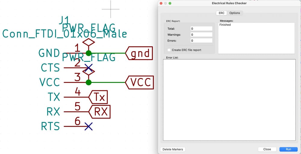
I looked into powerflags in kiCAD, but could not find them anywhere. I thought it would be labels, but they were not there. So I just went on making the board. Only on monday, when Nadieh had fixed the same problem I found the powerflags (under 'power') and added them to my board. No Errors anymore. yessss
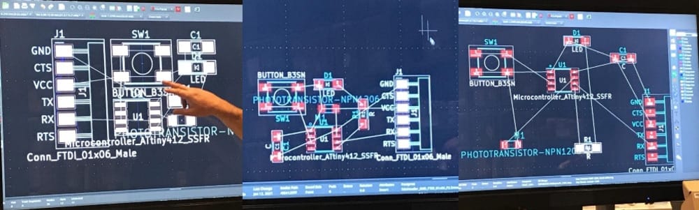
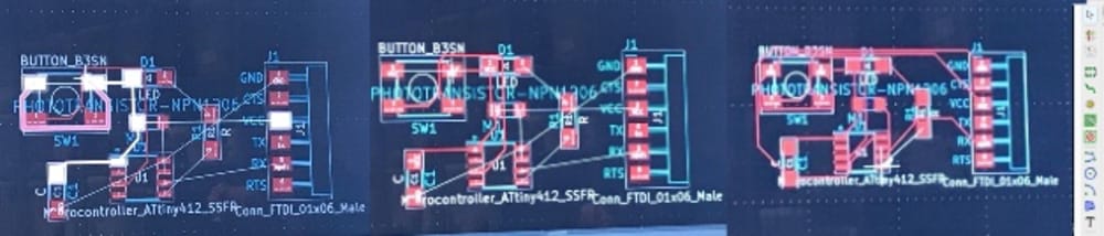
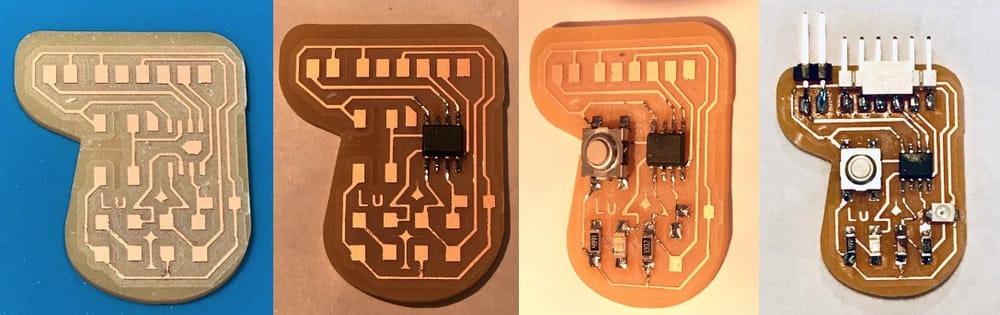
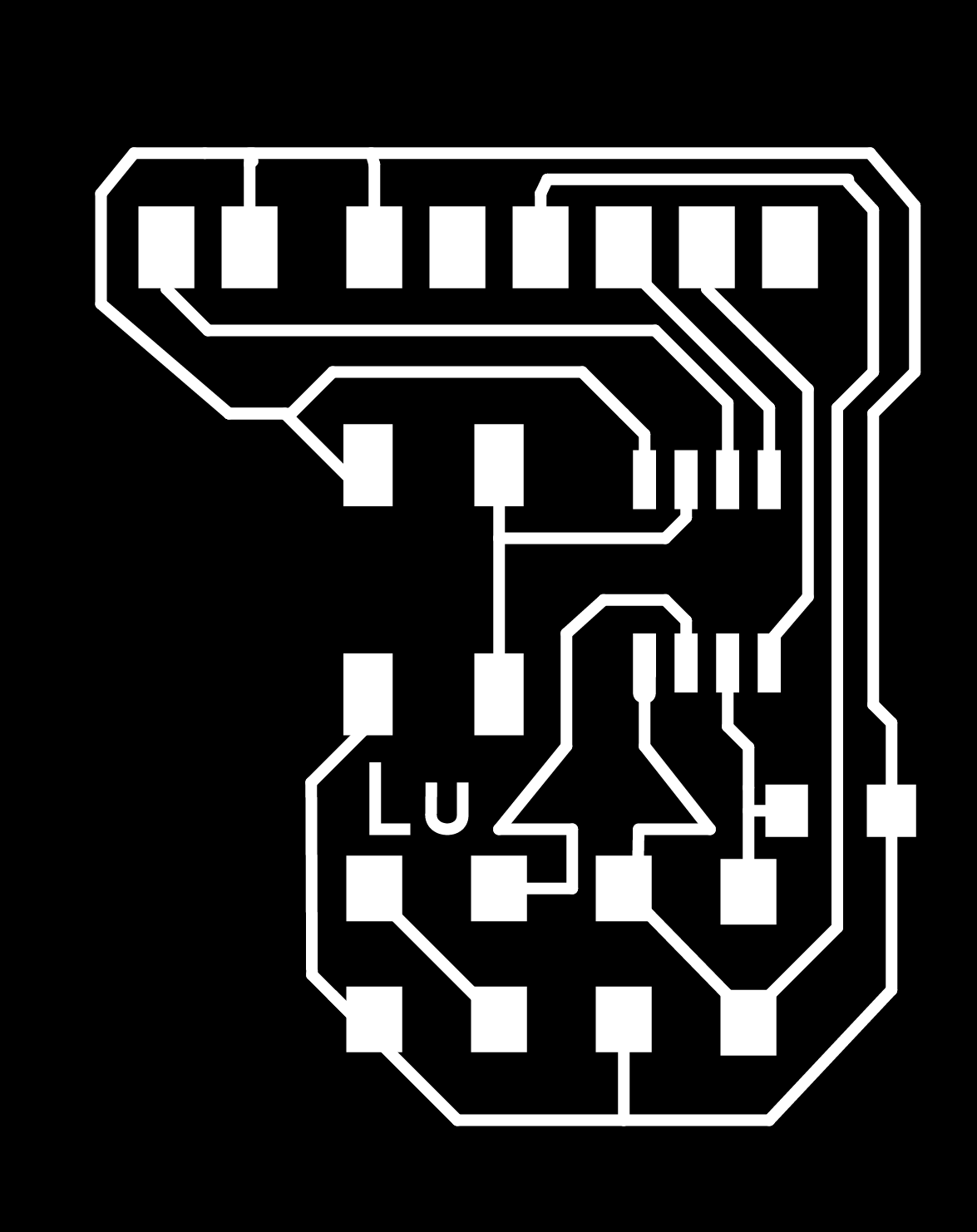
first board
I played around with the tracing and found it easy to have the 3D view next to it, so I could see the direction of the pins.
Also I wanted as little bridges as possible, because that would make soldering easier..
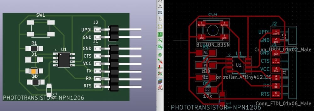
Now for the looks.
I had some fun playing around with the components and thought it could maybe be a boat or a rocket, but then I clearly saw Elvis (he lives) and decided to change some components around to give Elvis the real hairdo. (with sticking out pins, hahaha) I played with the outline and gave him a nose.
Monday Waag-time.
Our milling-machine is not a quick-boy so I had to wait until 5PM before I could start milling. I made several versions of the .PNGs and when I put them in mods it would not naturally grab everything.
Milling
First I taped a new board on the sacrificial board. (the previous board did not have place for my elvis) The Roland was milling happily away and then, at the end it decided to mill the air instead of the board. Henk did not have time to have a look and the computer seemed stuck on mods (all red lines around the boxes)
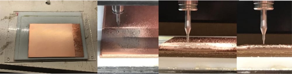
So I had to start again, it could barely be done before closing-time, but it worked. (i forgot to speed up the milling for the outline and that made it really slow.)
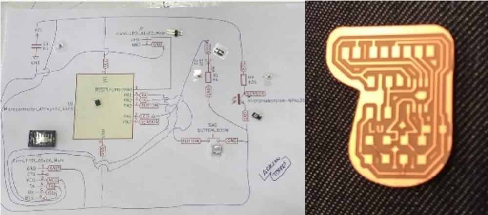
Mean while I did the orderpicking for the components and taped them to my first schematic drawing. That way I could do the soldering at home. I packed everything and with my freshly milled board I went to the train. It looked great.
On tuesdaymorning Philip said that the bit was broken and I told him that it worked fine for me on monday, but on wednesday Henk looked closely at the pictures I made and said that indeed the milling-bit was broken. (see most right picture) So my board broke it quite tidy, because my second try on monday with the same mill-bit it did work out quite nicely.
Tuesday at home
I got to use my home set-up for the electronics. It was great unboxing all the different parts and putting everything on the dinnertable.
the different stages of the board. It took some time to figure out what the polarity of the photosensor was, so that was the last component I soldered.
Measuring it went fine, it was quite easy and clean soldering.
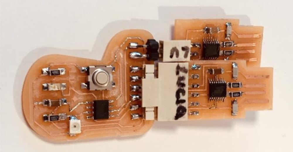
Henk told us that this was the end of the assignment, but on tuesdaynight he realized that we did have to test and program the board. Sadly enough there is no time to figure that out.
Of course due to the elvis-hair the two connectors are next to each other (FTPI and UPDI). I already made some plans how I can move the UPDI-plug a bit around or I can make an extra cord to connect it, but first test... and it does fit.
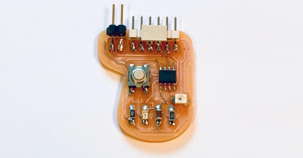
the result
here is my Elvis with sticky hair.
Links to Design-files
here are the links to the designfiles of this week: