Week 4; Workflow making an ISP, UPDI, JTAG
This week the workflow for milling and soldering a circuitboard is explored. we learn how to use the small cnc-milling machine and with that mill a circuitboard. And we'll collect all the parts and solder them to the board. after that it is time to test and debug
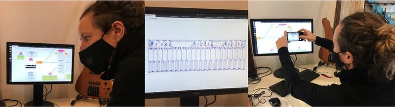
Wednesday Neil's Class
Neil explained about the CNC-setup, the drills, the way how to sent an design to the millingmachine. Other options to make circuitboard and the basics of soldering.
Weekly Assignment
In my own words
This week we have two assignments:
- A group assignment to learn about the small cnc-milling-machine to make boards ending up with a testboard with the specific measurements that our Roland can mill.
- An individual assignment to make a working board. Either UPDI, FTDI or JTAG. So to learn the workflow of milling, soldering and debugging the electronics.
Planning this week
Due to Corona, we have to split up the group in halfs to work in the Waag, I am scheduled to be there on thursday (instruction and group assignment) and on monday and tuesday, the afternoons. I made my planning around this schedule.
| Day | Lesson | subject/activity | activities |
|---|---|---|---|
| Wednesday | global class | make this plan | online research on electronic parts |
| Thursday | local class explanation of the CNC-machine | group assignment CNC-setup | printing my own first board |
| Friday | 'work' for my work | Documentation | |
| Saturday | global open time | any questions? | |
| Sunday | - | - | family-time |
| Monday | afternoon local Fab time | get the board soldered | and debugging |
| Tuesday | afternoon local Fab time | fix everything what is needed. | Documentation |
| Wednesday | presentations | ready to present | fix last things |
ISP, UPDI, JTAG Online research
these are the things we will solder this week. What are they?
ISP
ISP stands for In-System-Programmer. It is a small circuitboard that is used to program a chip that is already fixed to a circuitboard-system. They were invented to make the workflow easier for a factory so you can first make the system and then program the chip. (before that, factories would buy already programmed chips.) When re-writable (E)EProms were invented, the ISP became the standard to re-program the chips. On a Arduino the ISP is also on the board. But with the Fab-academy we will make a separate ISP so we can program several boards with it.
FTDI and UPDI
These are used for programming and communication with the microcontroller FTDI is a communicationprotocol for serial communication, widely used and still very popular. UPDI is used for the newer generation ATtiny's and uses only 2 pins via USB serial communication.
JTAG
JTAG stands for Joint Test Action Group. JTAG was needed in the 80's when the parts on a circuitboard became so small that it was impossible to test them separately. With the JTAG standard it is possible to debug, program and test the components on a board with a 5-pin connection. Through this connection the board and chipconnections and the internal electronics can be tested by stimulation and receiving echo's from the board. this testing is called debugging. SAM D processors are programmed with a JTAG programmer.
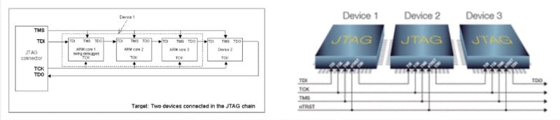 There is also a reduced pin count JTAG with only 2 pins.
- TMSC (test serial data)
- TCKC (test clock)
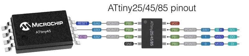
ATtiny or TinyAVR
ATtiny is a family of microcontrollers with a limited amount of pins.
ATtiny45 and ATtiny85 are models that are used in the things we will build this week.
Learning activities
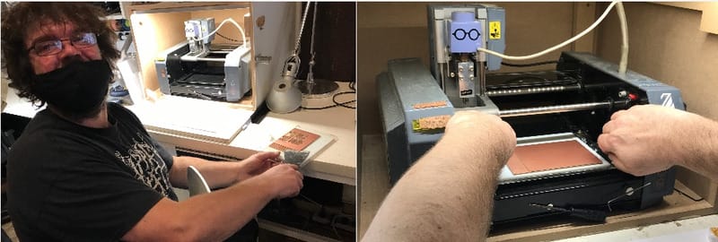
Local class, machine explanation and group assignement
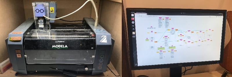
Thursday I was at Waag and Henk explained everything about the possible boards to make this week and how to mill them with the cnc-drilling-machine. At waag there is a Roland Modela MX20, small position millingmachine. The accuracy of the machine is 0.002 mm. the drills are much bigger, we will use a 0.4 mm millingbit for milling the traces and a 0.8 mm millingbit to cut out the board. The X-axis an Y axis are given by the image you put in, the Z axis is given by the height of the millingbit.
MODS setup
- Open Terminal and use
MODSto open MODS - In MODS choose
ProgramsthenMXD mill; PCBthe millingmachine is on portdev/tty/usb0 - To get the right connection at first startup at the module 'Web Socket Serial' (nr7 in the picture): push the buttons
close the socketandclose the port, thenopen the socketandopen the port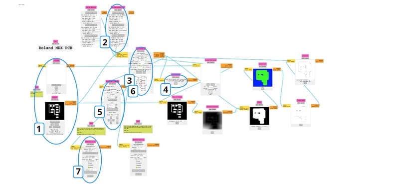
-
Let MODS read the SVG or PNG. For now we will have a PNG of the traces first. (the matching 'interior.PNG' will be used later)
- Check if the 'artwork' has a DPI between 500 and 1000, since the milling is very high accuracy.
-
In the block
setPCB defaults(mm)click the buttonMill tracesthis changes the settings in theMill raster 2Dblock to the default settings for milling the copper layer.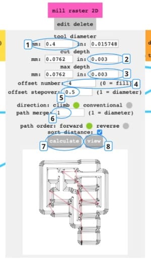
-
In the
Mill raster 2Dblock, some of the settings need to be adjusted:- At 1: Set the tooldiameter to 0.4 (It seems that it is almost right).
- At 2: set the cut depth to 0.003 inch.
- At 3: set the max depth to 0.003 inch.
- At 4: the standard amount is 4 offsets, if the whole boards needs to be clean set this to 0
- At 5: the stepover How far the paths are fnext to each other is relative to the bit-diameter. standard 0.5 diameter.
- Direction is standard to
climbwhich is the way the bit turns and with climb the chips are taken away from the front towards the undrilled side and the back.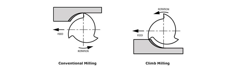
- At 6: the path merge, is relative to the bit-dameter.
- The path order is standard on
forward - At 7: Now push
calculateThe 2D milling lines will appear in the small viewer in the module. - At 8: For a better look push
viewand a bigger preview will open in another tab.
-
Check the 3D view in the module 'View toolpath'.
-
In the module Roland MDX /iModela set the cut speed to 1. This is very important, because the millingbits are very vulnerable and will break at higher speed.
Machine setup
Now move to the Modela machine. And do the set-up there.
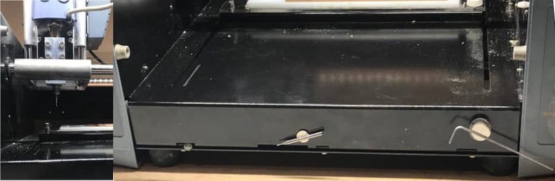
Installing the PCB-plate
First check if the right plate is still there (onesided, doublesided, enough space for your design...) If necessary change the plate:
- Remove the plate with a puttyknive (imageleft)
- Put doublesided tape nicely and straight on the board and cover most of the board so it will stick on as straight as possible and even small cutouts wil stay stable while milling.
- With the tape stick a new plate on the sacrificial board. Push down firmly so it is stuck and straight.
- Fix the board in place in the machine. Tighten the screws 'snug'.
Change the millingbit
The millingbit for the trace-milling has to be very small in order to get good detail and nice soldering-spots for all the components. downside is that they are very vulnerable and quite costly.
1 Turn on the machine. it will move to home at the right and the back.
2. Press viewto move the bed towards de back and the millingbit towards the left. In this position it is possible to unscrew the millingbit.
3. lower the millinghead so it is about 1,5 cm under the trolley, this way the screws are reachable and the millingbit can move out of the machine.
4. turn the millinghead so that the right screw (with a blue marker dot) is visible.
5. Make sure to hold the bit between your fingers so it won't fall and break.
6. Loosen the screw with the smallest alan-key (stuck on the magnet on the front of the machine).
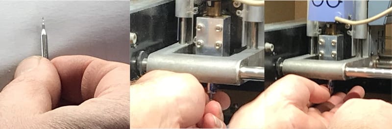 7. Pick the right millingbit from the box, on the side are the newest and towards the middle the oldest.
8. Hold it safely between two fingers and insert the bit in the millinghead. tighten the screw 'snug' and the change is done.
7. Pick the right millingbit from the box, on the side are the newest and towards the middle the oldest.
8. Hold it safely between two fingers and insert the bit in the millinghead. tighten the screw 'snug' and the change is done.
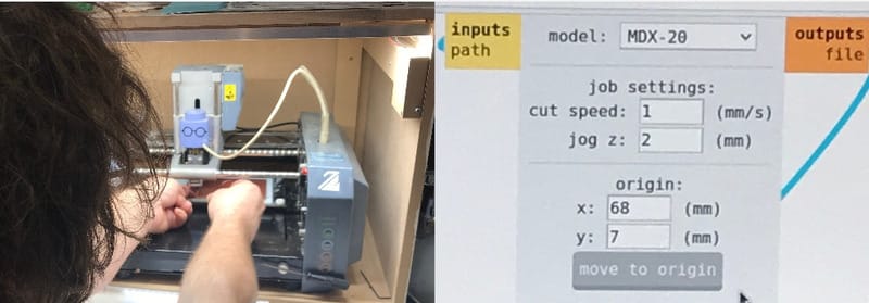
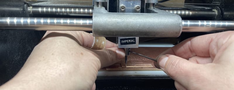
Setting the origin X, Y and Z.
- Lower the millinghead to about 5 mm above the PCB.
- On MODS in the 'RolandMDX /iModela' module push the
move to originbutton. - Look in the machine and estimate how far the origin needs to move.
- Adjust the X an Y values in MODS and push 'move to origin'
- Repeat step 3 and 4 if needed.
- When the right origin is found make a picture of it, because MODS does not remember it.
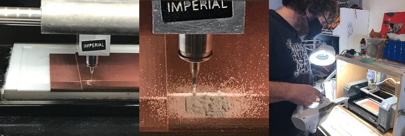
If the millingbit is at the right spot it needs to be lowered on the board.
- Grab the millingbit between 2 fingers.
- Loosen the blue marked screw with the alan key.
- Gently lower the bit onto the board.
- Tap the board slightly so the bit is toughing.
- Fasten the screw (snug).
Ready to mill
- In MODS push
calculate(module mill raster 2D) once more. (step 6 in the first image) - Wait for the file to be ready to sent in the 'Websocket Serial' module and push
send file - take a break! The milling will take quite some time.
 if it is finished, clean up the dust and start the second run with cutting the outline.
Cutting the outline
After the trace-milling is done load the matching image for the outline into mods. The steps for this are almost the same as above.
- Let MODS read the SVG or PNG, now use the matching 'interior.PNG'. Check if the 'artwork' has a DPI between 500 and 1000.
- In the block
setPCB defaults(mm)click the buttonmill outline (1/32)this changes the settings in theMill raster 2Dblock to the default settings for milling the outline. - Some of the settings need to be checked/adjusted in the
Mill raster 2Dblock:- The tooldiameter is 0.8
- Set the cut depth to 0.6 mm.
- Measure the thickness of the board. in our case 1.55 mm. Then set the max depth to 1.6 mm. The rest of the settings are okay.
- Now push
calculate. The 2D milling lines will appear in the small viewer in the module.
- Check the 3D view in the module 'View toolpath' at nr 4. Now it is visible that the mill will get through in 3 turns.
- In the module Roland MDX /iModela the cut speed is set at 4mm/s. The bigger bit is more sturdy so can go faster.
Machine setup
Switching the millingbit
The millingbit for the outline is more sturdy and stuck on the machine with a magnet. When taking the small bit out, be very careful and put it straight back into the bit-box. (picture 1)
Move to the origin.
- Lower the millinghead to about 5 mm above the PCB.
- On MODS in the 'RolandMDX /iModela' module push the
move to originbutton. - Check if the origin is right. (remember, you have a picture of the origin settings)
If the millingbit is at the right spot it needs to be lowered on the board.
- Grab the millingbit between 2 fingers.
- Loosen the blue marked screw with the alan key.
- Gently lower the bit onto the board.
- Tap the board slightly so the bit is toughing.
- Fasten the screw (snug).
Ready to mill
- In MODS push
calculate(module mill raster 2D) once more. (step 6 in the first image) - Wait for the file to be ready to sent in the 'Websocket Serial' module and push
send file - no time for a break, this time the machine will be fast! (picture 2)
If it is finished, clean up the dust Check if the board is loose with the small screwdriver and if so: pop up the board and look at the result. (picture 3)
Working on the board, getting ready to solder.
- If necessary sand of the rough rims with handtowel-paper.
- Look at the board if everything is okay.
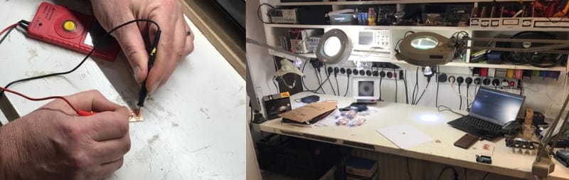
- Check the board with a multimeter if all the connections are okay and if there are no shorts.
- Wash the board with handsoap, to clean of all the grease. Don't touch the top anymore. Now move over to the soldering station:
- Glue the board to a piece of paper, with doublesided tape that way you can move it around with the paper and hold it in place with your hand on the paper.
Soldering
First some basic tips for soldering: 'Be Zen', 'Be one with the soldering', 'Don't drink any coffee and get yourself a good matrass.' 'Use flux!' 'It is like a dance': 1. 2. 3. 4.
- Heat up the board and component-leg.
- Put solder in place
- Take solder away
- Take iron away. and next: 1. 2. 3. 4.
Now the real thing:
- Get the scheme and the picture of the finished product ready and make a plan what to solder first and what later:
- start in the middle and work towards the outside.
- start with the small, lower components and do the higher ones later.
- Pick the first few components (4 or 5 max). Take only one drawer at the time, take out the component, lay it on the paper and put the drawer back in the closet. that way the right components stay in the right drawer. Check if the components have an orientation.
- Get the right soldering ready
- Turn on the iron, wait a minute until the green light starts blinking.
- Turn on the ventilator.
- Clean the Soldering-tip in the brass-sponge and melt a littlebit of solder on the tip. clean again in the sponge.
- Get the first component ready and:
- put a littlebit of solder on the board on one of the connections.
- hold the component with the tweezers and reheat the bit of solder. Place that side of the component on the spot and hold the component in the right direction.
- now start with the connection all the way at the other side of the component and do the solder dance.
- Heat up the board and component-leg.
- Put solder in place
- Take solder away
- Take iron away.
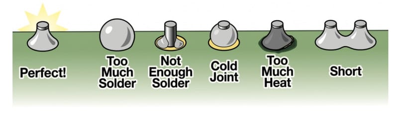
- repeat for all the connections and as last the very first connection.
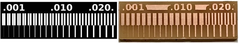
Group assignment
For the group assignment we had a all girls group this time, with Nicole, Paula, Loes an me.
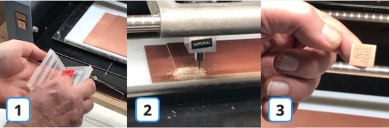
 We worked our way through the masterplan that I wrote above. and made the test-PNG that is shared on the Fab-academy site. It took us quite a long time, but because we all worked together we could figure out all the right settings. We checked the path and everything looked fine, You could already see that the milling-bit was too big for most of the inserts.
 Loes made a picture of the 'origin' and start printing.
My very important task was to change the millingbits. In order to do so, fist move the millinghead to the left-front (by pushing view). Then unscrew the millingbit with the alan-key thats on the front of the machine, while holding it. The 0.8 milling bit can be stuck on the magnet on the front of the machine.
 After that move to the origin and lower the bit carefully onto the board. Tap the board slightly to be sure the millingbit is touching the board.
 We used a 0.4mm-1-flute millingbit, that was brand new, so out project came out fine. With this 0.4mm bit it was possible to make a line in between the copper of 0.16 inches, which equals 0.4064 millimeters. So the bit did exactly what we wanted it to do.
Individual assignments
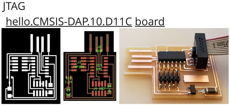
JTAG
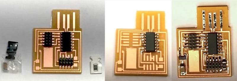
My first project was making a SAM-D prosessor JTAG-programmer. The Hello world board thats in the list, With a SAM-D processor.
milling the board
On thursday we worked all morning an part of the afternoon on the explanation and group assignment, so it was unclear if we would have time to finish printed boards for all 4 of us. For several reasons Loes and I ended up being last. But we teamed up and milled our boards together, thus saving time in getting the right settings. This time I was working the computer and Loes did the changing of the millingbits.
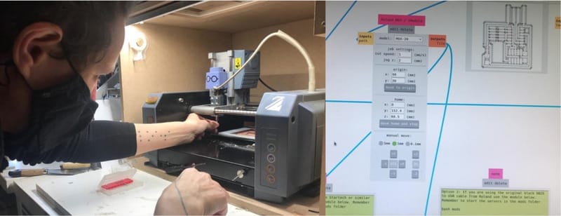 We forgot to remeasure the height when we moved to the second board and therefor it did nog mill deep enough. because we were on a tight schedule we quickly asked Henk for help and he explained the stop and reset procedure.
 After that we did measure the z-origin and everything worked fine.
We ended up keeping Henk longer in Amsterdam, but we both had a milled board at 18.30 that evening.
After that we did measure the z-origin and everything worked fine.
We ended up keeping Henk longer in Amsterdam, but we both had a milled board at 18.30 that evening.
relaxed weekend
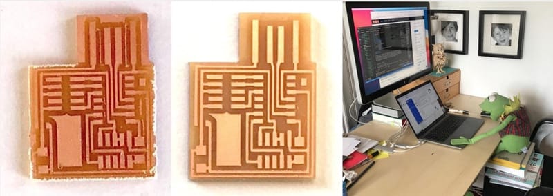
In the weekend there was not much I could do, I proudly showed my 2 bij 3 cm result of 8 hours work on thursday to everyone and I cleaned of the parts that were not needed. I found some time to work on getting a better HUGO-theme. (that will support raw HTML). It was so relaxed that my workspace was taken over...
soldering the board
Monday-afternoon was my lab-time. Soldering! I had my relaxed weekend, tested my matrass, drank no coffee beforehand and felt extremely Zen. So I was up for it.
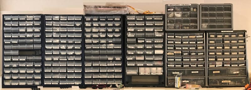
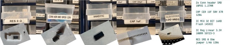
In the morning at home I looked up all the different components and quite a bit of electronics-classes from Highschool came back to me.
But all the names listed on the images where not the same in the componentcloset at Waag. I had no clue where to look for everything and it is right above the workspace. So with the 1,5 meter Covid-regulations it is almost impossible to do a relaxed search.
 Luckily for me,
Loes was already busy all morning and gave me some great images of all the parts that I needed. and an image of the drawers they came out of. So that way I could do it quickly and saved me a lot of time.
Luckily for me,
Loes was already busy all morning and gave me some great images of all the parts that I needed. and an image of the drawers they came out of. So that way I could do it quickly and saved me a lot of time.
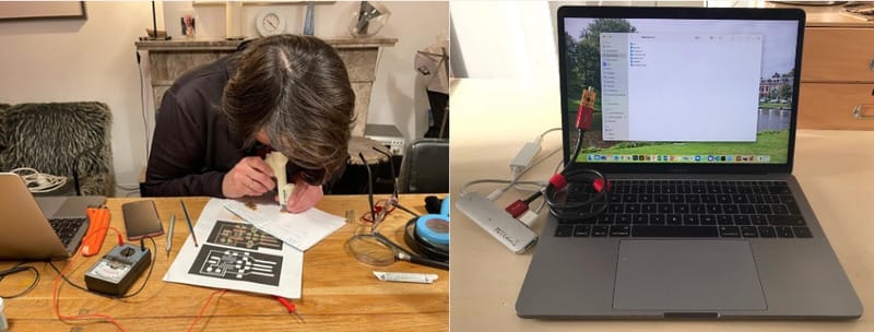
I practices the soldering on a broken board that was left, so I could get the hang of it and especially the amount of solder to add. Since I have some experience soldering bigger electronics at home it was just getting the hang of the size. So with a good amount of 'Zen' I did get it all on-board.
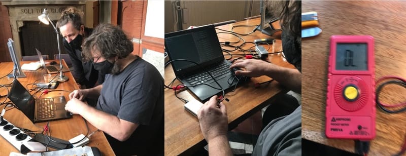
So now the testing with Henk. Loes was also still trying and when the setup was right Henk would try my board as well. Now Henk did test nr 1
 bummer
But I had a plan: measure all the connections with the multimeter. and I found that one leg of the microchip was not connected to the board. So resolder and test with henk nr 2
 grmmmpf
So we had a good talk about what could go wrong, with Henk, Nadieh (who's JTAG miraculously was working and Loes). I did ask earlier that day if the components have a direction (I knew that the capacitors and the resistor wouldn't have one) but I was told by my colleague-students that the microboard was indifferent as well.... NOT. So did Henk tell us. So then we all looked at the boards and Nadiehs and Loeses were fine and mine was the wrong way around. Quite impossible to see, since the letters were not printed on clearly and there was no sign anywhere on the microchip. So I was sent to the airheater and got my microchip loose. I turned it the right way, soldered it carefully, measured the connections et voila... test nr 3:
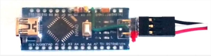
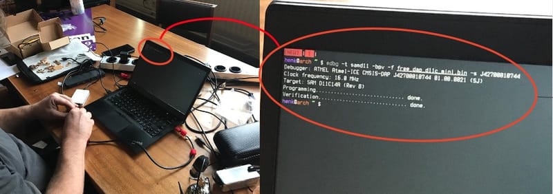 To commemorate this great moment Henk handed me my very own USB-testing-cable with a big smile and I am all set to go on new adventures JTAGging and programming away...
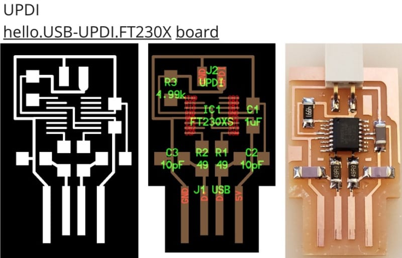
UPDI
Next up, UPDI.
Most of my classmates made this board already, but it is more tricky, the legs of the microprocessor are much closer to each other.
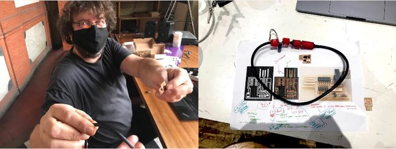
 So while I was waiting for turn-the-chip-around-soldering-time I already took the liberty to mill the next board. Phil picked all the compenents for this board already and could tell me where the difficult ones were. Most components were quite easy, but the 'J2 UPDI' was a two-pin serial-plug had a completely different name on the drawer.
This time I could already pick my components while my board was still milling so I made a A4-paper with double tape on it to get the right stuff layed out clearly.
Henk was leaving early, but Sunke was staying and I had half an hour to solder and clean up the workshop.
So while I was waiting for turn-the-chip-around-soldering-time I already took the liberty to mill the next board. Phil picked all the compenents for this board already and could tell me where the difficult ones were. Most components were quite easy, but the 'J2 UPDI' was a two-pin serial-plug had a completely different name on the drawer.
This time I could already pick my components while my board was still milling so I made a A4-paper with double tape on it to get the right stuff layed out clearly.
Henk was leaving early, but Sunke was staying and I had half an hour to solder and clean up the workshop.
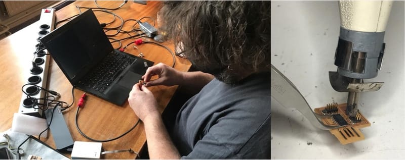
 I took my quick solder home and did the measuring and tidying up of the board at night. I used some eyeglass that I had laying around and my phone as a bright light and it actually worked pretty okay. I changed the phone for a USB-light to have a third hand and I was pretty able to see the small microchip-legs.
 Everybody told me that you could test it by sticking it in you USB. In the evening when I thought and measured it that it seemd fine I stuck it in my computer, but I could not find it in finder...
Time for bed.
On tuesday I cycled towards Amsterdam and there I learned that it is not 'finder' but 'system preferences' where the USB-board shows up.
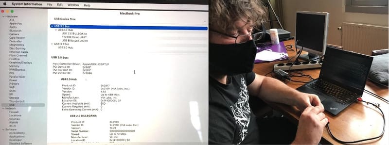 Within 3 minutes I was finished. Henk checked it as wel and was content.
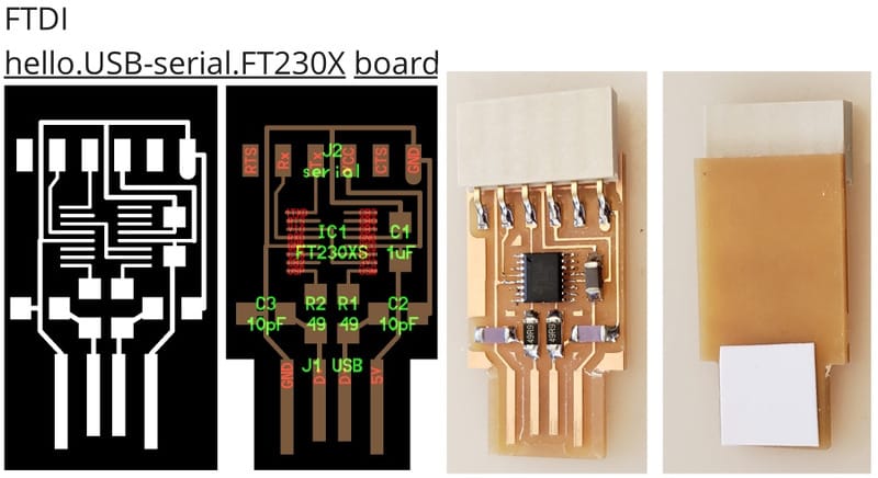
FTDI
With all this spare time in Amsterdam (and I really love the soldering) I decided to make one more thing. Henk said that It would be good to make a FTDI. Easypeacy because it is almost the same as the UPDI, with the same bard, but with a 6-pin FTDI-connector.
First try
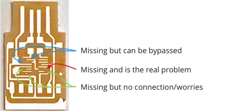
I searched for the right PNG, knew all the settings and switched to the only 2-flute-millingbit that was in the box. but it did not come out right. About half of the small connectors where the microchip should be were not milled right.
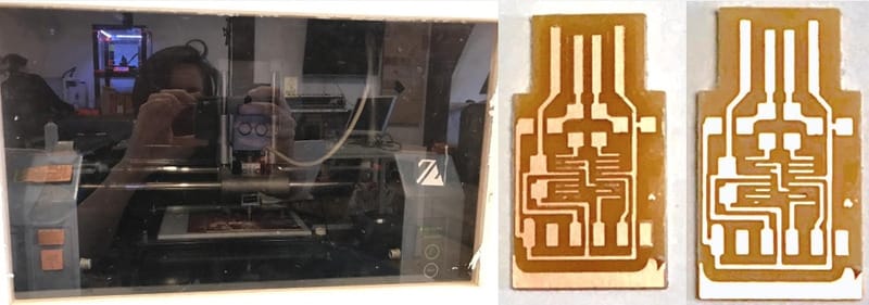 I looked if it were maybe possible to use anyway, but especially the part missing at the red arrow was not possible to fix for me. I showed it to Henk and he suggested to make a new one.
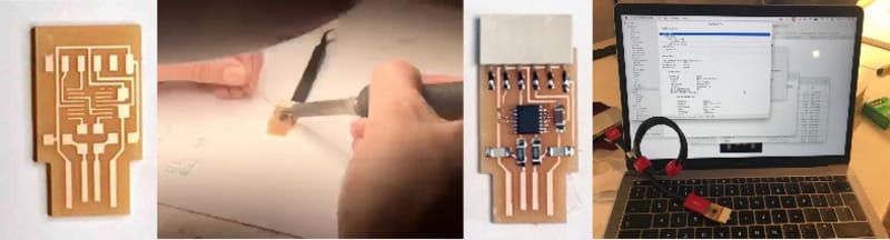
The new one was fine, the soldering went great and the result was directly working.
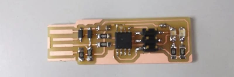
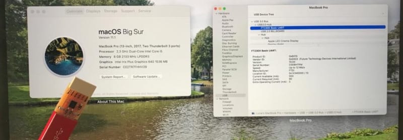
 At home I tested it again and made a better picture.
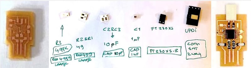
Components and where to find them
While doing this assignment I learned that there is a system in the electronic components. Here is what I know now:
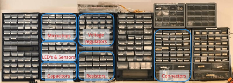 That is about half.... I'm getting there.
Links to Design-files
No design files this week, I only used the standard files that were available on fabacademy